

Datasheet MC145707DW, MC145705DW, MC145705P, MC145706DW, MC145706P Datasheet (Motorola)
...Page 1
MC145705•MC145706•MC145707MOTOROLA
1
Product Preview
#
!! "
#
EIA–232–E and CCITT V.28
The MC145705/06/07 are a series of silicon–gate CMOS transceiver ICs that
fulfill the electrical specifications of EIA–232–E and CCITT V .28 while operating
from a s ingle + 5 V power supply. T hese t ransceiver series a re h igh
performance and low power consumption devices that are equipped with
standby and output enable function.
A voltage doubler and inverter c onvert t he + 5 V to ± 10 V. This i s
accomplished through an on–board 20 kHz oscillator and four inexpensive
external electrolytic capacitors.
The MC145705 is composed of t wo drivers and three r eceivers, t he
MC145706 has three drivers and two receivers, and the MC145707 has three
drivers and three receivers. These drivers and receivers are virtually identical to
those of the MC145407.
Available Driver/Receiver Combinations
Device Drivers Receivers No. of Pins
MC145705 2 3 20
MC145706 3 2 20
MC145707 3 3 24
Drivers:
• ± 7.5 Output Swing
• 300 Ω Power–Off Impedance
• Output Current Limiting
• TTL and CMOS Compatible Inputs
• Three–State Outputs During Standby Mode
• Hold Output OFF (MARK) State by TxEN Pin
Receivers:
• ± 25 V Input Range
• 3 to 7 kΩ Input Impedance
• 0.8 V Hysteresis for Enhanced Noise Immunity
• Three–State Outputs During Standby Mode
Charge Pumps:
• + 5 to ± 10 V Dual Charge Pump Architecture
• Supply Outputs Capable of Driving Three Drivers on the MC145403/06
Simultaneously
• Requires Four Inexpensive Electrolytic Capacitors
• On–Chip 20 kHz Oscillators
This document contains information on a product under development. Motorola reserves the right to change or discontinue this product without notice.
Order this document
by MC145705/D
SEMICONDUCTOR TECHNICAL DATA
P SUFFIX
PLASTIC DIP
CASE 738
ORDERING INFORMATION
MC145705P Plastic DIP
MC145706P Plastic DIP
MC145707P Plastic DIP
MC145705DW SOG Package
MC145706DW SOG Package
MC145707DW SOG Package
P SUFFIX
PLASTIC DIP
CASE 724
DW SUFFIX
SOG PACKAGE
CASE 751E
DW SUFFIX
SOG PACKAGE
CASE 751D
20
1
24
1
20
1
24
1
Motorola, Inc. 1995
REV 1
8/95
Page 2
MC145705•MC145706•MC145707 MOTOROLA
2
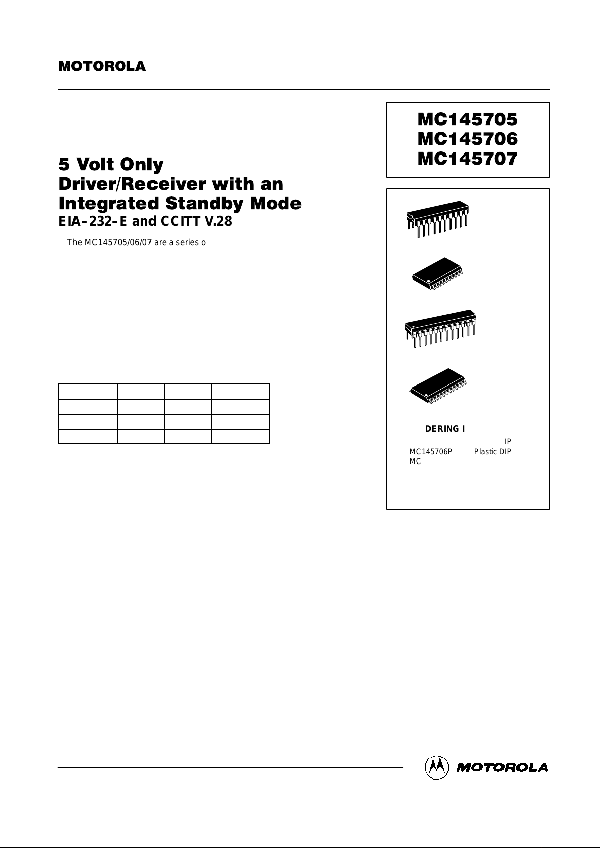
PIN ASSIGNMENTS
MC145706
3 DRIVERS/2 RECEIVERS
MC145705
2 DRIVERS/3 RECEIVERS
MC145707
3 DRIVERS/3 RECEIVERS
C2+
GND
C2–
V
SS
STB
Tx1
Rx1
Tx2
Rx2
Tx3
1
2
3
4
5
6
7
8
9
10
C1+
V
CC
C1–
V
DD
TxEN
DI1
DO1
DI2
DO2
DI3
20
19
18
17
16
15
14
13
12
11
1
2
3
4
5
6
7
8
9
10
20
19
18
17
16
15
14
13
12
11
C1+
V
CC
C1–
V
DD
TxEN
DO1
DO2
DI1
DO3
DI2
C2+
GND
C2–
V
SS
STB
Rx1
Rx2
Tx1
Rx3
Tx2
1
2
3
4
5
6
7
8
9
10
11
12
24
23
22
21
20
19
18
17
16
15
14
13
C2+
GND
C2–
V
SS
STB
NC
Rx1
Tx1
Rx2
Tx2
Rx3
Tx3
C1+
V
CC
C1–
V
DD
TxEN
NC
DO1
DI1
DO2
DI2
DO3
DI3
NC = NO CONNECTION
Page 3
MC145705•MC145706•MC145707MOTOROLA
3
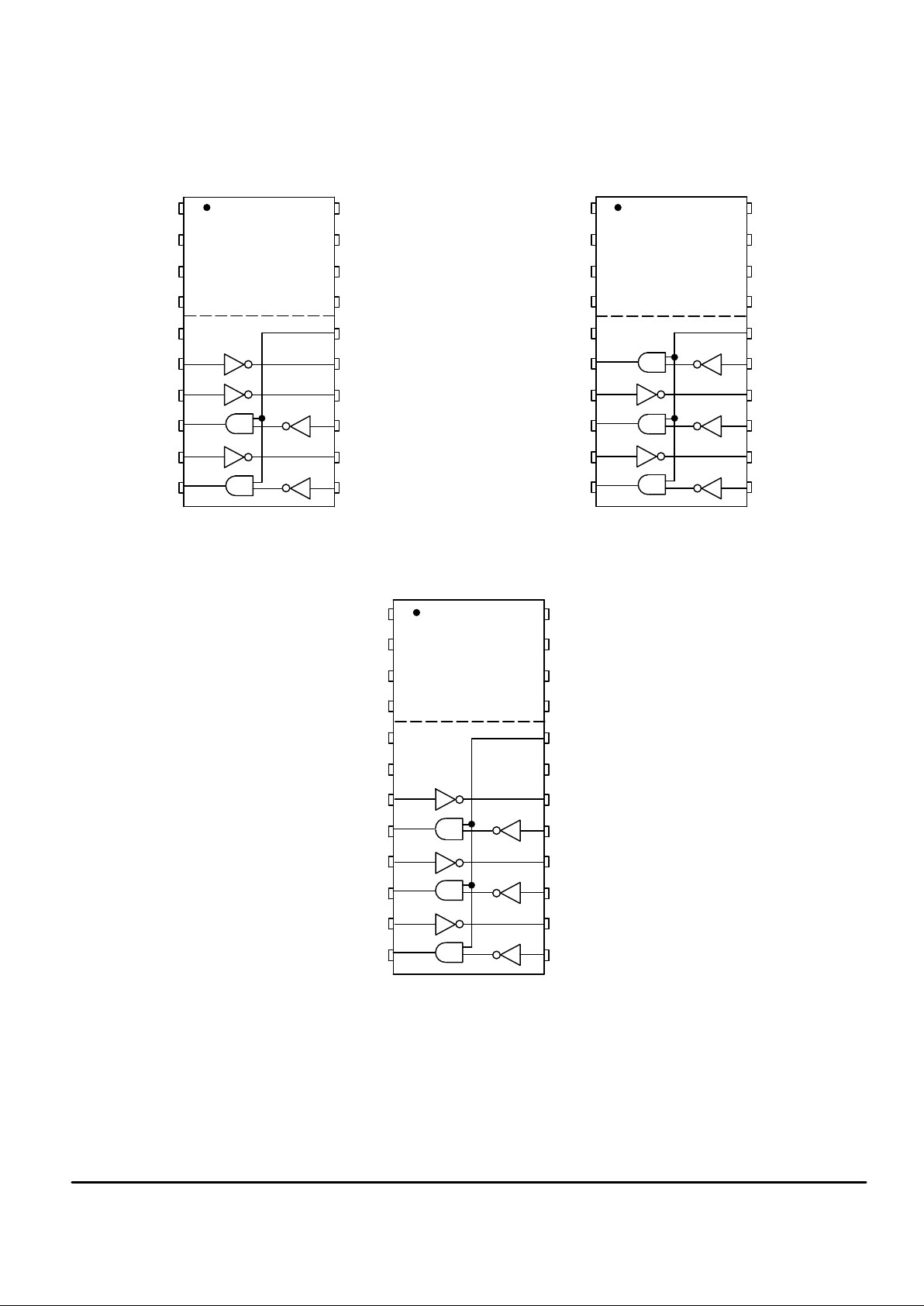
FUNCTION DIAGRAM
RECEIVER
DRIVER
TxEN
CHARGE PUMPS
OSC
VOLTAGE
DOUBLER
VOLTAGE
INVERTER
V
SS
V
DD
V
CC
GND
C1
C3 C4
C2
C1– C1+ C2+ C2–
+
+ +
+
–
+
V
DD
V
DD
V
SS
V
CC
STB
DO
1.0 V
1.8 V
15 k
Ω
5.4 k
Ω
*
*Protection Circuit
LEVEL
SHIFT
STB
V
CC
DI
1.4 V
–
+
V
CC
300
Ω
Tx
V
DD
V
SS
Page 4
MC145705•MC145706•MC145707 MOTOROLA
4
MAXIMUM RATINGS (Voltage Polarities Referenced to GND)
Rating
Symbol Value Unit
DC Supply Voltage V
CC
– 0.5 to + 6.0 V
Input Voltage Rx1 – Rx3 Inputs
DI1 – DI3 Inputs
V
IR
VSS – 15 to VDD+ 15
0.5 to VCC+ 15
V
DC Current per Pin I ± 100 mA
Power Dissipation P
D
1 W
Operating Temperature Range T
A
– 40 to + 85 °C
Storage Temperature Range T
stg
– 85 to + 150 °C
RECOMMENDED OPERATING LIMITS
Parameter Symbol Min Typ Max Unit
Power Supply V
CC
4.5 5 5.5 V
Operating Temperature Range T
A
– 40 — 85 °C
DC ELECTRICAL CHARACTERISTICS (Voltage polarities referenced to GND = 0 V; C1 – C4 = 10 µF; T
A
= – 40 to + 85°C)
Parameter
Symbol Min Typ Max Unit
DC Power Supply V
CC
4.5 5 5.5 V
Quiescent Supply Current (Output Unloaded, Input Low) I
CC
— 1.7 3.5 mA
Quiescent Supply Current (Standby Mode) (Output Unloaded, Input Open) I
CC(STB)
— < 10 20 µA
Control Signal Input Voltage (STB, TxEN) Logic Low
Logic High
V
IL
V
IH
—
VCC – 0.5
—
—
0.5
—
V
Control Signal Input Current Logic Low (TxEN)
Logic High (STB)
I
IL
I
IH
—
—
—
—
– 10
10
µA
Charge Pumps Output Voltage (C1, C2, C3, C4 = 10 µF)
Output Voltage (VDD) I
load
= 0 mA
I
load
= 5 mA
I
load
= 10 mA
V
DD
8.5
7.5
6.0
10.0
9.5
9.0
11
—
—
V
Output Voltage (VSS) I
load
= 0 mA
I
load
= 5 mA
I
load
= 10 mA
V
SS
– 8.5
– 7.5
– 6.0
– 10.0
– 9.2
– 8.6
– 11
—
—
RECEIVER ELECTRICAL SPECIFICATIONS
(Voltage polarities referenced to GND = 0 V; VCC = + 5 V ± 10%; C1 – C4 = 10 µF; TA = – 40 to + 85°C)
Parameter
Symbol Min Typ Max Unit
Input Turn–On Threshold (V
DO1 – DO3
= VOL) Rx1 – Rx3 V
on
1.35 1.8 2.35 V
Input Turn–Off Threshold (V
DO1 – DO3
= VOH) Rx1 – Rx3 V
off
0.75 1 1.25 V
Input Threshold Hysteresis (Von = V
off
) Rx1 – Rx3 V
hys
0.6 0.8 — V
Input Resistance R
in
3 5.4 7 kΩ
High–Level Output Voltage (DO1 – DO3) I
out
= – 20 µA
V
Rx1 – Rx3
= – 3 to – 25 V I
out
= – 1 mA
V
OH
VCC – 0.1
VCC – 0.7
—
4.3
—
—
V
Low–Level Output Voltage (DO1 – DO3) I
out
= + 20 µA
V
Rx1 – Rx3
= + 3 to + 25 V I
out
= + 1.6 mA
V
OL
—
—
0.01
0.5
0.1
0.7
V
This device contains protection circuitry to
guard against damage due to high static
voltages or electric fields. However, precautions must be taken to avoid applications of any
voltage higher than maximum rated voltages to
this high–impedance circuit. For proper operation, it is recommended that the voltage at
the DI and DO pins be constrained to the range
GND ≤ VDI ≤ VDD and GND ≤ VDO ≤ VCC.
Also, the voltage at the Rx pin should be
constrained to (VSS – 15 V) ≤ V
Rx1 – Rx3
≤
(VDD + 15 V), and Tx should be constrained
to VSS ≤ V
Tx1 – Tx3
≤ VDD.
Unused inputs must always be tied to an
appropriate logic voltage level (e.g., GND or
VCC for DI, and GND for Rx).
Page 5

MC145705•MC145706•MC145707MOTOROLA
5
DRIVER ELECTRICAL SPECIFICATIONS
(Voltage polarities referenced to GND = 0 V; VCC = + 5 V ± 10%; C1 – C4 = 10 µF; TA = – 40 to + 85°C)
Parameter
Symbol Min Typ Max Unit
Digital Input Voltage DI1 – DI3
Logic Low
Logic High
V
IL
V
IH
—
2
—
—
0.8
—
V
Input Current DI1 – DI3
VDI = GND
VDI = V
CC
I
IL
I
IH
—
—
7
—
—
± 1.0
µA
Output High Voltage Tx1 – Tx3
(V
DI1 – DI3
= Logic Low, RL = 3 kΩ) Tx1 – Tx6*
V
OH
6
5
7.5
6.5
—
—
V
Output Low Voltage Tx1 – Tx3
(V
DI1 – DI3
= Logic High, RL = 3 kΩ) Tx1 – Tx6*
V
OL
– 6
– 5
– 7.5
– 6.5
—
—
V
Off Source Impedance Tx1 – Tx3 Z
off
300 — — Ω
Output Short Circuit Current (VCC = 5.5 V)
Tx1 – Tx3 Shorted to GND**
Tx1 – Tx3 Shorted to ± 15 V***
I
SC
—
—
—
—
± 60
± 100
mA
*Specifications for a MC14570X powering a MC145406 or MC145403 with three additional drivers/receivers.
**Specification is for one Tx output to be shorted at a time. Should all three driver outputs be shorted simultaneously , device power dissipation
limits could be exceeded.
***This condition could exceed package limitations.
SWITCHING CHARACTERISTICS (V
CC
= + 5 V, ± 10%; C1 – C4 = 10 µF; TA = – 40 to + 85°C)
Parameter
Symbol Min Typ Max Unit
Drivers
Propagation Delay Time Tx1 – Tx3
Low–to–High
(RL = 3 kΩ, CL = 50 pF or 2500 pF)
t
PLH
— 0.5 1
µs
High–to–Low
(RL = 3 kΩ, CL = 50 pF or 2500 pF)
t
PHL
— 0.5 1
Output Slew Rate Tx1 – Tx3
Minimum Load (RL = 7 kΩ, CL = 0 pF)
SR
— ± 6 ± 30
V/µs
Maximum Load (RL = 3 kΩ, CL = 2500 pF) — ± 5 —
Output Disable Time t
DAZ
— 4 10 µs
Output Enable Time t
DZA
— 25 50 ms
Receivers
Propagation Delay Time DO1 – DO3
Low–to–High
t
PLH
— — 1
µs
High–to–Low t
PHL
— — 1
Output Rise Time DO1 – DO3 t
r
— 250 400 ns
Output Fall Time DO1 – DO3 t
f
— 40 100 ns
Output Disable Time t
RAZ
— 4 10 µs
Output Enable Time t
RZA
— 25 50 ms
TRUTH TABLE
Drivers
DI TxEN STB Tx
X X H Z*
X L L L
H H L L
L H L H
*VSS ≤ VTx ≤ V
DD
X = Don’t Care
Receivers
Rx STB DO
X H Z*
H L L
L L H
*GND ≤ VDO ≤ V
CC
X = Don’t Care
Page 6

MC145705•MC145706•MC145707 MOTOROLA
6
PIN DESCRIPTIONS
V
CC
Digital Power Supply
This digital supply pin is connected to the logic power sup-
ply. This pin should have a 0.33 µF capacitor to ground.
GND
Ground
Ground return pin is typically connected t o the signal
ground pin of the EIA–232–D connector (Pin 7) as well as to
the logic power supply ground.
V
DD
Positive Power Supply
This is the positive output of the on–chip voltage doubler
and the positive power supply input of the driver/receiver
sections of the device. This pin requires an external storage
capacitor to filter the 50% duty cycle voltage generated by
the charge pump.
V
SS
Negative Power Supply
This is the negative output of the on–chip voltage doubler/
inverter and the negative power supply input of the driver/
receiver sections of the device. This pin requires an external
storage capacitor to filter the 50% duty cycle voltage generated by the charge pump.
TxEN
Output Enable
This is the driver output enable pin. When this pin is in
logic low level, the condition of the driver outputs (Tx1 – Tx3)
are in keep OFF (mark
) state.
STB
Standby
The device enters the standby mode while this pin is connected to the logic high level. During the standby mode,
driver and receiver output pins become high impedance
state. In this condition, supply current ICC is below 10 µA
(Typ) and can be operated with low current consumption.
C2+, C2–, C1+, C1–
Voltage Doubler and Inverter
These are the connections to the internal voltage doubler
and inverter, which generate the VDD and VSS voltages.
Rx1, Rx2 (Rx3)
Receive Data Input
These are the EIA–232–E receive signal inputs. A voltage
between + 3 and + 25 V is decoded as a space, and causes
the corresponding DO pin to swing to ground (0 V). A voltage
between – 3 and – 25 V is decoded as a mark, and causes
the DO pin to swing up to VCC.
DO1, DO2 (DO3)
Data Output
These are the receiver digital output pins, which swing
from VCC to GND. Each output pin is capable of driving one
LSTTL input load.
Output level of these p ins is high impedance while in
standby mode.
DI1, DI2 (DI3)
Data Input
These are t he high impedance digital input pins to the
drivers. Input voltage levels on these pins must be between
VCC and GND.
The level of these input pins are TTL/CMOS compatible.
Tx1, Tx2 (Tx3)
Transmit Data Output
These are the EIA–232–E transmit signal output pins,
which swing toward VDD and VSS. A logic 1 at a DI input
causes the corresponding Tx output to swing toward VSS.
The actual levels and slew rate achieved will depend on the
output loading (RL/CL).
The minimum output impedance is 300 Ω when turned off.
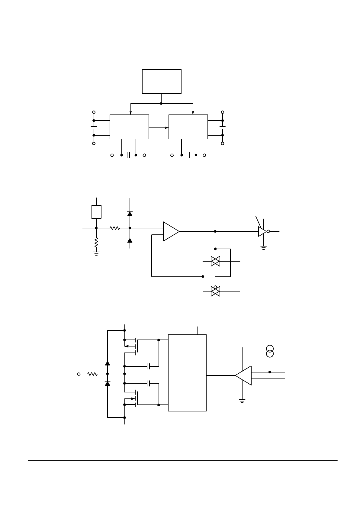
SWITCHING CHARACTERISTICS
RECEIVER
DRIVER
50%
DI1 – DI3
(INPUT)
+ 3 V
0 V
t
f
10%
90%
t
r
t
PHL
t
PLH
V
OL
V
OH
Tx1 – Tx3
(OUTPUT
)
50%
Rx1 – Rx3
(INPUT)
+ 3 V
0 V
t
f
10%
90%
t
r
t
PHL
t
PLH
V
OL
V
OH
DO1 – DO3
(OUTPUT)
STB (INPUT)
Tx1 – Rx3
(OUTPUT)
RECEIVER
DRIVER
+ 5 V
0 V
V
OL
V
OH
+ 1.5 V + 1.5 V
+ 5 V
+ 5 V
– 5 V– 5 V
t
DAZ
t
DZA
STB (INPUT)
DO1 – DO3
(OUTPUT)
+ 5 V
0 V
V
OL
V
OH
+ 1.5 V + 1.5 V
90% 90%
10%10%
t
RAZ
t
RZA
HIGH Z
HIGH Z
Page 7

MC145705•MC145706•MC145707MOTOROLA
7
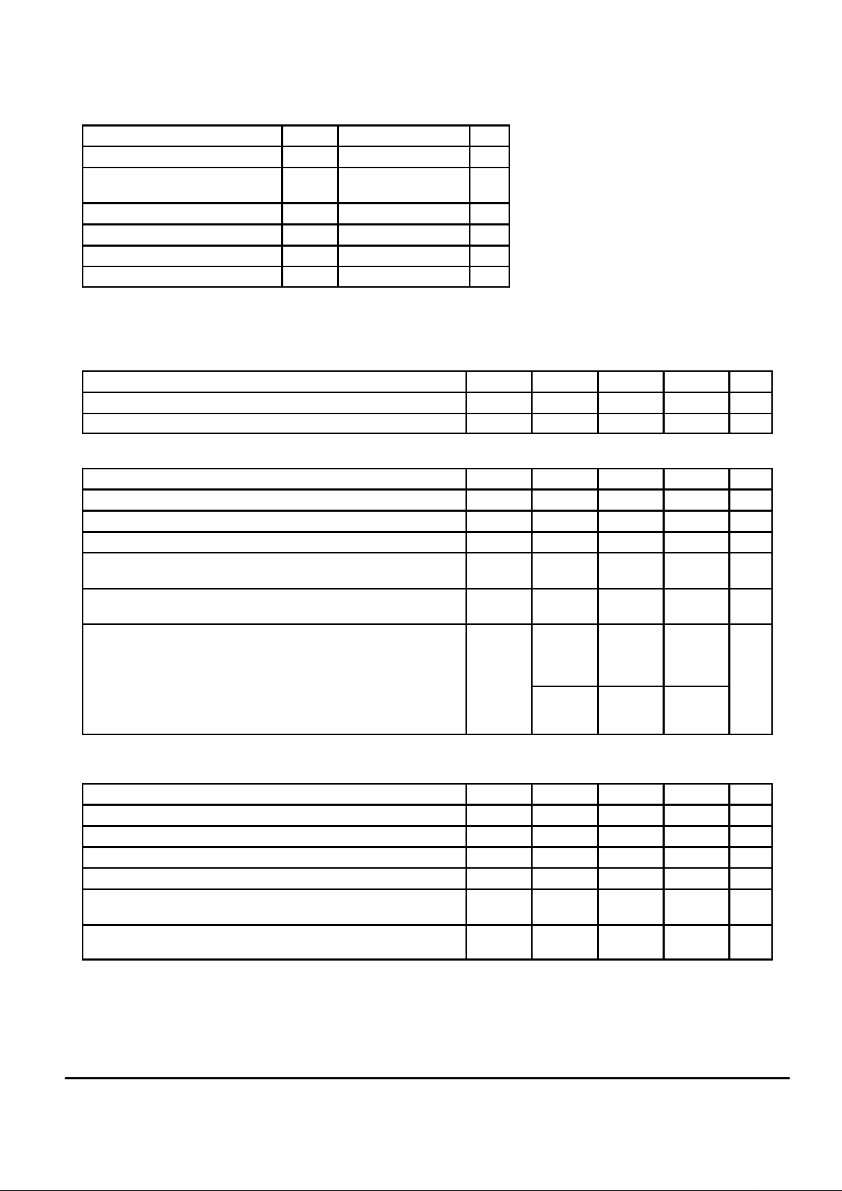
ESD PROTECTION
ESD protection on IC devices that have their pins accessible to the outside world is essential. High static voltages applied to the pins when someone touches them either directly
or indirectly can cause damage to gate oxides and transistor
junctions by coupling a portion of the energy from the I/O pin
to the power supply buses of the IC. This coupling will usually
occur through the internal ESD protection diodes which are
designed to do just that. The key to protecting the IC is to
shunt as much of the energy to ground as possible before it
enters the IC. The figure below shows a technique which will
clamp the ESD voltage at approximately ± 15 V using the
MMBZ15VDLT1. Any residual voltage which appears on the
supply pins is shunted to ground through the capacitors C1
and C2.
1
2
3
4
5
6
7
8
9
10
11
12
24
23
22
21
20
19
18
17
16
15
14
13
C2+
GND
C2–
V
SS
STB
NC
Rx1
Tx1
Rx2
Tx2
Rx3
Tx3
C1+
MMBZ15VDLT1
0.1 µF
C1–
V
DD
TxEN
NC
DO1
DI1
DO2
DI2
DO3
DI3
V
CC
Page 8

MC145705•MC145706•MC145707 MOTOROLA
8
PACKAGE DIMENSIONS
P SUFFIX
PLASTIC DIP
CASE 738–03
1.070
0.260
0.180
0.022
0.070
0.015
0.140
15
°
0.040
1.010
0.240
0.150
0.015
0.050
0.008
0.110
0°
0.020
25.66
6.10
3.81
0.39
1.27
0.21
2.80
0°
0.51
27.17
6.60
4.57
0.55
1.77
0.38
3.55
15
°
1.01
0.050 BSC
0.100 BSC
0.300 BSC
1.27 BSC
2.54 BSC
7.62 BSC
MIN MINMAX MAX
INCHES MILLIMETERS
DIM
A
B
C
D
E
F
G
J
K
L
M
N
NOTES:
1. DIMENSIONING AND TOLERANCING PER ANSI
Y14.5M, 1982.
2. CONTROLLING DIMENSION: INCH.
3. DIMENSION L TO CENTER OF LEAD WHEN
FORMED PARALLEL.
4. DIMENSION B DOES NOT INCLUDE MOLD
FLASH.
-A-
C
K
N
E
G F
D
20 PL
J 20 PL
L
M
-T-
SEATING
PLANE
1 10
1120
0.25 (0.010) T A
M M
0.25 (0.010) T B
M M
B
DW SUFFIX
SOG PACKAGE
CASE 751D–04
NOTES:
1. DIMENSIONING AND TOLERANCING PER
ANSI Y14.5M, 1982.
2. CONTROLLING DIMENSION: MILLIMETER.
3. DIMENSIONS A AND B DO NOT INCLUDE
MOLD PROTRUSION.
4. MAXIMUM MOLD PROTRUSION 0.150
(0.006) PER SIDE.
5. DIMENSION D DOES NOT INCLUDE
DAMBAR PROTRUSION. ALLOWABLE
DAMBAR PROTRUSION SHALL BE 0.13
(0.005) TOTAL IN EXCESS OF D DIMENSION
AT MAXIMUM MATERIAL CONDITION.
–A–
–B–
20
1
11
10
S
A
M
0.010 (0.25) B
S
T
D20X
M
B
M
0.010 (0.25)
P10X
J
F
G
18X
K
C
–T–
SEATING
PLANE
M
R
X 45
_
DIM MIN MAX MIN MAX
INCHESMILLIMETERS
A 12.65 12.95 0.499 0.510
B 7.40 7.60 0.292 0.299
C 2.35 2.65 0.093 0.104
D 0.35 0.49 0.014 0.019
F 0.50 0.90 0.020 0.035
G 1.27 BSC 0.050 BSC
J 0.25 0.32 0.010 0.012
K 0.10 0.25 0.004 0.009
M 0 7 0 7
P 10.05 10.55 0.395 0.415
R 0.25 0.75 0.010 0.029
_ _
_ _
Page 9

MC145705•MC145706•MC145707MOTOROLA
9
P SUFFIX
PLASTIC DIP
CASE 724–03
NOTES:
1. CHAMFERED CONTOUR OPTIONAL.
2. DIMENSION L TO CENTER OF LEADS WHEN
FORMED PARALLEL.
3. DIMENSIONING AND TOLERANCING PER ANSI
Y14.5M, 1982.
4. CONTROLLING DIMENSION: INCH.
–A–
–B–
24 13
12
1
–T–
SEATING
PLANE
24 PL
K
E
F
N
C
D
G
M
A
M
0.25 (0.010) T
24 PLJ
M
B
M
0.25 (0.010) T
L
M
NOTE 1
DIM MIN MAX MIN MAX
MILLIMETERSINCHES
A 1.230 1.265 31.25 32.13
B 0.250 0.270 6.35 6.85
C 0.145 0.175 3.69 4.44
D 0.015 0.020 0.38 0.51
E 0.050 BSC 1.27 BSC
F 0.040 0.060 1.02 1.52
G 0.100 BSC 2.54 BSC
J 0.007 0.012 0.18 0.30
K 0.110 0.140 2.80 3.55
L 0.300 BSC 7.62 BSC
M 0 15 0 15
N 0.020 0.040 0.51 1.01
_ _ _ _
DW SUFFIX
SOG PACKAGE
CASE 751E–04
NOTES:
1. DIMENSIONING AND TOLERANCING PER ANSI
Y14.5M, 1982.
2. CONTROLLING DIMENSION: MILLIMETER.
3. DIMENSIONS A AND B DO NOT INCLUDE
MOLD PROTRUSION.
4. MAXIMUM MOLD PROTRUSION 0.15 (0.006)
PER SIDE.
5. DIMENSION D DOES NOT INCLUDE DAMBAR
PROTRUSION. ALLOWABLE DAMBAR
PROTRUSION SHALL BE 0.13 (0.005) TOTAL IN
EXCESS OF D DIMENSION AT MAXIMUM
MATERIAL CONDITION.
–A–
–B– P12X
D24X
12
1324
1
M
0.010 (0.25) B
M
S
A
M
0.010 (0.25) B
S
T
–T–
G
22X
SEATING
PLANE
K
C
R
X 45
_
M
F
J
DIM MIN MAX MIN MAX
INCHESMILLIMETERS
A 15.25 15.54 0.601 0.612
B 7.40 7.60 0.292 0.299
C 2.35 2.65 0.093 0.104
D 0.35 0.49 0.014 0.019
F 0.41 0.90 0.016 0.035
G 1.27 BSC 0.050 BSC
J 0.23 0.32 0.009 0.013
K 0.13 0.29 0.005 0.011
M 0 8 0 8
P 10.05 10.55 0.395 0.415
R 0.25 0.75 0.010 0.029
____
Page 10

MC145705•MC145706•MC145707 MOTOROLA
10
This page intentionally left blank.
Page 11

MC145705•MC145706•MC145707MOTOROLA
11
This page intentionally left blank.
Page 12

MC145705•MC145706•MC145707 MOTOROLA
12
Motorola reserves the right to make changes without further notice to any products herein. Motorola makes no warranty , representation or guarantee regarding
the suitability of its products for any particular purpose, nor does Motorola assume any liability arising out of the application or use of any product or circuit,
and specifically disclaims any and all liability, including without limitation consequential or incidental damages. “T ypical” parameters can and do vary in different
applications. All operating parameters, including “T ypicals” must be validated for each customer application by customer’s technical experts. Motorola does
not convey any license under its patent rights nor the rights of others. Motorola products are not designed, intended, or authorized for use as components in
systems intended for surgical implant into the body, or other applications intended to support or sustain life, or for any other application in which the failure of
the Motorola product could create a situation where personal injury or death may occur. Should Buyer purchase or use Motorola products for any such
unintended or unauthorized application, Buyer shall indemnify and hold Motorola and its officers, employees, subsidiaries, affiliates, and distributors harmless
against all claims, costs, damages, and expenses, and reasonable attorney fees arising out of, directly or indirectly, any claim of personal injury or death
associated with such unintended or unauthorized use, even if such claim alleges that Motorola was negligent regarding the design or manufacture of the part.
Motorola and are registered trademarks of Motorola, Inc. Motorola, Inc. is an Equal Opportunity/Affirmative Action Employer.
How to reach us:
USA/EUROPE: Motorola Literature Distribution; JAPAN: Nippon Motorola Ltd.; Tatsumi–SPD–JLDC, Toshikatsu Otsuki,
P.O. Box 20912; Phoenix, Arizona 85036. 1–800–441–2447 6F Seibu–Butsuryu–Center, 3–14–2 Tatsumi Koto–Ku, Tokyo 135, Japan. 03–3521–8315
MFAX: RMFAX0@email.sps.mot.com – TOUCHTONE (602) 244–6609 HONG KONG: Motorola Semiconductors H.K. Ltd.; 8B Tai Ping Industrial Park,
INTERNET: http://Design–NET.com 51 Ting Kok Road, Tai Po, N.T., Hong Kong. 852–26629298
MC145705/D
*MC145705/D*
◊
 Loading...