

Page 1
MOTOROLA CMOS LOGIC DATA
1
MC14568B
The MC14568B consists of a phase comparator, a divide–by–4, 16, 64 or
100 counter and a programmable divide–by–N 4–bit binary counter (all
positive–edge triggered) constructed with MOS P–channel and N–channel
enhancement mode devices (complementary MOS) in a monolithic structure.
The MC14568B has been designed for use i n conjunction with a
programmable divide–by–N counter for frequency synthesizers and phase–
locked loop applications requiring low power dissipation and/or high noise
immunity.
This device can be used with both counters cascaded and the output of
the second counter connected to the phase comparator (CTL high), or used
independently of the p rogrammable divide–by–N counter, for example
cascaded with a MC14569B, MC14522B or MC14526B (CTL low).
• Supply Voltage Range = 3.0 to 18 V
• Capable of Driving Two Low–Power TTL Loads, One Low–Power
Schottky TTL Load or Two HTL Loads Over the Rated Temperature
Range.
• Chip Complexity: 549 FETs or 137 Equivalent Gates
MAXIMUM RATINGS* (Voltages referenced to V
SS
)
Rating
Symbol Value Unit
DC Supply Voltage V
DD
– 0.5 to + 18 Vdc
Input Voltage, All Inputs V
in
– 0.5 to VDD + 0.5 Vdc
DC Input Current, per Pin I
in
± 10 mAdc
Power Dissipation, per Package† P
D
500 mW
Operating Temperature Range T
A
– 55 to + 125
_
C
Storage Temperature Range T
stg
– 65 to + 150
_
C
*Maximum Ratings are those values beyond which damage to the device may occur.
†Temperature Derating:
Plastic “P and D/DW” Packages: – 7.0 mW/_C From 65_C To 125_C
Ceramic “L” Packages: – 12 mW/_C From 100_C To 125_C
BLOCK DIAGRAM
PCin14
C1 9
CTL 15
“0” 3
PE 2
D
P3
D
P0
4 5 6 7
VDD = PIN 16
VSS = PIN 8
A
B
PHASE
COMPARATOR
13 PC
out
12 LD
11 G
10 F
1 Q1/C2
TG
TG
TG
COUNTER D1
4–BIT
PROGRAMMABLE
COUNTER D2
PC
in
C1
“0”
P/C
D1
D2
Q1/C2
Q1/C2
PC
out
LD
P/C
D1
D2
C1
“0”
DP2D
P1
(REF.)
CTL HIGH CTL LOW
PC
in
PC
out
LD
SEMICONDUCTOR TECHNICAL DATA
Motorola, Inc. 1995
REV 3
1/94
L SUFFIX
CERAMIC
CASE 620
ORDERING INFORMATION
MC14XXXBCP Plastic
MC14XXXBCL Ceramic
MC14XXXBD SOIC
TA = – 55° to 125°C for all packages.
P SUFFIX
PLASTIC
CASE 648
D SUFFIX
SOIC
CASE 751B
TRUTH TABLE
F G Division Ratio
Pin 10 Pin 11 of Counter D1
0 0 4
0 1 16
1 0 64
1 1 100
The divide by zero state on the programmable divide–by–N 4–bit binary
counter, D2, is illegal.
Page 2
MOTOROLA CMOS LOGIC DATAMC14568B
2
ELECTRICAL CHARACTERISTICS (Voltages Referenced to V
SS
)
V
– 55_C 25_C 125_C
Characteristic
Symbol
V
DD
Vdc
Min Max Min Typ # Max Min Max
Unit
Output Voltage “0” Level
Vin = VDD or 0
V
OL
5.0
10
15
—
—
—
0.05
0.05
0.05
—
—
—
0
0
0
0.05
0.05
0.05
—
—
—
0.05
0.05
0.05
Vdc
“1” Level
Vin = 0 or V
DD
V
OH
5.0
10
15
4.95
9.95
14.95
—
—
—
4.95
9.95
14.95
5.0
10
15
—
—
—
4.95
9.95
14.95
—
—
—
Vdc
Input Voltage#‡ “0” Level
(VO = 4.5 or 0.5 Vdc)
(VO = 9.0 or 1.0 Vdc)
(VO = 13.5 or 1.5 Vdc)
V
IL
5.0
10
15
—
—
—
1.5
3.0
4.0
—
—
—
2.25
4.50
6.75
1.5
3.0
4.0
—
—
—
1.5
3.0
4.0
Vdc
“1” Level
(VO = 0.5 or 4.5 Vdc)
(VO = 1.0 or 9.0 Vdc)
(VO = 1.5 or 13.5 Vdc)
V
IH
5.0
10
15
3.5
7.0
11
—
—
—
3.5
7.0
11
2.75
5.50
8.25
—
—
—
3.5
7.0
11
—
—
—
Vdc
Output Drive Current
(VOH = 2.5 Vdc) Source
(VOH = 4.6 Vdc)
(VOH = 9.5 Vdc)
(VOH = 13.5 Vdc)
I
OH
5.0
5.0
10
15
– 1.2
– 0.25
– 0.62
– 1.8
—
—
—
—
– 1.0
– 0.2
– 0.5
– 1.5
– 1.7
– 0.36
– 0.9
– 3.5
—
—
—
—
– 0.7
– 0.14
– 0.35
– 1.1
—
—
—
—
mAdc
(VOL = 0.4 Vdc) Sink
(VOL = 0.5 Vdc)
(VOL = 1.5 Vdc)
I
OL
5.0
10
15
0.64
1.6
4.2
—
—
—
0.51
1.3
3.4
0.88
2.25
8.8
—
—
—
0.36
0.9
2.4
—
—
—
mAdc
Input Current I
in
15 — ±0.1 — ±0.00001 ±0.1 — ±1.0 µAdc
Input Capacitance C
in
— — — — 5.0 7.5 — — pF
Quiescent Current
(Per Package) Vin = 0 or VDD,
I
out
= 0 µA
I
DD
5.0
10
15
—
—
—
5.0
10
20
—
—
—
0.005
0.010
0.015
5.0
10
20
—
—
—
150
300
600
µAdc
Total Supply Current**†
(Dynamic plus Quiescent,
Per Package)
(CL = 50 pF on all outputs, all
buffers switching)
I
T
5.0
10
15
IT = (0.2 µA/kHz) f + I
DD
IT = (0.4 µA/kHz) f + I
DD
IT = (0.9 µA/kHz) f + I
DD
µAdc
Three–State Leakage Current
Pins 1, 13
I
TL
15 — ±0.1 — ±0.0001 ±0.1 — ±3.0 µAdc
#Noise immunity for worst input combination.
Noise Margin for both “1” and “0” level = 1.0 V min @ VDD = 5.0 V
= 2.0 V min @ VDD = 10 V
= 2.5 V min @ VDD = 15 V
†To calculate total supply current at loads other than 50 pF:
IT(CL) = IT(50 pF) + 1 x 10⁻³ (CL – 50) VDDf
where: IT is in µA (per package), CL in pF, VDD in V, and f in kHz is input frequency.
**The formulas given are for the typical characteristics only at 25_C.
‡Pin 15 is connected to VSS or VDD for input voltage test.
PIN ASSIGNMENT
13
14
15
16
9
10
11
125
4
3
2
1
8
7
6
LD
PC
out
PC
in
CTL
V
DD
C1
F
G
D
P3
“0”
PE
Q1/C2
V
SS
D
P0
D
P1
D
P2
Page 3
MOTOROLA CMOS LOGIC DATA
3
MC14568B
SWITCHING CHARACTERISTICS (C
L
= 50 pF, TA = 25_C)
Characteristic
Symbol
V
DD
V
Min Typ Max Unit
Output Rise Time t
TLH
5.0
10
15
—
—
—
180
90
65
360
180
130
ns
Output Fall Time t
THL
5.0
10
15
—
—
—
100
50
40
200
100
80
ns
Minimum Pulse Width, C1, Q1/C2, or PCin Input t
WH
5.0
10
15
—
—
—
125
60
45
250
120
90
ns
Maximum Clock Rise and Fall Time,
C1, Q1/C2, or PCin Input
t
TLH
,
t
THL
5.0
10
15
15
15
15
—
—
—
—
—
—
µs
PHASE COMPARATOR
Input Resistance R
in
5.0 to 15 — 10
6
— MΩ
Input Sensitivity, dc Coupled — 5.0 to 15 See Input Voltage
Turn–Off Delay Time,
PC
out
and LD Outputs
t
PHL
5.0
10
15
—
—
—
550
195
120
1100
390
240
ns
Turn–On Delay Time.
PC
out
and LD Outputs
t
PLH
5.0
10
15
—
—
—
675
300
190
1350
600
380
ns
DIVIDE–BY–4, 16, 64 OR 100 COUNTER (D1)
Maximum Clock Pulse Frequency
Division Ratio = 4, 64 or 100
f
cl
5.0
10
15
3.0
8.0
10
6.0
16
22
—
—
—
MHz
Division Ratio = 16 5.0
10
15
1.0
3.0
5 0
2.5
6.3
9.7
—
—
—
Propagation Delay Time, Q1/C2 Output
Division Ratio = 4, 64 or 100
t
PLH
,
t
PHL
5.0
10
15
—
—
—
450
190
130
900
380
260
ns
Division Ratio = 16 5.0
10
15
—
—
—
720
300
200
1440
600
400
PROGRAMMABLE DIVIDE–BY–N 4–BIT COUNTER (D2)
Maximum Clock Pulse Frequency
(Figure 3a)
f
cl
5.0
10
15
1.2
3.0
4.0
1.8
8.5
12
—
—
—
MHz
Turn–On Delay Time, “0” Output
(Figure 3a)
t
PLH
5.0
10
15
—
—
—
450
190
130
900
380
260
ns
Turn–Off Delay Time, “0” Output
(Figure 3a)
t
PHL
5.0
10
15
—
—
—
225
85
60
450
170
150
ns
Minimum Preset Enable Pulse Width t
WH(PE)
5.0
10
15
—
—
—
75
40
30
250
100
75
ns
Page 4
MOTOROLA CMOS LOGIC DATAMC14568B
4
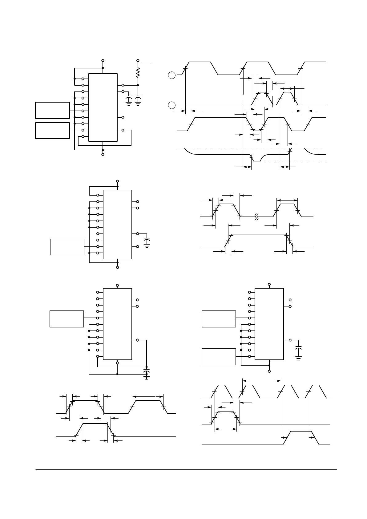
Figure 1. Phase Comparator
DP0PC
out
PULSE
GENERATOR 2
PULSE
GENERATOR 1
“0”
out
REF
PULSE
GENERATOR
PULSE
GENERATOR
PULSE
GENERATOR 1
PULSE
GENERATOR 2
Figure 2. Counter D1
Figure 3. Counter D2
*N is the value programmed on the DP Inputs.
V
DD
V
DD
2
10 k
C
L
C
L
LD
Q1/C2
“0”
V
SS
CTL
D
P1
D
P2
D
P3
PC
in
F
G
C1
PE
A LAGS B, PC
out
IS LOW. A LEADS B, PC
out
IS HIGH.
50%
20 ns
20 ns
t
W(PCin)
90%
50%
10%
t
PLH
t
PLH
t
THL
90%
10%
t
PHL
t
PHL
t
TLH
THREE–STATE THREE–STATE 75%
t
PLH
t
PHL
25%
V
OH
V
OL
PC
in
PG1
LD
PC
out
B
A
V
DD
V
SS
C
L
D
P0
CTL
D
P1
D
P2
D
P3
PC
in
F
G
C1
PE
PC
out
LD
Q1/C2
“0”
20 ns
20 ns
t
W(C1)
t
PHL
10%
50%
90%
t
TLHtTHL
finf
max
90%
50%
10%
C1
Q1/C2
D
P0
D
P1
D
P2
D
P3
PC
in
F
G
C1
PE
CTL
Q1/C2
PC
out
LD
“0”
V
SS
V
DD
a. b.
C
L
D
P0
D
P1
D
P2
D
P3
PC
in
F
G
C1
PE
CTL
Q1/C2
PC
out
LD
“0”
C
L
V
SS
V
DD
t
W(Q1/C2)
20 ns20 ns
90%
50%
10%
90%
50%
10%
Q1/C2
“0”
finf
max
t
PHL
t
PLH
t
TLH
t
THL
N PULSES*
Q1/C2 = PG 1
PE = PG2
20 ns
20 ns
50%
90%
50%
10%
t
W(PE)
“0”
SWITCHING TIME TEST CIRCUITS AND WAVEFORMS
t
PLH
Page 5

MOTOROLA CMOS LOGIC DATA
5
MC14568B
LOGIC DIAGRAM
PC
in
B (REF.)
C1
F
G
“0”
COUNTER
D2
D
Q
C
C
D Q
C
Q
PE
Q
C
D
PC
out
LD
COUNTER
D1
Q1/C2
CTL
PE
14
9
10
11
3
13
1
15
2
VDD = PIN 16
VSS = PIN 8
4 5 6 7
D
P3
D
P2
D
P1
D
P0
A
Page 6

MOTOROLA CMOS LOGIC DATAMC14568B
6
Typical Maximum Frequency Divider D1
Division ratios: 4, 64 or 100 (CL = 50 pF)
Typical Maximum Frequency Divider D1
Division ratio: 16 (CL = 50 pF)
Typical Maximum Frequency Divider D2
Division ratio: 2 (CL = 50 pF)
28
26
24
22
20
18
16
14
12
10
8
6
4
2
0
+100+80+60+ 40+200–20– 40
T, TEMPERATURE (
°
C)
f, FREQUENCY (MHz)
VDD = 15 V
VDD = 10 V
VDD = 5 V
12
10
8
6
4
2
0
+100+80+60+ 40+200–20–40
T, TEMPERATURE (
°
C)
f, FREQUENCY (MHz)
VDD = 15 V
VDD = 10 V
VDD = 5 V
6
5
4
3
2
1
0
+100+80+60+ 40+200–20–40
T, TEMPERATURE (
°
C)
f, FREQUENCY (MHz)
VDD = 15 V
VDD = 10 V
VDD = 5 V
Page 7

MOTOROLA CMOS LOGIC DATA
7
MC14568B
OPERATING CHARACTERISTICS
The MC14568B contains a phase comparator, a fixed
divider (÷ 4, ÷ 16, ÷ 64, ÷ 100) and a programmable divide–
by–N 4–bit counter.
PHASE COMPARATOR
The phase comparator is a positive edge controlled logic
circuit. It essentially consists of four flip–flops and an output
pair of MOS transistors. Only one of its inputs (PCin, pin 14)
is accessible externally. The second is connected to the output of one of the two counters D1 or D2 (see block diagram).
Duty cycles of both input signals (at A and B) need not be
taken into consideration since the comparator responds to
leading edges only.
If both input signals have identical frequencies but different
phases, with signal A (pin 14) leading signal B (Ref.), the
comparator output will be high for the time equal to the
phased difference.
If signal A lags signal B, the output will be low for the same
time. In between, the output will be in a three–state condition
and the voltage on the capacitor of an RC filter normally connected at this point will have some intermediate value (see
Figure 4). When used in a phase locked loop, this value will
adjust the Voltage Controlled Oscillator frequency by reducing the phase difference between the reference signal and
the divided VCO frequency to zero.
Figure 4. Phase Comparator Waveforms
A (PCin)
B (REF.)
PC
out
LD
V
DD
V
SS
V
OH
V
OL
V
OH
V
OL
V
OH
V
OL
1/f
If the input signals have different frequencies, the output
signal will be high when signal B has a lower frequency than
signal A, and low otherwise.
Under the same conditions of frequency difference, the
output will vary between VOH (or VOL) and some intermediate value until the frequencies of both signals are equal and
their phase difference equal to zero, i.e. until locked condition
is obtained.
Capture and lock range will be determined by the VCO frequency range. The comparator is provided with a lock indicator output, which will stay at logic 1 in locked conditions.
The state diagram (Figure 5) depicts the internal state
transitions. It assumes that only one transition on either signal occurs at any time. It shows that a change of the output
state is always associated with a positive transition of either
signal. For a negative transition, the output does not change
state. A p ositive transition may not cause t he output to
change, this happens when the signals have different frequencies.
DIVIDE BY 4, 16, 64 OR 100 COUNTER (D1)
This counter is able to work at an input frequency of 5 MHz
for a VDD value of 10 volts over the standard temperature
range when dividing by 4, 64 and 100. Programming is accomplished by use of inputs F and G (pins 10 and 11) according to the truth table shown. Connecting the Control
input (CTL, pin 15), to VDD allows cascading this counter with
the programmable divide–by–N counter provided in t he
same package. Independent operation is obtained when the
Control input is connected to VSS.
The different division ratios have been chosen to generate
the reference frequencies corresponding to the channel
spacings normally required in frequency synthesizer applications. For example. with the division ratio 100 and a 5 MHz
crystal stabilized source a reference frequency of 50 kHz is
supplied to the comparator. The lower division ratios permit
operation with low frequency crystals.
Figure 5. Phase Comparator State Diagram
00
11
1001
00
11
0110
00
11
1001
INPUT STATE
PC
out
LD
(LOCK DETECT)
0
0
3–STATE
OUTPUT DISCONNECTED
1
1
0
X X
A B
Page 8

MOTOROLA CMOS LOGIC DATAMC14568B
8
If used in cascade with the programmable divide–by–N
counter, practically all usual reference frequencies, or channel spacings of 25, 20, 12.5, 10, 6.25 kHz, etc. are easily
achievable.
PROGRAMMABLE DIVIDE–BY–N
4–BIT COUNTER (D2)
This counter is programmable by using inputs DP0 ... D
P3
(pins 7 ... 4). The Preset Enable input enables the parallel
preset inputs DP0... DP3. The “0” output must be externally
connected to the PE input for single stage applications.
Since there is not a cascade feedback input, this counter,
when cascaded, must be used as the most significant digit.
Because of this, it can be cascaded with binary counters as
well a s with B CD c ounters (MC14569B, MC14522B,
MC14526B).
TYPICAL APPLICATIONS
Figure 6. Cascading MC14568B and MC14522B or MC14526B with MC14569B
f
in
CF
C
MC14569B
ZERO DETECT
CF
C
MC14522B
OR
MC14526B
Q4
PE “0”
CF
C
MC14522B
OR
MC14526B
Q4
PE “0”
Q1/C2
PE “0”
MC14568B
LSD MSD
f
out
DP0 – – – – – – DP3 DP0 – – – – – – DP3 DP0 – – – – – – DP3
Figure 7. Frequency Synthesizer with MC14568B and MC14569B Using a Mixer
(Channel Spacing 10 kHz)
Frequencies shown in parenthesis are given as an example.
(40 kHz)
V
SS
PE
DP0 – – – – DP3
PC
in
C1
CTI
“0”
PC
out
G
F
Q1/C2
V
SS
V
SS
VCO
f
out
(144 – 146 MHz)
V
DD
MC14011
CF
Q
ZERO DETECT
C
CRYSTAL
OSCILLATOR
2 k
2M
MC14568B
MC14569B
MIXER
(143.5 MHz)
Page 9

MOTOROLA CMOS LOGIC DATA
9
MC14568B
Figure 8. Frequency Synthesizer Using MC14568B, MC14569B and MC14522B
(Without Mixer)
Divide ratio = 160N1 + 16N2 + N
3
Example:
f
out
= N1 (MHz) + N2 (x 100 kHz) + N3 (x25 kHz)
Frequency range = 5 MHz
Channel spacing = 25 kHz
Reference frequency = 6.25 kHz
Figures shown in parenthesis refer to example.
Recommended reading:
(1) AN535: “Phase–Lock Techniques”
(2) AR254: “Phase–Locked Loop Design Articles”
(5 MHz)
(VDD)
V
DD
V
DD
PC
in
C1
CTL
“0”
MC14568B
PC
out
G
F
PE
V
SS
V
DD
DP0 – – – – – DP3
VCO
f
out
DP0 – – – – – DP3
C
PE
MC14522B
“0”
Q
ZERO DETECT
(BCD)
BINARY
CF
C
N
1
(0 – 5)
(625 kHz STEPS)
N
2
(0 – 9)
(62.5 kHz STEPS)
N
3
(0, 4, 8, 12)
(6.25 kHz STEPS)
MC14569B
Page 10

MOTOROLA CMOS LOGIC DATAMC14568B
10
TO 455 kHz
IF
REFERENCE
OSCILLATOR
10.24 MHz
X3
÷
2
÷
8
÷
64
÷
N
φ
D
10 kHz
LOOP LOW
PASS FILTER
VCO
16.270–16.560 (17.910) MHz
26.965–27.255
(28.605) MHz
RF
AMP
LOCK DETECTOR
10.695 MHz
RECEIVER
FIRST MIXER
RECEIVER
SECOND MIXER
MC14568B
.91–1.20 (2.55) MHz
N = 91–120 (255) MHz
DOWN
MIXER
÷
N
MC14526B
MIXER
OSCILLATOR
(TRASMIT ONLY)
TO TRANSMITTER
26.965–27.255
(28.605) MHz
10.695 MHz
RCV
TRX
V
DD
NOTE:
1. 10 kHz Channel Spacing
2. Expandable to 165 Channels
(Expanded frequency range
shown in parenthesis)
Figure 9. Typical 23–Channel CB Frequency Synthesizer for
Double Conversion Transceivers
Page 11

MOTOROLA CMOS LOGIC DATA
11
MC14568B
OUTLINE DIMENSIONS
P SUFFIX
PLASTIC DIP PACKAGE
CASE 648–08
ISSUE R
NOTES:
1. DIMENSIONING AND TOLERANCING PER ANSI
Y14.5M, 1982.
2. CONTROLLING DIMENSION: INCH.
3. DIMENSION L TO CENTER OF LEADS WHEN
FORMED PARALLEL.
4. DIMENSION B DOES NOT INCLUDE MOLD FLASH.
5. ROUNDED CORNERS OPTIONAL.
–A–
B
F
C
S
H
G
D
J
L
M
16 PL
SEATING
1 8
916
K
PLANE
–T–
M
A
M
0.25 (0.010) T
DIM MIN MAX MIN MAX
MILLIMETERSINCHES
A 0.740 0.770 18.80 19.55
B 0.250 0.270 6.35 6.85
C 0.145 0.175 3.69 4.44
D 0.015 0.021 0.39 0.53
F 0.040 0.70 1.02 1.77
G 0.100 BSC 2.54 BSC
H 0.050 BSC 1.27 BSC
J 0.008 0.015 0.21 0.38
K 0.110 0.130 2.80 3.30
L 0.295 0.305 7.50 7.74
M 0 10 0 10
S 0.020 0.040 0.51 1.01
____
L SUFFIX
CERAMIC DIP PACKAGE
CASE 620–10
ISSUE V
NOTES:
1. DIMENSIONING AND TOLERANCING PER
ANSI Y14.5M, 1982.
2. CONTROLLING DIMENSION: INCH.
3. DIMENSION L TO CENTER OF LEAD WHEN
FORMED PARALLEL.
4. DIMENSION F MAY NARROW TO 0.76 (0.030)
WHERE THE LEAD ENTERS THE CERAMIC
BODY.
–A–
–B–
–T–
F
E
G
N
K
C
SEATING
PLANE
16 PLD
S
A
M
0.25 (0.010) T
16 PLJ
S
B
M
0.25 (0.010) T
M
L
DIM MIN MAX MIN MAX
MILLIMETERSINCHES
A 0.750 0.785 19.05 19.93
B 0.240 0.295 6.10 7.49
C ––– 0.200 ––– 5.08
D 0.015 0.020 0.39 0.50
E 0.050 BSC 1.27 BSC
F 0.055 0.065 1.40 1.65
G 0.100 BSC 2.54 BSC
H 0.008 0.015 0.21 0.38
K 0.125 0.170 3.18 4.31
L 0.300 BSC 7.62 BSC
M 0 15 0 15
N 0.020 0.040 0.51 1.01
_ _ _ _
16 9
1 8
Page 12

MOTOROLA CMOS LOGIC DATAMC14568B
12
OUTLINE DIMENSIONS
D SUFFIX
PLASTIC SOIC PACKAGE
CASE 751B–05
ISSUE J
NOTES:
1. DIMENSIONING AND TOLERANCING PER ANSI
Y14.5M, 1982.
2. CONTROLLING DIMENSION: MILLIMETER.
3. DIMENSIONS A AND B DO NOT INCLUDE
MOLD PROTRUSION.
4. MAXIMUM MOLD PROTRUSION 0.15 (0.006)
PER SIDE.
5. DIMENSION D DOES NOT INCLUDE DAMBAR
PROTRUSION. ALLOWABLE DAMBAR
PROTRUSION SHALL BE 0.127 (0.005) TOTAL
IN EXCESS OF THE D DIMENSION AT
MAXIMUM MATERIAL CONDITION.
1 8
16 9
SEATING
PLANE
F
J
M
R
X 45
_
G
8 PLP
–B–
–A–
M
0.25 (0.010) B
S
–T–
D
K
C
16 PL
S
B
M
0.25 (0.010) A
S
T
DIM MIN MAX MIN MAX
INCHESMILLIMETERS
A 9.80 10.00 0.386 0.393
B 3.80 4.00 0.150 0.157
C 1.35 1.75 0.054 0.068
D 0.35 0.49 0.014 0.019
F 0.40 1.25 0.016 0.049
G 1.27 BSC 0.050 BSC
J 0.19 0.25 0.008 0.009
K 0.10 0.25 0.004 0.009
M 0 7 0 7
P 5.80 6.20 0.229 0.244
R 0.25 0.50 0.010 0.019
_ _ _ _
How to reach us:
USA/EUROPE/Locations Not Listed: Motorola Literature Distribution; JAPAN: Nippon Motorola Ltd.; Tatsumi–SPD–JLDC, 6F Seibu–Butsuryu–Center,
P.O. Box 20912; Phoenix, Arizona 85036. 1–800–441–2447 or 602–303–5454 3–14–2 Tatsumi Koto–Ku, Tokyo 135, Japan. 03–81–3521–8315
MFAX: RMFAX0@email.sps.mot.com – TOUCHTONE 602–244–6609 ASIA/PACIFIC: Motorola Semiconductors H.K. Ltd.; 8B Tai Ping Industrial Park,
INTERNET: http://Design–NET.com 51 Ting Kok Road, Tai Po, N.T., Hong Kong. 852–26629298
Motorola reserves the right to make changes without further notice to any products herein. Motorola makes no warranty , representation or guarantee regarding
the suitability of its products for any particular purpose, nor does Motorola assume any liability arising out of the application or use of any product or circuit,
and specifically disclaims any and all liability, including without limitation consequential or incidental damages. “Typical” parameters which may be provided
in Motorola data sheets and/or specifications can and do vary in different applications and actual performance may vary over time. All operating parameters,
including “Typicals” must be validated for each customer application by customer’s technical experts. Motorola does not convey any license under its patent
rights nor the rights of others. Motorola products are not designed, intended, or authorized for use as components in systems intended for surgical implant
into the body, or other applications intended to support or sustain life, or for any other application in which the failure of the Motorola product could create a
situation where personal injury or death may occur. Should Buyer purchase or use Motorola products for any such unintended or unauthorized application,
Buyer shall indemnify and hold Motorola and its officers, employees, subsidiaries, affiliates, and distributors harmless against all claims, costs, damages, and
expenses, and reasonable attorney fees arising out of, directly or indirectly, any claim of personal injury or death associated with such unintended or
unauthorized use, even if such claim alleges that Motorola was negligent regarding the design or manufacture of the part. Motorola and are registered
trademarks of Motorola, Inc. Motorola, Inc. is an Equal Opportunity/Affirmative Action Employer .
MC14568B/D
*MC14568B/D*
◊
 Loading...