

Page 1
MOTOROLA CMOS LOGIC DATA
1
MC14560B
The MC14560B adds two 4–bit numbers in NBCD (natural binary coded
decimal) format, resulting in sum and carry outputs in NBCD code.
This device can also subtract when one set of inputs is complemented with
a 9’s Complementer (MC14561B).
All i nputs a nd outputs a re active high. T he carry input for the l east
significant digit is connected to VSS for no carry in.
• Diode Protection on All Inputs
• Supply Voltage Range = 3.0 Vdc to 18 Vdc
• Capable of Driving Two Low–power TTL Loads or One Low–power
Schottky TTL Load Over the Rated Temperature Range
MAXIMUM RATINGS* (Voltages Referenced to V
SS
)
Symbol
Parameter Value Unit
V
DD
DC Supply Voltage – 0.5 to + 18.0 V
Vin, V
out
Input or Output Voltage (DC or Transient) – 0.5 to VDD + 0.5 V
Iin, I
out
Input or Output Current (DC or Transient),
per Pin
± 10 mA
P
D
Power Dissipation, per Package† 500 mW
T
stg
Storage Temperature – 65 to + 150
_
C
T
L
Lead Temperature (8–Second Soldering) 260
_
C
*Maximum Ratings are those values beyond which damage to the device may occur.
†Temperature Derating:
Plastic “P and D/DW” Packages: – 7.0 mW/_C From 65_C To 125_C
Ceramic “L” Packages: – 12 mW/_C From 100_C To 125_C
TRUTH TABLE*
Input Output
A4 A3 A2 A1 B4 B3 B2 B1 CinC
out
S4 S3 S2 S1
0 0 0 0 0 0 0 0 0 0 0 0 0 0
0 0 0 0 0 0 0 0 1 0 0 0 0 1
0 1 0 0 0 0 1 1 0 0 0 1 1 1
0 1 0 0 0 0 1 1 1 0 1 0 0 0
0 1 1 1 0 1 0 0 0 1 0 0 0 1
0 1 1 1 0 1 0 0 1 1 0 0 1 0
1 0 0 0 0 1 0 1 0 1 0 0 1 1
0 1 1 0 1 0 0 0 0 1 0 1 0 0
1 0 0 1 1 0 0 1 1 1 1 0 0 1
*Partial truth table to show logic operation for representative input values.
This device contains protection circuitry to guard against damage
due to high static voltages or electric fields. However, precautions must
be taken to avoid applications of any voltage higher than maximum rated
voltages to this high-impedance circuit. For proper operation, Vin and
V
out
should be constrained to the range VSS ≤ (Vin or V
out
) ≤ VDD.
Unused inputs must always be tied to an appropriate logic voltage
level (e.g., either VSS or VDD). Unused outputs must be left open.
SEMICONDUCTOR TECHNICAL DATA
Motorola, Inc. 1995
REV 3
1/94
Motorola, Inc. 1994
REV 0
1/94
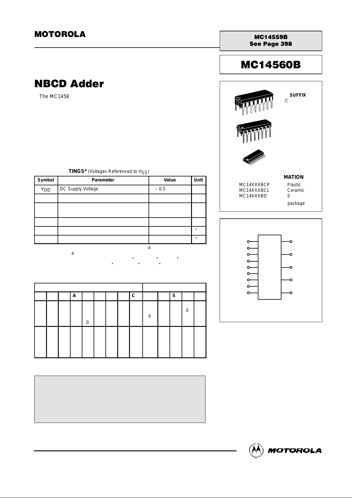
BLOCK DIAGRAM
L SUFFIX
CERAMIC
CASE 620
ORDERING INFORMATION
MC14XXXBCP Plastic
MC14XXXBCL Ceramic
MC14XXXBD SOIC
TA = – 55° to 125°C for all packages.
P SUFFIX
PLASTIC
CASE 648
D SUFFIX
SOIC
CASE 751B
7 13
15
14
1
2
3
4
5
6
12
11
10
9
C
in
A1
B1
A2
B2
A3
B3
A4
B4
S1
S2
S3
S4
C
out
VDD = PIN 16
VSS = PIN 8
Page 2
MOTOROLA CMOS LOGIC DATAMC14560B
2
ELECTRICAL CHARACTERISTICS (Voltages Referenced to V
SS
)
V
– 55_C 25_C 125_C
Characteristic
Symbol
V
DD
Vdc
Min Max Min Typ # Max Min Max
Unit
Output Voltage “0” Level
Vin = VDD or 0
V
OL
5.0
10
15
—
—
—
0.05
0.05
0.05
—
—
—
0
0
0
0.05
0.05
0.05
—
—
—
0.05
0.05
0.05
Vdc
“1” Level
Vin = 0 or V
DD
V
OH
5.0
10
15
4.95
9.95
14.95
—
—
—
4.95
9.95
14.95
5.0
10
15
—
—
—
4.95
9.95
14.95
—
—
—
Vdc
Input Voltage “0” Level
(VO = 4.5 or 0.5 Vdc)
(VO = 9.0 or 1.0 Vdc)
(VO = 13.5 or 1.5 Vdc)
V
IL
5.0
10
15
—
—
—
1.5
3.0
4.0
—
—
—
2.25
4.50
6.75
1.5
3.0
4.0
—
—
—
1.5
3.0
4.0
Vdc
“1” Level
(VO = 0.5 or 4.5 Vdc)
(VO = 1.0 or 9.0 Vdc)
(VO = 1.5 or 13.5 Vdc)
V
IH
5.0
10
15
3.5
7.0
11
—
—
—
3.5
7.0
11
2.75
5.50
8.25
—
—
—
3.5
7.0
11
—
—
—
Vdc
Output Drive Current
(VOH = 2.5 Vdc) Source
(VOH = 4.6 Vdc)
(VOH = 9.5 Vdc)
(VOH = 13.5 Vdc)
I
OH
5.0
5.0
10
15
– 3.0
– 0.64
– 1.6
– 4.2
—
—
—
—
– 2.4
– 0.51
– 1.3
– 3.4
– 4.2
– 0.88
– 2.25
– 8.8
—
—
—
—
– 1.7
– 0.36
– 0.9
– 2.4
—
—
—
—
mAdc
(VOL = 0.4 Vdc) Sink
(VOL = 0.5 Vdc)
(VOL = 1.5 Vdc)
I
OL
5.0
10
15
0.64
1.6
4.2
—
—
—
0.51
1.3
3.4
0.88
2.25
8.8
—
—
—
0.36
0.9
2.4
—
—
—
mAdc
Input Current I
in
15 — ±0.1 — ±0.00001 ±0.1 — ±1.0 µAdc
Input Capacitance
(Vin = 0)
C
in
— — — — 5.0 7.5 — — pF
Quiescent Current
(Per Package)
I
DD
5.0
10
15
—
—
—
5.0
10
20
—
—
—
0.005
0.010
0.015
5.0
10
20
—
—
—
150
300
600
µAdc
Total Supply Current**†
(Dynamic plus Quiescent,
Per Package)
(CL = 50 pF on all outputs, all
buffers switching)
I
T
5.0
10
15
IT = (1.68 µA/kHz) f + I
DD
IT = (3.35 µA/kHz) f + I
DD
IT = (5.03 µA/kHz) f + I
DD
µAdc
#Data labelled “Typ” is not to be used for design purposes but is intended as an indication of the IC’s potential performance.
**The formulas given are for the typical characteristics only at 25_C.
†To calculate total supply current at loads other than 50 pF:
IT(CL) = IT(50 pF) + (CL – 50) Vfk
where: IT is in µA (per package), CL in pF, V = (VDD – VSS) in volts, f in kHz is input frequency, and k = 0.005.
PIN ASSIGNMENT
13
14
15
16
9
10
11
125
4
3
2
1
8
7
6
S2
S1
B1
A1
V
DD
C
out
S4
S3
B3
A3
B2
A2
V
SS
C
in
B4
A4
Page 3
MOTOROLA CMOS LOGIC DATA
3
MC14560B
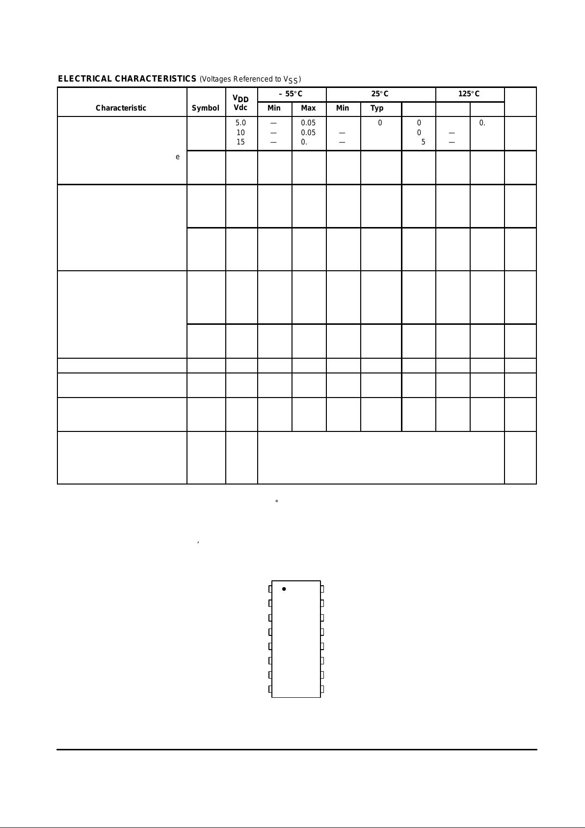
SWITCHING CHARACTERISTICS* (C
L
= 50 pF, TA = 25_C)
Characteristic
Symbol V
DD
Min Typ # Max Unit
Output Rise and Fall Time
t
TLH
, t
THL
= (1.5 ns/pF) CL + 25 ns
t
TLH
, t
THL
= (0.75 ns/pF) CL + 12.5 ns
t
TLH
, t
THL
= (0.55 ns/pF) CL + 9.5 ns
t
TLH
, t
THL
5.0
10
15
—
—
—
100
50
40
200
100
80
ns
Propagation Delay Time
A or B to S
t
PLH
, t
PHL
= (1.7 ns/pF) CL + 665 ns
t
PLH
, t
PHL
= (0.66 ns/pF) CL + 297 ns
t
PLH
, t
PHL
= (0.5 ns/pF) CL + 195 ns
t
PLH
, t
PHL
5.0
10
15
—
—
—
750
330
220
2100
900
675
ns
A or B to C
out
t
PLH
, t
PHL
= (1.7 ns/pF) CL + 565 ns
t
PLH
, t
PHL
= (0.66 ns/pF) CL + 197 ns
t
PLH
, t
PHL
= (0.5 ns/pF) CL + 145 ns
5.0
10
15
—
—
—
650
230
170
1800
600
450
ns
Cin to C
out
t
PLH
, t
PHL
= (1.7 ns/pF) CL + 465 ns
t
PLH
, t
PHL
= (0.66 ns/pF) CL + 187 ns
t
PLH
, t
PHL
= (0.5 ns/pF) CL + 135 ns
5.0
10
15
—
—
—
550
220
160
1500
600
450
ns
Turn–Off Delay Time
Cin to S
t
PLH
= (1.7 ns/pF) CL + 715 ns
t
PLH
= (0.66 ns/pF) CL + 197 ns
t
PLH
= (0.5 ns/pF) CL + 215 ns
t
PLH
5.0
10
15
—
—
—
800
350
240
2250
975
750
ns
Turn–On Delay Time
Cin to S
t
PHL
= (1.7 ns/pF) CL + 565 ns
t
PHL
= (0.66 ns/pF) CL + 197 ns
t
PHL
= (0.5 ns/pF) CL + 145 ns
t
PHL
5.0
10
15
—
—
—
650
230
170
1800
600
450
ns
*The formulas given are for the typical characteristics only at 25_C.
#Data labelled “Typ” is not to be used for design purposes but is intended as an indication of the IC’s potential performance.
Figure 1. Power Dissipation Waveforms
Duty Cycle = 50%
All outputs connected to respective CL loads
f = System clock frequency
Figure 2. Switching Time Waveforms
ALL INPUTS
ANY OUTPUT
20 ns
t
PLH
20 ns
V
DD
V
SS
V
OH
V
OL
90%
50%
10%
2f
1
t
PHL
V
DD
V
SS
V
OH
V
OL
20 ns20 ns
90%
50%
10%
90%
50%
10%
t
TLH
t
THL
ANY INPUT
ANY OUTPUT
Page 4
MOTOROLA CMOS LOGIC DATAMC14560B
4
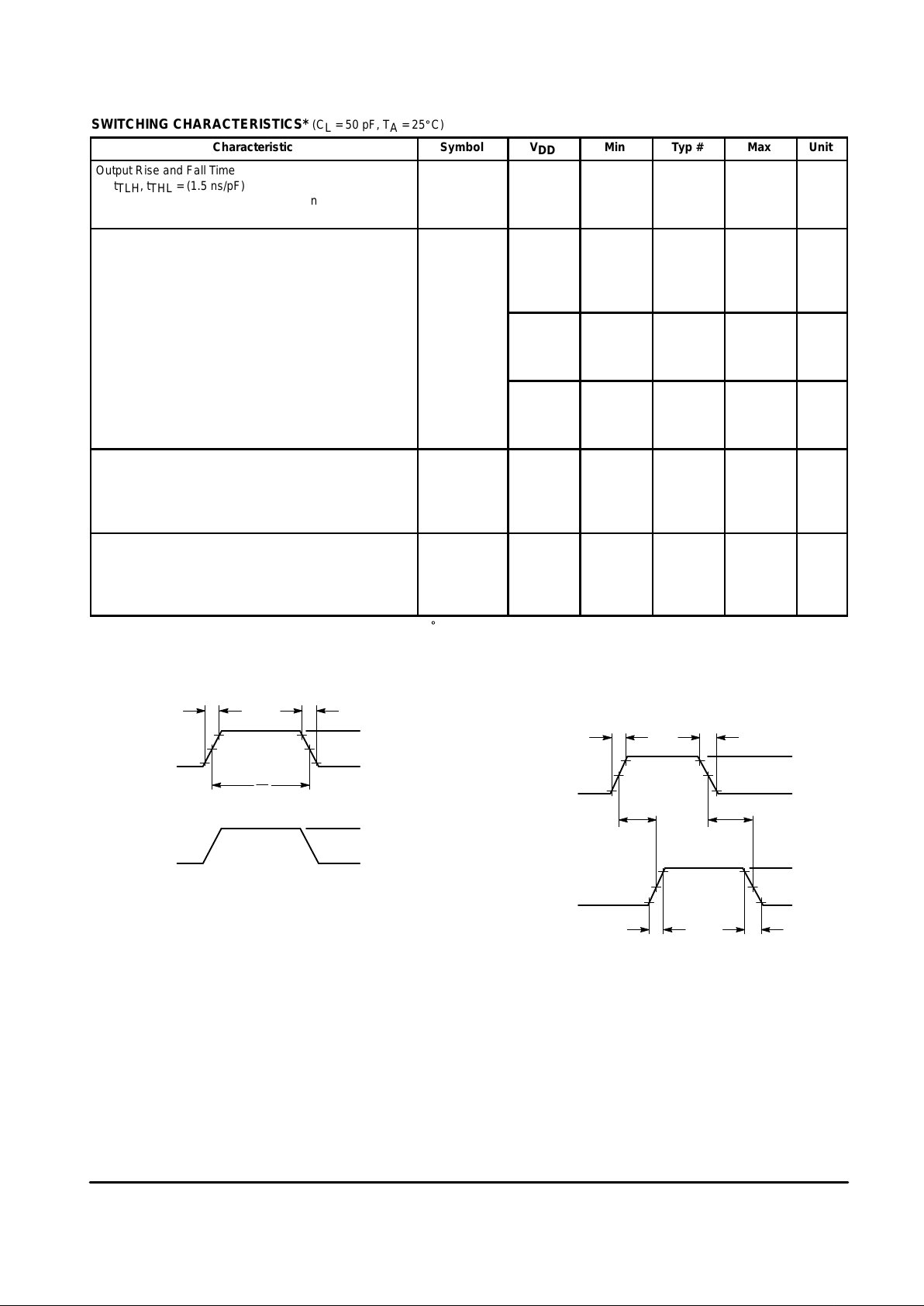
FUNCTIONAL EQUIVALENT LOGIC DIAGRAM
C
in
A1
B1
A2
B2
A3
B3
A4
B4
7
15
14
1
2
3
4
5
6
VDD = PIN 16
VSS = PIN 8
13
C
out
12
11
10
9
S4
S3
S2
S1
Figure 3. Parallel Add/Subtract Circuit
One MC14560B and MC14561B permit a
BCD digit to be added to or subtracted from
a second digit, such as in this typical configuration. A second MC14561B permits either
digit to be added to or subtracted from the
other, or either word to appear unmodified at
the output.
X = Don’t Care
Zero Add/Subtract Result
0 0 B plus A
0 1 B minus A
1 X B
TRUTH TABLE
ADD/SUBTRACT
ZERO
B10
A10
B1
A1
MC14561B
MC14561B
MC14560B
MC14560B
F1
F2
F3
F4
A1
A3
A1A4
COMP
COMP
Z
F1
F2
F3
F4
A2
A3
A4
COMP
COMP
Z
A1
C
in
A2
A2
A3
A4
B1
B2
B3
B4
S3
S2
S1
S4
C
out
UNITS
A1
C
in
A2
A3
A4
B1
B2
B3
B4
S3
S2
S1
S4
C
out
TENS
Page 5

MOTOROLA CMOS LOGIC DATA
5
MC14560B
APPLICATIONS INFORMATION
INTRODUCTION
Frequently in small digital systems, simple decimal arithmetic is performed. Decimal data enters and leaves the system arithmetic unit in a binary coded decimal (BCD) format.
The adder/subtracter in the arithmetic unit may be required
to accept sign as well as magnitude, and generate sign,
magnitude, and overflow. In the past, it has been cumbersome to build sign and magnitude adder/subtracters. Now,
using Motorola’s MSI CMOS functions, the MC14560 NBCD
Adders and MC14561 9’s Complementers, NBCD adder/
subtracters may be built economically, with surprisingly low
package count and moderate speed.
Some background information on BCD arithmetic is presented here, followed by simple circuits for unsigned adder/
subtracters. The final circuit discussed is an adder/subtracter
for signed numbers with complete overflow and sign correction logic.
DECIMAL NUMBER REPRESENTATION
Because logic elements are binary or two–state devices,
decimal digits are generally represented as a group of bits in
a weighted format. There are many possible binary codes
which can be used to represent a decimal number. One of
the most popular codes using 4 binary digits to represent 0
thru 9 is Natural Binary Coded Decimal (NBCD or 8–4–2–1
code).
NBCD is a weighted code. If a value of “0” or “1” is assigned to each of the bit positions, where the rightmost position is 20 and the leftmost is 23, and the values are summed
for a given code, the result is equal to the decimal digit represented by the code. Thus, 01 10 equals 0@23 + 1@22 + 1@21 +
0@20 = 4 + 2 = 6. The 1010, 1011, 1100, 1101, 1110, and 1111
binary codes are not used. Because of these illegal states,
the addition and subtraction of NBCD numbers is more complex than similar calculations on straight binary numbers.
ADDITION OF UNSIGNED NBCD NUMBERS
When 2 NBCD digits, A and B, and a possible carry , C, are
added, a total of 20 digit sums (A + B + C) are possible as
shown in Table 1.
The binary representations for the digit sums 10 thru 19
are offset by 6, the number of unused binary states, and are
not correct. An algorithm for obtaining the correct sum is
shown in Figure 1. A conventional method of implementing
the BCD addition algorithm is shown in Figure 2(a). The
NBCD digits, A and B, are summed by a 4 bit binary full adder. The resultant (sum and carry) is input to a binary/BCD
code converter which generates the correct BCD code and
carry.
An NBCD adder block which performs the above function
is a vailable in a s ingle C MOS p ackage ( MC14560).
Figure 2(b) shows n decades cascaded for addition of n digit
unsigned NBCD numbers. Add time is typically 0.1 + 0.2n µs
for n decades. When the carry out of the most significant decade is a logical “1”, an overflow is indicated.
COMPLEMENT ARITHMETIC
Complement arithmetic is used in NBCD subtraction. That
is, the “complement” of the subtrahend is added to the minuend. The complementing process amounts to biasing the
subtrahend such that all possible sums are positive. Consider the subtraction of the NBCD numbers, A and B:
R = A – B
where R is the result. Now bias both sides of the equation
by 10N – 1 where N is the number of digits in A and B.
R + 10N – 1 A – B + 10N – 1
Rearranging,
R + 10N – 1 A + (10N – 1 – B)
The term (10N – 1 – B), – B biased by 10N – 1, is known as
the 9’s complement of B. When A > B, R + 10N – 1 > 10N – 1;
thus R is a positive number. To obtain R, 1 is added to R +
10N – 1, and the carry term, 10N, is dropped. The addition of
1 is called End Around Carry (EAC).
When A < B, R + 10N – 1 < 10N – 1, no EAC results and R
is a negative number biased by 10N – 1; thus R + 10N – 1 is
the 9’s complement of R.
SUBTRACTION OF UNSIGNED NBCD NUMBERS
Nine’s complement arithmetic requires an element to perform the complementing function. An NBCD 9’s complementer may be implemented using a 4 bit binary adder and 4
inverters, or with combinatorial logic. The Motorola MC14561
9’s complementer is available in a single package. It has true
and inverted complement disable, which allow straight–
through or complement modes of operation. A “zero” line
forces the output to “0”. Figure 3 shows an NBCD subtracter
block using the MC14560 and MC14561. Also shown are n
cascaded blocks for subtraction of n digit unsigned numbers.
Subtract time is 0.6 + 0.4n µs for n stages. Underflow (borrow) is indicated by a logical “0” on the carry output of the
most significant digit. A “0” carry also indicates that the difference is a negative number in 9’s complement form. If the result is input to a 9’s complementer, as shown, and its mode
controlled by the carry out of the most significant digit, the
output of the complementer will be the correct negative magnitude. Note that the carry out of the most significant digit
(MSD) is the input to c arry in of the least significant digit
(LSD). This End Around Carry is required because subtraction is done in 9’s complement arithmetic.
By controlling the complement and overflow logic with an
add/subtract line, both a ddition and subtraction are p erformed using the basic subtracter blocks (Figure 4).
Page 6

MOTOROLA CMOS LOGIC DATAMC14560B
6
Table 1. Sum = A + B + C
Binary Sums
Decimal
Numbers
Corrected
Binary Sums
0000
0001
0010
0011
0100
0101
0110
0111
1000
1001
1010
1011
1100 Non valid
1101 BCD
1110 representation
1111
0000 + Carry
0001 + Carry
0010 + Carry
0011 + Carry
0
1
2
3
4
5
6
7
8
9
10
11
12
13
14
15
16
17
18
19
0000
0001
0010
0011
0100
0101
0110
0111
1000
1001
0000 + Carry
0001 + Carry
0010 + Carry
0011 + Carry
0100 + Carry
0101 + Carry
0110 + Carry
0111 + Carry
1000 + Carry
1001 + Carry
ADDITION AND SUBTRACTION OF SIGNED NBCD
NUMBERS
Using MC14560 NBCD Adders and MC14561 9’s Complementers, a sign and magnitude adder/subtracter can be configured (Figure 5). Inputs A and B are signed positive (AS, B
S
= “0”) or negative (AS, BS = “1”). B is added to or subtracted
from A under control of an Add/Sub line (subtraction = “1”).
The result, R, of the operation is positive signed, positive
signed with overflow, negative signed, or negative signed
with overflow. Add/subtract time is typically 0.6 + 0.4n µs for
n decades.
An exclusive–OR of Add/Sub line and BS produces B′,
which controls the B complementers. If BS, the sign of B, is a
logical “1” (B is negative) and the Add/Sub line is a “0” (add
B to A), then the output of the exclusive–OR (BS′) is a logical
“1” and B is complemented. If BS = “1” and Add/Sub = “1”, B
is not complemented since subtracting a negative number is
the same as adding a positive number. When Add/Sub is a
“1” and BS = “0”, BS′ is a “1” and B is complemented. The A
complementer is controlled by the A sign bit, AS. When AS =
“1”, A is complemented.
Figure 4. Unsigned NBCD Addition Algorithm
6,941
5,870
+
4 BIT BINARY FULL ADDER
DIGIT BINARY SUMS
BINARY SUMS WITH
CARRY FROM CONVERTERS
CODE CONVERTERS
CORRECTED SUM
12,811
A B
C
in
C
out
BINARY TO NBCD
CODE CONVERTER
RESULT, R
A1 B1 A2 B2 A
n
B
n
C
in
C
in
C
in
C
out
C
out
C
out
R1 R2 R
n
OVERFLOW
THOUSANDS
0110
0101
HUNDREDS
1001
1000
TENS
0100
0111
UNITS
0001
0000
ADDER
C
in
ADDER
C
in
ADDER
C
in
ADDER
1 1 0
1011 0001 1011 00011
1100 0010 1011 0001
1
C
out
C
out
C
out
C
out
1 0 0 1 0 1 0 0 0 0 0 0 1 0 0 0 1
Figure 5. Addition of Unsigned NBCD Numbers
(a) MC14560 Block Diagram (b) n–Decade Adder
Typical Add T ime = 0.1 + 0.2n µs
where n = Number of Decades
4 BIT BINARY ADDERS
MC14560 MC14560 MC14560
Page 7

MOTOROLA CMOS LOGIC DATA
7
MC14560B
The truth table and Karnaugh maps for sign, overflow, and
End Around Carry are shown in Figures 6 and 7. Note the
use of BS′ from the exclusive–OR of Add/Sub and BS. BS′
eliminates Add/Sub as a variable in the truth table. As an example of truth table generation, consider an n decade adder/
subtracter where AS = “0”, BS = “1”, and Add/Sub = “0”. B is
in 9’s complement form, 10N – 1 – B. Thus A + (10N – 1 – B)
= 10N – 1 + (A – B). There is no carry when A v B, and the
sign is negative (sign = “1”). When AS and BS are opposite
states and Add/Sub is a “0” (add mode), no overflow can occur (overflow = “0”). The other output states are determined
in a similar manner (see Figure 6).
From the Karnaugh maps it is apparent that End Around
Carry is composed of the two symmetrical functions S2 and
S3 of three variables with AS BS′ C
out
as the center of symmetry. This i s the definition of t he majority l ogic function
M3(ABC). Similarly the Sign is composed of the symmetrical
functions S2(3) and S3(3) but with the center of symmetry
translated to ASBS′ C
out
. This is equivalent to the majority
function M3(ASBS′ C
out
). Further evaluation of the maps and
truth table reveal that Overflow can be generated by the
exclusive–OR function of End Around Carry and Carry Out.
This analysis results in a minimum device count consisting of
one exclusive–OR package and one dual Majority Logic
package to implement BS′, EAC, Sign and Overflow. The
logic connections of these devices are shown in Figure 5.
The output sign, RS, complements the result of the add/
subtract operation when RS = “1”. This is required because
the adder performs 9’s complement arithmetic. Complementing, when RS indicates the result is negative, restores sign
and magnitude convention.
Several variations of the adder/subtracter are possible.
For example, 9’s complement is available at the output of the
NBCD adders, and output complementers are eliminated if
sign and magnitude output is not required.
Figure 6. Subtraction of Unsigned NBCD Numbers
A B
V
DD
Z
C
C
A1 A2 A3 A4
F1 F2 F3 F4
C
n
C
in
A1 A2 A3 A4 B1 B2 B3 AB
C
out
C
n + 1
S1 S2 S3 S4
MC14560
A1 A2 A3 A4
Z
C
C
V
DD
F1 F2 F3 F4
MC14561
FROM C
out
OF MOST SIGNIFICANT
DECADE
RESULT, R
LEAST
SIGNIFICANT
DECADE
A1 B1 A2 B2 A
n
B
n
MOST
SIGNIFICANT
DECADE
C
in
C
C
out
C
in
C
C
out
C
in
C
C
out
R1 R2 R
n
“0” INDICATES
UNDERFLOW
(NEGATIVE RESULT)
(a) Basic Subtracter Block
(b) n–Decade Subtracter
Typical Subtract Time = 0.6 + 0.4n µs where n = Number of Decades
MC14561
BASIC
SUBTRACT
BLOCK
R1
Page 8

MOTOROLA CMOS LOGIC DATAMC14560B
8
SUMMARY
The concepts of binary code representations for decimal
numbers, addition, and complement subtraction were discussed in detail. Using the basic Adder and Complementer
MSI blocks, adder/subtracters for both signed and unsigned
numbers were illustrated with examples.
REFERENCES
1. Chu, Y.:
Digital Computer Design Fundamentals
, New
York, McGraw–Hill, 1962.
2.
McMOS Handbook
, Motorola Inc., 1st Edition.
3. Beuscher, H.:
Electronic Switching Theory and Circuits
,
New York, Van Nostrand Reinhold, 1971.
4. Garrett, L.: CMOS May Help Majority Logic Win Designer’s Vote,
Electronics
, July 19, 1973.
5. Richards, R.:
Digital Design
, New York, Wiley–
Interscience, 1971.
Figure 7. Adder/Subtracter for Unsigned NBCD Numbers
A1 B1 A2 B2 A
n
B
n
C
in
C
C
out
C
in
C
C
out
C
in
C
C
out
R1 R2 R
n
MSD
BASIC
SUBTRACT
BLOCK
LSD
ADD/SUBTRACT
(“1”/“0”)
1/6 MC14572
1/6 MC14572
OVERFLOW = “1”
UNDERFLOW = “1”
(NEGATIVE RESULT)
Typical Add/Subtract Time = 0.6 + 0.4 n µs
where n = Number of Decades
Page 9

MOTOROLA CMOS LOGIC DATA
9
MC14560B
Figure 8. Sign and Magnitude Adder/Subtracter with Overflow
B
n
A
n
B2A2
MC14561MC14561MC14561MC14561
MC14560MC14560
MC14561MC14561
R
n
R2
C
out
C
out
OVERFLOW
SIGN OF R
S
1/4 MC14070
SIGN
Z
Z
W
W
V
DD
EAC
B1A1
MC14561MC14561
M
5
M
5
MC14561
MC14560
C
out
MC14530
A
B
C
D
E
A
B
C
D
E
CCZ
R1
A1 A2 A3 A4
F1 F2 F3 F4
A1 A2 A3 A4 B1 B2 B3 B4
S1 S2 S3 S4
A1 A2 A3 A4
F1 F2 F3 F4
A1 A2 A3 A4
F1 F2 F3 F4
CCZ
C
in
1/4 MC14070
1/4 MC14070
B
S
′
V
DD
A
S
B
S
ADD/SUB
Typical Add/Subtract Time = 0.6 + 0.4n s
where n = Number of Decades
µ
CCZ
Page 10

MOTOROLA CMOS LOGIC DATAMC14560B
10
Inputs
Arithmatic Expression
for R* (Result)
Outputs
(N = Number of Digits,
10N = Modulus
End Around
A
S
“1” = Neg
BS′
“1” = Neg
C
out
“1” = Carry
A, B, R are Positive
Magnitudes)
Carry (EAC)
“1” = EAC
Sign of R
“1” = Negative
Overflow
“1” = Overflow
0 0 0
R = A + 8
No EAC (“0”)
because R is correct
result.
Since A and B are
positive signed, R is
positive signed (“0”).
When C
out
= “0”, there
is no carry (R < 10N)
and thus no overflow
(“0”).
0 0 1
When C
out
= “1”, there
is a carry (R ≥ 10N)
and thus overflow
(“1”).
0 1 0
R = A – B
= A + (10N – 1 – B)
= A – B + 10N – 1
No EAC (“0”)
because 9’s
complement
expression for R is
correct result.
A v B when C
out
=
“0”; thus sign of R
must be negative
(“1”).
0 1 1
EAC = “1” because
expression for R is in
error by 1.
A > B when C
out
=
“1”; thus sign of R
must be positive
(“0”).
There is never an
overflow when
1 0 0
R = B – A
= B + (10N – 1 – A)
= B – A + 10N – 1
No EAC (“0”)
because 9’s
complement
expression for R is
correct result.
B v A when C
out
=
“0”; thus sign of R
must be negative
(“1”).
overflow when
numbers of opposite
sign are added.
1 0 1
EAC = “1” because
expression for R is in
error by 1.
B > A when C
out
=
“1”; thus sign of R
must be positive
(“0”).
1 1 0
R = – A – B
= (10N – 1 – A) +
(10N – 1 – B)
= – (A + B) + 2 x
EAC = “1” because
9’s complement
expression for R is in
error by 1.
Since A and B are
negative signed. R is
negative signed (“1”).
When C
out
= “0”, there
is no Carry (R < 0N)
and (A + B) > 10N – 1
indicating overflow
(“1”).
1 1 1
10N – 2
When C
out
= “1”, there
is a carry (R ≥ 10N)
and (A + B) v 10N – 1
indicating no overflow
(“0”).
*Output of Adders
Figure 9. Truth Table Generation for EAC, Sign, and Overflow Logic
Page 11

MOTOROLA CMOS LOGIC DATA
11
MC14560B
TRUTH TABLE
Inputs Outputs
A
S
BS′ C
out
EAC SGN OVF
0 0 0 0 0 0
0 1 0 0 1 0
1 0 0 0 1 0
1 1 0 1 1 1
0 0 1 0 0 1
0 1 1 1 0 0
1 0 1 1 0 0
1 1 1 1 1 0
BS = (Add/Sub) ę B
S
AS = Sign of A (“1” = Negative)
BS = Sign of B (“1” = Negative)
C
out
= Adder Carry Out
Figure 10. Mapping of EAC, Sign and Overflow Logic
0 1
1 1
0 1
0* 0
End Around Carry
A
S
C
out
B
S′
1 1
0 1
0* 0
0 1
Sign (SGN)
A
S
C
out
B
S′
0 1
0 0
1 0
0 0
Overflow (OVF)
A
S
C
out
B
S′
*= Center of Symmetry
EAC = S2 (ASBS′ C
out
) + S3 (ASBS′ C
out
)
= M3 (ASBS′ C
out
)
SGN = S2 (ASBS′ C
out
) + S3 (ASBS′ C
out
)
= M3 (ASBS′ C
out
)
0 1
1 1
0 1
0 0
EAC
0 0
1 1
1 1
0 0
C
out
0 1
0 0
1 0
0 0
OVF
ę
=
ę
=
KARNAUGH MAPS
Page 12

MOTOROLA CMOS LOGIC DATAMC14560B
12
OUTLINE DIMENSIONS
P SUFFIX
PLASTIC DIP PACKAGE
CASE 648–08
ISSUE R
NOTES:
1. DIMENSIONING AND TOLERANCING PER ANSI
Y14.5M, 1982.
2. CONTROLLING DIMENSION: INCH.
3. DIMENSION L TO CENTER OF LEADS WHEN
FORMED PARALLEL.
4. DIMENSION B DOES NOT INCLUDE MOLD FLASH.
5. ROUNDED CORNERS OPTIONAL.
–A–
B
F
C
S
H
G
D
J
L
M
16 PL
SEATING
1 8
916
K
PLANE
–T–
M
A
M
0.25 (0.010) T
DIM MIN MAX MIN MAX
MILLIMETERSINCHES
A 0.740 0.770 18.80 19.55
B 0.250 0.270 6.35 6.85
C 0.145 0.175 3.69 4.44
D 0.015 0.021 0.39 0.53
F 0.040 0.70 1.02 1.77
G 0.100 BSC 2.54 BSC
H 0.050 BSC 1.27 BSC
J 0.008 0.015 0.21 0.38
K 0.110 0.130 2.80 3.30
L 0.295 0.305 7.50 7.74
M 0 10 0 10
S 0.020 0.040 0.51 1.01
____
L SUFFIX
CERAMIC DIP PACKAGE
CASE 620–10
ISSUE V
NOTES:
1. DIMENSIONING AND TOLERANCING PER
ANSI Y14.5M, 1982.
2. CONTROLLING DIMENSION: INCH.
3. DIMENSION L TO CENTER OF LEAD WHEN
FORMED PARALLEL.
4. DIMENSION F MAY NARROW TO 0.76 (0.030)
WHERE THE LEAD ENTERS THE CERAMIC
BODY.
–A–
–B–
–T–
F
E
G
N
K
C
SEATING
PLANE
16 PLD
S
A
M
0.25 (0.010) T
16 PLJ
S
B
M
0.25 (0.010) T
M
L
DIM MIN MAX MIN MAX
MILLIMETERSINCHES
A 0.750 0.785 19.05 19.93
B 0.240 0.295 6.10 7.49
C ––– 0.200 ––– 5.08
D 0.015 0.020 0.39 0.50
E 0.050 BSC 1.27 BSC
F 0.055 0.065 1.40 1.65
G 0.100 BSC 2.54 BSC
H 0.008 0.015 0.21 0.38
K 0.125 0.170 3.18 4.31
L 0.300 BSC 7.62 BSC
M 0 15 0 15
N 0.020 0.040 0.51 1.01
_ _ _ _
16 9
1 8
Page 13

MOTOROLA CMOS LOGIC DATA
13
MC14560B
OUTLINE DIMENSIONS
D SUFFIX
PLASTIC SOIC PACKAGE
CASE 751B–05
ISSUE J
NOTES:
1. DIMENSIONING AND TOLERANCING PER ANSI
Y14.5M, 1982.
2. CONTROLLING DIMENSION: MILLIMETER.
3. DIMENSIONS A AND B DO NOT INCLUDE
MOLD PROTRUSION.
4. MAXIMUM MOLD PROTRUSION 0.15 (0.006)
PER SIDE.
5. DIMENSION D DOES NOT INCLUDE DAMBAR
PROTRUSION. ALLOWABLE DAMBAR
PROTRUSION SHALL BE 0.127 (0.005) TOTAL
IN EXCESS OF THE D DIMENSION AT
MAXIMUM MATERIAL CONDITION.
1 8
16 9
SEATING
PLANE
F
J
M
R
X 45
_
G
8 PLP
–B–
–A–
M
0.25 (0.010) B
S
–T–
D
K
C
16 PL
S
B
M
0.25 (0.010) A
S
T
DIM MIN MAX MIN MAX
INCHESMILLIMETERS
A 9.80 10.00 0.386 0.393
B 3.80 4.00 0.150 0.157
C 1.35 1.75 0.054 0.068
D 0.35 0.49 0.014 0.019
F 0.40 1.25 0.016 0.049
G 1.27 BSC 0.050 BSC
J 0.19 0.25 0.008 0.009
K 0.10 0.25 0.004 0.009
M 0 7 0 7
P 5.80 6.20 0.229 0.244
R 0.25 0.50 0.010 0.019
_ _ _ _
How to reach us:
USA/EUROPE/Locations Not Listed: Motorola Literature Distribution; JAPAN: Nippon Motorola Ltd.; Tatsumi–SPD–JLDC, 6F Seibu–Butsuryu–Center,
P.O. Box 20912; Phoenix, Arizona 85036. 1–800–441–2447 or 602–303–5454 3–14–2 Tatsumi Koto–Ku, Tokyo 135, Japan. 03–81–3521–8315
MFAX: RMFAX0@email.sps.mot.com – TOUCHTONE 602–244–6609 ASIA/PACIFIC: Motorola Semiconductors H.K. Ltd.; 8B Tai Ping Industrial Park,
INTERNET: http://Design–NET.com 51 Ting Kok Road, Tai Po, N.T., Hong Kong. 852–26629298
Motorola reserves the right to make changes without further notice to any products herein. Motorola makes no warranty , representation or guarantee regarding
the suitability of its products for any particular purpose, nor does Motorola assume any liability arising out of the application or use of any product or circuit,
and specifically disclaims any and all liability, including without limitation consequential or incidental damages. “Typical” parameters which may be provided
in Motorola data sheets and/or specifications can and do vary in different applications and actual performance may vary over time. All operating parameters,
including “Typicals” must be validated for each customer application by customer’s technical experts. Motorola does not convey any license under its patent
rights nor the rights of others. Motorola products are not designed, intended, or authorized for use as components in systems intended for surgical implant
into the body, or other applications intended to support or sustain life, or for any other application in which the failure of the Motorola product could create a
situation where personal injury or death may occur. Should Buyer purchase or use Motorola products for any such unintended or unauthorized application,
Buyer shall indemnify and hold Motorola and its officers, employees, subsidiaries, affiliates, and distributors harmless against all claims, costs, damages, and
expenses, and reasonable attorney fees arising out of, directly or indirectly, any claim of personal injury or death associated with such unintended or
unauthorized use, even if such claim alleges that Motorola was negligent regarding the design or manufacture of the part. Motorola and are registered
trademarks of Motorola, Inc. Motorola, Inc. is an Equal Opportunity/Affirmative Action Employer .
MC14560B/D
*MC14560B/D*
◊
 Loading...