

Page 1
The MC1455 monolithic timing circuit is a highly stable controller capable
of producing accurate time delays or oscillation. Additional terminals are
provided for triggering or resetting if desired. In the time delay mode, time is
precisely controlled by one external resistor and capacitor. For astable
operation as an oscillator, the free–running frequency and the duty cycle are
both accurately controlled with two external resistors and one capacitor. The
circuit may be triggered and reset on falling waveforms, and the output
structure can source or sink up to 200 mA or drive MTTL circuits.
• Direct Replacement for NE555 Timers
• Timing from Microseconds through Hours
• Operates in Both Astable and Monostable Modes
• Adjustable Duty Cycle
• High Current Output Can Source or Sink 200 mA
• Output Can Drive MTTL
• Temperature Stability of 0.005% per °C
• Normally ON or Normally OFF Output
Order this document by MC1455/D
TIMING CIRCUIT
SEMICONDUCTOR
TECHNICAL DATA
P1 SUFFIX
PLASTIC PACKAGE
CASE 626
8
1
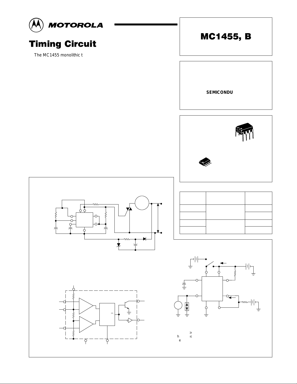
Figure 1. 22 Second Solid State Time Delay Relay Circuit
38
10 k
0.1 µF
0.01
t = 1.1; R and C = 22 sec
Time delay (t) is variable by
changing R and C (see Figure 16).
4
2
MC1455
5
µ
F
1.0 k
6
R
7
µ
F
1.0
1
1N4740
20 M
C
MT2
G
–10 V
3.5 k
MT1
250 V–+
Load
1N4003
10 µF
Figure 2. Representative Block Diagram
V
CC
8
Threshold
Control Voltage
Trigger
5 k
6
5
2
5 k
5 k
+
Comp
A
–
+
Comp
B
–
Gnd Reset
R
S
1
Flip
Flop
Inhibit/
Reset
4
Q
7
3
117 Vac/60 Hz
Discharge
Output
D SUFFIX
8
1
PLASTIC PACKAGE
CASE 751
(SO–8)
ORDERING INFORMATION
Operating
Device
MC1455P1
MC1455D
MC1455BD SO–8
MC1455BP1 Plastic DIP
Temperature Range
TA = 0° to +70°C
TA = – 40° to +85°C
Package
Plastic DIP
SO–8
Figure 3. General T est Circuit
V
I
V
CC
2
CC
7
Discharge
Threshold
6
Trigger
V
R
Reset 4 8
Control
Voltage
Output
I
Sink
I
Source
5
MC1455
3
Gnd
1
+
0.01
µ
F
V
O
Test circuit for measuring DC parameters (to set output and
measure parameters):
a) When VS w 2/3 VCC, VO is low.
b) When VS v1/3 VCC, VO is high.
c) When VO is low, Pin 7 sinks current. To test for Reset, set V
c) high, apply Reset voltage, and test for current flowing into Pin 7.
c) When Reset is not in use, it should be tied to VCC.
CC
700
V
S
2.0 k
I
th
O
MOTOROLA ANALOG IC DEVICE DATA
Motorola, Inc. 1999 Rev 4, 06/1999
1
Page 2
MC1455, B
MAXIMUM RATINGS
Power Supply Voltage V
Discharge Current (Pin 7) I
Power Dissipation (Package Limitation)
P1 Suffix, Plastic Package
Derate above TA = +25°C
D Suffix, Plastic Package
Derate above TA = +25°C
Operating T emperature Range (Ambient)
MC1455B
MC1455
Storage Temperature Range T
ELECTRICAL CHARACTERISTICS (T
Operating Supply Voltage Range V
Supply Current
VCC = 5.0 V, RL =
VCC = 15 V, RL = R, Low State (Note 1)
Timing Error (R = 1.0 kΩ to 100 kΩ) (Note 2)
Initial Accuracy C = 0.1 µF
Drift with Temperature
Drift with Supply Voltage
Threshold Voltage/Supply Voltage Vth/V
Trigger V oltage
VCC = 15 V
VCC = 5.0 V
Trigger Current I
Reset Voltage V
Reset Current I
Threshold Current (Note 3) I
Discharge Leakage Current (Pin 7) I
Control Voltage Level
VCC = 15 V
VCC = 5.0 V
Output Voltage Low
I
= 10 mA (VCC = 15 V)
Sink
I
= 50 mA (VCC = 15 V)
Sink
I
= 100 mA (VCC = 15 V)
Sink
I
= 200 mA (VCC = 15 V)
Sink
I
= 8.0 mA (VCC = 5.0 V)
Sink
I
= 5.0 mA (VCC = 5.0 V)
Sink
Output Voltage High
VCC = 15 V (I
VCC = 15 V (I
VCC = 5.0 V (I
Rise Time Differential Output t
Fall Time Differential Output t
NOTES: 1. Supply current when output is high is typically 1.0 mA less.
2.Tested at VCC = 5.0 V and VCC = 15 V Monostable mode.
3.This will determine the maximum value of RA + RB for 15 V operation. The maximum total R = 20 MΩ.
(TA = +25°C, unless otherwise noted.)
Rating Symbol Value Unit
+18 Vdc
200 mA
625
5.0
625
160
–40 to +85
0 to +70
–65 to +150 °C
Symbol Min Typ Max Unit
CC
I
CC
V
T
T
R
R
th
dischg
V
CL
V
OL
V
OH
r
f
Source
Source
Source
Characteristics
R
= 200 mA)
= 100 mA)
= 100 mA)
CC
7
P
D
P
D
T
A
stg
= +25°C, VCC = +5.0 V to +15 V, unless otherwise noted.)
A
mW/°C
CC
mW
mW
°C/W
°C
4.5 – 16 V
–
–
–
–
–
– 2/3 –
–
–
– 0.5 – µA
0.4 0.7 1.0 V
– 0.1 – mA
– 0.1 0.25 µA
– – 100 nA
9.0
2.6
–
–
–
–
–
–
–
12.75
2.75
– 100 – ns
– 100 – ns
3.0
10
1.0
50
0.1
5.0
1.67
10
3.33
0.1
0.4
2.0
2.5
–
0.25
12.5
13.3
3.3
6.0
15
–
–
–
–
–
11
4.0
0.25
0.75
2.5
–
–
0.35
–
–
–
mA
%
PPM/°C
%/V
V
V
V
V
2
MOTOROLA ANALOG IC DEVICE DATA
Page 3
MC1455, B
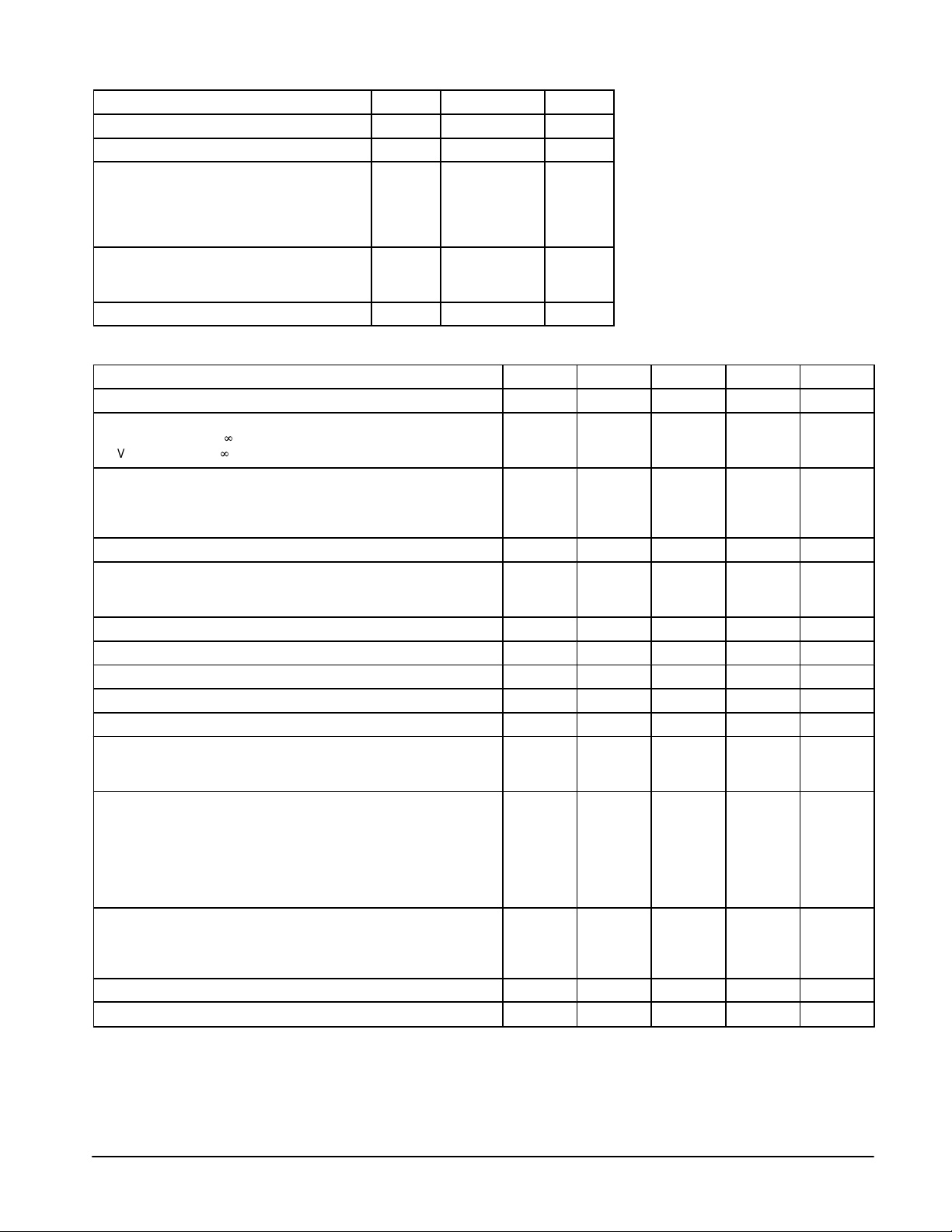
Figure 4. Trigger Pulse Width
150
125
100
75
50
PW, PULSE WIDTH (ns min)
25
0
V
, MINIMUM TRIGGER VOLTAGE (x VCC = Vdc)
T (min)
Figure 6. High Output Voltage
2.0
1.8
1.6
1.4
1.2
(Vdc)
OH
1.0
–V
0.8
CC
V
0.6
0.4
0.2
0
1.0
2.0 5.0 10 20 50 100
25°C
I
Source
0°C
25°C
5.0 V ≤ VCC ≤ 15 V
(mA)
70°C
0.30.20.10
0.4
Figure 5. Supply Current
10
25°C
8.0
6.0
4.0
, SUPPLY CURRENT (mA)
CC
2.0
I
0
VCC, SUPPLY VOLTAGE (Vdc)
Figure 7. Low Output Voltage
@ VCC = 5.0 Vdc
10
I
Sink
25°C
(mA)
1.0
0.1
, LOW OUTPUT VOL TAGE (Vdc)
OL
V
0.01
1.0 2.0 5.0 10 20 50 100
155.0 10
Figure 8. Low Output Voltage
@ VCC = 10 Vdc
10
1.0
0.1
, LOW OUTPUT VOL TAGE (Vdc)
OL
V
0.01
1.0
2.0 5.0 10 20 50 100
I
(mA)
Sink
MOTOROLA ANALOG IC DEVICE DATA
25°C
, LOW OUTPUT VOL TAGE (Vdc)
OL
V
10
1.0
0.1
0.01
Figure 9. Low Output Voltage
@ VCC = 15 Vdc
25°C
1.0
2.0 5.0 10 20 50 100
I
(mA)
Sink
3
Page 4
MC1455, B
(
)
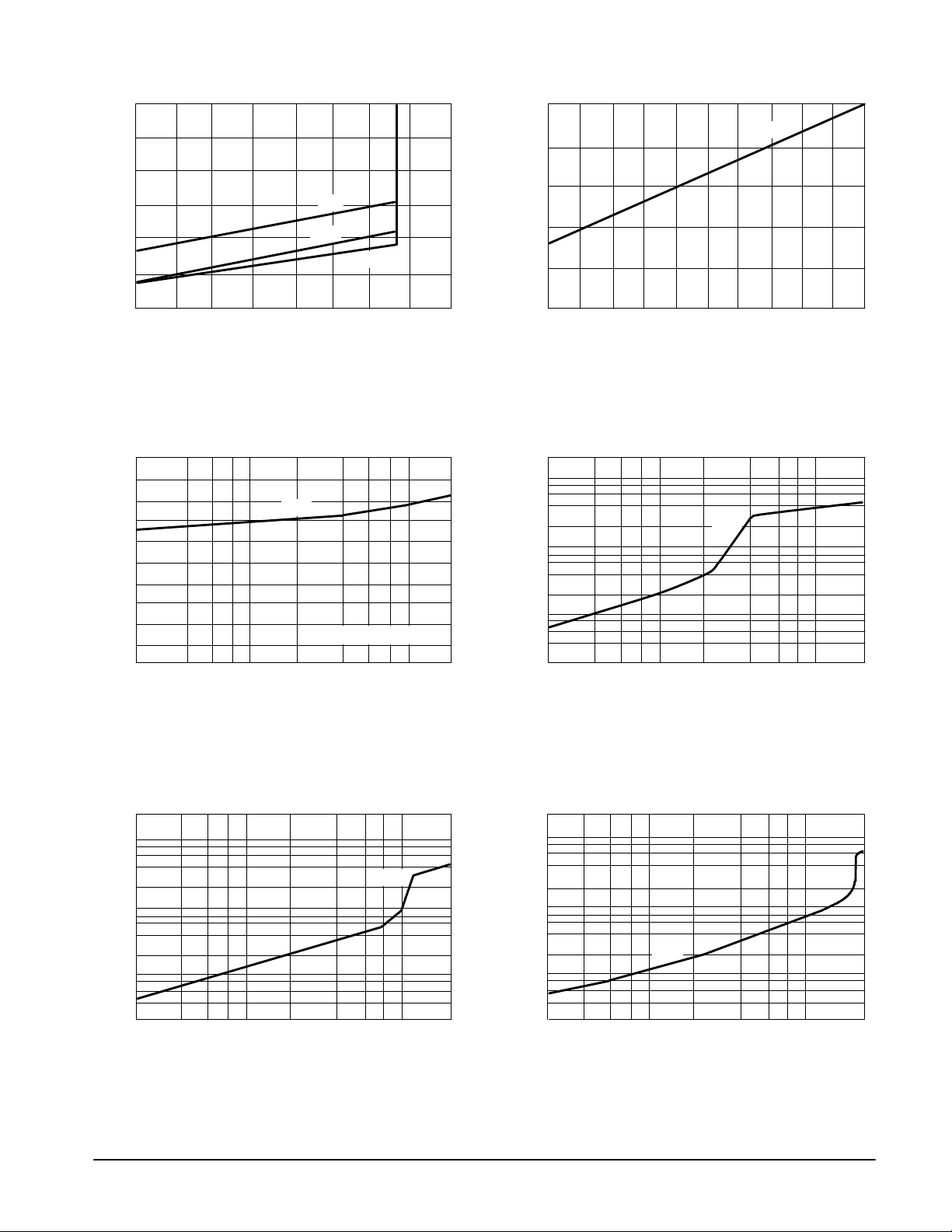
Figure 10. Delay Time versus Supply Voltage
1.015
1.010
1.005
1.000
0.995
, DELAY TIME NORMALIZED
d
0.990
t
0.985
0101510 20
5.0
VCC, SUPPLY VOLTAGE (Vdc)
300
250
200
Figure 11. Delay T ime versus Temperature
1.015
1.010
1.005
1.000
0.995
, DELAY TIME NORMALIZED
d
0.990
t
0.985
–75 –50 –25 0 25 50 75 100 125
Figure 12. Propagation Delay
versus Trigger Voltage
TA, AMBIENT TEMPERATURE (°C)
150
100
, PROPAGATION DELAY TIME (ns)t
pd
50
0°C
70°C
0
0
V
T
25°C
0.1 0.2 0.3 0.4
, MINIMUM TRIGGER VOLTAGE (x VCC = Vdc)
min
4
MOTOROLA ANALOG IC DEVICE DATA
Page 5

MC1455, B
Figure 13. Representative Circuit Schematic
Control Voltage
Threshold
V
CC
Comparator
Trigger
Comparator
1.0 k4.7 k 830 4.7 k
5.0 k
Flip–Flop Output
6.8 k
Threshold
10 k
Trigger
Reset
Reset
Discharge
Gnd
Discharge
100 k
100
GENERAL OPERATION
The MC1455 is a monolithic timing circuit which uses an
external resistor – capacitor network as its timing element. It
can be used in both the monostable (one–shot) and astable
modes with frequency and duty cycle controlled by the
capacitor and resistor values. While the timing is dependent
upon the external passive components, the monolithic circuit
provides the starting circuit, voltage comparison and other
functions needed for a complete timing circuit. Internal to the
integrated circuit are two comparators, one for the input
signal and the other for capacitor voltage; also a flip–flop and
digital output are included. The comparator reference
voltages are always a fixed ratio of the supply voltage thus
providing output timing independent of supply voltage.
Monostable Mode
In the monostable mode, a capacitor and a single resistor
are used for the timing network. Both the threshold terminal
and the discharge transistor terminal are connected together
in this mode (refer to circuit in Figure 14). When the input
voltage to the trigger comparator falls below 1/3 VCC, the
comparator output triggers the flip–flop so that its output sets
low. This turns the capacitor discharge transistor “off” and
drives the digital output to the high state. This condition
allows the capacitor to charge at an exponential rate which is
set by the RC time constant. When the capacitor voltage
reaches 2/3 VCC, the threshold comparator resets the
flip–flop. This action discharges the timing capacitor and
returns the digital output to the low state. Once the flip–flop
has been triggered by an input signal, it cannot be retriggered
7.0 k
3.9 k
Output
5.0 k
5.0 k
c b
4.7 k
e
c
220
4.7 k
b
until the present timing period has been completed. The time
that the output is high is given by the equation t = 1.1 RA C.
Various combinations of R and C and their associated times
are shown in Figure 16. The trigger pulse width must be less
than the timing period.
A reset pin is provided to discharge the capacitor, thus
interrupting the timing cycle. As long as the reset pin is low,
the capacitor discharge transistor is turned “on” and prevents
the capacitor from charging. While the reset voltage is
applied the digital output will remain the same. The reset pin
should be tied to the supply voltage when not in use.
Figure 14. Monostable Circuit
+VCC (5.0 V to 15 V)
R
L
R
L
Output
3
2
Trigger
Reset
4
MC1455
V
CC
8
Discharge
7
6
Threshold
5
Control
1
Voltage
0.01
R
C
µ
F
A
MOTOROLA ANALOG IC DEVICE DATA
5
Page 6

MC1455, B
Figure 15. Monostable Waveforms Figure 16. Time Delay
100
10
µ
1.0
0.1
C, CAPACITANCE ( F)
0.01
t = 50 µs/cm
(RA = 10 kΩ, C = 0.01 µF, RL = 1.0 kΩ, VCC = 15 V)
Figure 17. Astable Circuit Figure 18. Astable Waveforms
+VCC (5.0 V to 15 V)
Output
3
Trigger
2
Reset
4
MC1455
R
L
R
L
V
CC
8
7 Discharge
6 Threshold
5
Control
1
Voltage
R
A
R
B
C
Astable Mode
In the astable mode the timer is connected so that it will
retrigger itself and cause the capacitor voltage to oscillate
between 1/3 VCC and 2/3 VCC. See Figure 17.
The external capacitor changes to 2/3 VCC through RA and
RB and discharges to 1/3 VCC through RB. By varying the ratio
of these resistors the duty cycle can be varied. The charge and
discharge times are independent of the supply voltage.
The charge time (output high) is given by:
t1 = 0.695 (RA + RB)
C
The discharge time (output low) is given by:
t2 = 0.695 (RB) C
Thus the total period is given by:
T = t1 + t2 = 0.695 (RA +2RB)
The frequency of oscillation is then:
f =
C
1
=
T
(RA +2RB) C
1.44
and may be easily found as shown in Figure 19.
R
The duty cycle is given by:
DC =
B
RA +2R
B
To obtain the maximum duty cycle RA must be as small as
possible; but it must also be large enough to limit the
0.001
µ
s 100 µs 1.0 ms 10 ms 100 ms 1.0 10 100
10
td, TIME DELAY (s)
µ
s/cm
(RA = 5.1 k
Ω
, C = 0.01 µF, RL = 1.0 kΩ; RB = 3.9 kΩ, VCC = 15 V)
t = 20
discharge current (Pin 7 current) within the maximum rating
of the discharge transistor (200 mA).
The minimum value of RA is given by:
R
A
VCC (Vdc)
≥
I7 (A)
VCC (Vdc)
≥
0.2
Figure 19. Free Running Frequency
100
10
µ
1.0
0.1
C, CAPACITANCE ( F)
0.01
(RA + 2 RB)
0.001
0.1 1.0 10 100 1.0 k 10 k 100 k
f, FREE RUNNING FREQUENCY (Hz)
6
MOTOROLA ANALOG IC DEVICE DATA
Page 7

MC1455, B
APPLICATIONS INFORMATION
Linear V oltage Ramp
In the monostable mode, the resistor can be replaced by a
constant current source to provide a linear ramp voltage. The
capacitor still charges from 0 VCC to 2/3 VCC. The linear ramp
time is given by:
2
t =
V
CC
3
, where I =
1
VCC – VB – V
R
E
BE
If VB is much larger than VBE, then t can be made
independent of VCC.
Figure 20. Linear V oltage Sweep Circuit Figure 21. Missing Pulse Detector
V
CC
Digital
Output
Trigger
Reset 4
3
2
8V
MC1455
1
CC
0.01
7
6
5
µ
F
R
V
E
Sweep
Output
Control
Voltage
E
I
2N4403
or Equiv
C
R1
V
R2
B
Missing Pulse Detector
The timer can be used to produce an output when an input
pulse fails to occur within the delay of the timer. To
accomplish this, set the time delay to be slightly longer than
the time between successive input pulses. The timing cycle is
then continuously reset by the input pulse train until a change
in frequency or a missing pulse allows completion of the
timing cycle, causing a change in the output level.
+VCC (5.0 V to 15 V)
V
CC
Discharge
7
Threshold
Control
6
Voltage
5
0.01
R
A
C
µ
F
2N4403
or Equiv
Output
Input
R
L
Trigger
Reset
48
3
MC1455
2
1
Figure 22. Linear V oltage Ramp Waveforms Figure 23. Missing Pulse Detector Waveforms
µ
(RE = 10 k
s/cm
t = 100
Ω
, R2 = 100 kΩ, R1 = 39 kΩ, C = 0.01 µF, VCC = 15 V) (RA = 2.0 kΩ, RL = 1.0 kΩ, C = 0.01 µF, VCC = 15 V)
t = 500
µ
s/cm
MOTOROLA ANALOG IC DEVICE DATA
7
Page 8

MC1455, B
Pulse Width Modulation
If the timer is triggered with a continuous pulse train in the
monstable mode of operation, the charge time of the
capacitor can be varied by changing the control voltage at
Pin 5. In this manner, the output pulse width can be
modulated by applying a modulating signal that controls the
threshold voltage.
Figure 24. Pulse Width Modulator
+VCC (5.0 V to 15 V)
Figure 25. Pulse Width Modulation Waveforms
Output
Clock
Input
9.1 k
1.0
R
L
3
2
84
6
MC1455
7
2
µ
F
48
MC1455
1
0.01
5
3
0.001
1
µ
27 k
F
5.0 µF
R
A
7
6
5
C
Modulation
Input
(RA = 10 kΩ, C = 0.02 µF, VCC = 15 V)
T est Sequences
Several timers can be connected to drive each other for
sequential timing. An example is shown in Figure 26 where
the sequence is started by triggering the first timer which runs
for 10 ms. The output then switches low momentarily and
starts the second timer which runs for 50 ms and so forth.
t = 0.5 ms/cm
Figure 26. Sequential Timer
VCC (5.0 V to 15 V)
5.0
18.2 k
84
6
7
2
µ
F
µ
F
MC1455
1
5
3
9.1 k
84
6
7
MC1455
2
µ
F
1
27 k
0.01
µ
F 0.01 µF
5
3
0.001
Load
8
Load
Load
MOTOROLA ANALOG IC DEVICE DATA
Page 9

NOTE 2
–T–
SEATING
PLANE
H
58
–B–
14
F
–A–
C
N
D
K
G
0.13 (0.005) B
M
T
MC1455, B
OUTLINE DIMENSIONS
P1 SUFFIX
PLASTIC PACKAGE
CASE 626–05
ISSUE K
L
J
M
M
A
M
NOTES:
1. DIMENSION L TO CENTER OF LEAD WHEN
FORMED PARALLEL.
2. PACKAGE CONTOUR OPTIONAL (ROUND OR
SQUARE CORNERS).
3. DIMENSIONING AND TOLERANCING PER ANSI
Y14.5M, 1982.
DIM MIN MAX MIN MAX
A 9.40 10.16 0.370 0.400
B 6.10 6.60 0.240 0.260
C 3.94 4.45 0.155 0.175
D 0.38 0.51 0.015 0.020
F 1.02 1.78 0.040 0.070
G 2.54 BSC 0.100 BSC
H 0.76 1.27 0.030 0.050
J 0.20 0.30 0.008 0.012
K 2.92 3.43 0.115 0.135
L 7.62 BSC 0.300 BSC
M ––– 10 ––– 10
N 0.76 1.01 0.030 0.040
INCHESMILLIMETERS
__
MOTOROLA ANALOG IC DEVICE DATA
9
Page 10

A
C
E
B
A1
MC1455, B
OUTLINE DIMENSIONS
D SUFFIX
PLASTIC PACKAGE
CASE 751–06
(SO–8)
ISSUE T
D
58
0.25MB
1
H
4
e
M
h
X 45
_
q
C
A
SEATING
PLANE
0.10
L
B
SS
A0.25MCB
NOTES:
1. DIMENSIONING AND TOLERANCING PER ASME
Y14.5M, 1994.
2. DIMENSIONS ARE IN MILLIMETER.
3. DIMENSION D AND E DO NOT INCLUDE MOLD
PROTRUSION.
4. MAXIMUM MOLD PROTRUSION 0.15 PER SIDE.
5. DIMENSION B DOES NOT INCLUDE DAMBAR
PROTRUSION. ALLOWABLE DAMBAR
PROTRUSION SHALL BE 0.127 TOTAL IN EXCESS
OF THE B DIMENSION AT MAXIMUM MATERIAL
CONDITION.
MILLIMETERS
DIM MIN MAX
A 1.35 1.75
A1 0.10 0.25
B 0.35 0.49
C 0.19 0.25
D 4.80 5.00
E
3.80 4.00
1.27 BSCe
H 5.80 6.20
h
0.25 0.50
L 0.40 1.25
0 7
q
__
10
MOTOROLA ANALOG IC DEVICE DATA
Page 11

MC1455, B
NOTES
MOTOROLA ANALOG IC DEVICE DATA
11
Page 12

MC1455, B
Motorola reserves the right to make changes without further notice to any products herein. Motorola makes no warranty , representation or guarantee regarding
the suitability of its products for any particular purpose, nor does Motorola assume any liability arising out of the application or use of any product or circuit, and
specifically disclaims any and all liability, including without limitation consequential or incidental damages. “T ypical” parameters which may be provided in Motorola
data sheets and/or specifications can and do vary in different applications and actual performance may vary over time. All operating parameters, including “Typicals”
must be validated for each customer application by customer’s technical experts. Motorola does not convey any license under its patent rights nor the rights of
others. Motorola products are not designed, intended, or authorized for use as components in systems intended for surgical implant into the body, or other
applications intended to support or sustain life, or for any other application in which the failure of the Motorola product could create a situation where personal injury
or death may occur. Should Buyer purchase or use Motorola products for any such unintended or unauthorized application, Buyer shall indemnify and hold Motorola
and its officers, employees, subsidiaries, affiliates, and distributors harmless against all claims, costs, damages, and expenses, and reasonable attorney fees
arising out of, directly or indirectly, any claim of personal injury or death associated with such unintended or unauthorized use, even if such claim alleges that
Motorola was negligent regarding the design or manufacture of the part. Motorola and are registered trademarks of Motorola, Inc. Motorola, Inc. is an Equal
Opportunity/Affirmative Action Employer.
How to reach us:
USA/EUROPE /Locations Not Listed: Motorola Literature Distribution; JAPAN: Motorola Japan Ltd.; SPD, Strategic Planning Office, 141,
P.O. Box 5405, Denver, Colorado 80217. 1–303–675–2140 or 1–800–441–2447 4–32–1 Nishi–Gotanda, Shinagawa–ku, Tokyo, Japan. 81–3–5487–8488
Customer Focus Center: 1–800–521–6274
Mfax: RMFAX0@email.sps.mot.com – TOUCHTONE 1–602–244–6609 ASIA/PACIFIC: Motorola Semiconductors H.K. Ltd.; Silicon Harbour Centre,
Motorola Fax Back System – US & Canada ONLY 1–800–774–1848 2, Dai King Street, Tai Po Industrial Estate, Tai Po, N.T., Hong Kong.
HOME PAGE: http://motorola.com/sps/
12
– http://sps.motorola.com/mfax/ 852–26668334
◊
MOTOROLA ANALOG IC DEVICE DATA
Mfax is a trademark of Motorola, Inc.
MC1455/D
 Loading...