

Page 1
MOTOROLA CMOS LOGIC DATA
1
MC14549B MC14559B
The MC14549B and MC14559B successive approximation registers are
8–bit registers providing all the digital control and storage necessary for
successive approximation analog–to–digital conversion systems. These
parts d iffer in only one control i nput. T he Master Reset ( MR) on the
MC14549B is required in the cascaded mode when more than 8 bits are
desired. The Feed Forward (FF) of the MC14559B is used for register
shortening where End–of–Conversion (EOC) is required after less than eight
cycles.
Applications for the MC14549B and MC14559B include analog–to–digital
conversion, with serial and parallel outputs.
• Totally Synchronous Operation
• All Outputs Buffered
• Single Supply Operation
• Serial Output
• Retriggerable
• Compatible with a Variety of Digital and Analog Systems such as the
MC1408 8–Bit D/A Converter
• All Control Inputs Positive–Edge Triggered
• Supply Voltage Range = 3.0 Vdc to 18 Vdc
• Capable of Driving Two Low–Power TTL Loads, One Low–Power
Schottky TTL Load or Two HTL Loads Over the Rated Temperature
Range
• Chip Complexity: 488 FETs or 122 Equivalent Gates
MAXIMUM RATINGS* (Voltages referenced to V
SS
)
Rating
Symbol Value Unit
DC Supply Voltage V
DD
– 0.5 to + 18 Vdc
Input Voltage, All Inputs V
in
– 0.5 to VDD + 0.5 Vdc
DC Input Current, per Pin I
in
± 10 mAdc
Power Dissipation, per Package† P
D
500 mW
Operating Temperature Range T
A
– 55 to + 125
_
C
Storage Temperature Range T
stg
– 65 to + 150
_
C
*Maximum Ratings are those values beyond which damage to the device may occur.
†Temperature Derating:
“P and D/DW” Packages: – 7.0 mW/C From 65_C To 125_C Ceramic
“L” Packages: – 12 mW/_C From 100_C To 125_C
SC SC(
t–1
) MR MR(
t–1
) Clock Action
X X X X None
X X 1 X Reset
1 0 0 0 Start
Conversion
1 X 0 1 Start
Conversion
1 1 0 0 Continue
Conversion
0 X 0 X Continue
Previous
Operation
TRUTH TABLES
MC14549B
X = Don’t Care t–1 = State at Previous Clock
SC SC(
t–1
) EOC Clock Action
X X X None
1 0 0 Start
Conversion
X 1 0 Continue
Conversion
0 0 0 Continue
Conversion
0 X 1 Retain
Conversion
Result
1 X 1 Start
Conversion
MC14559B
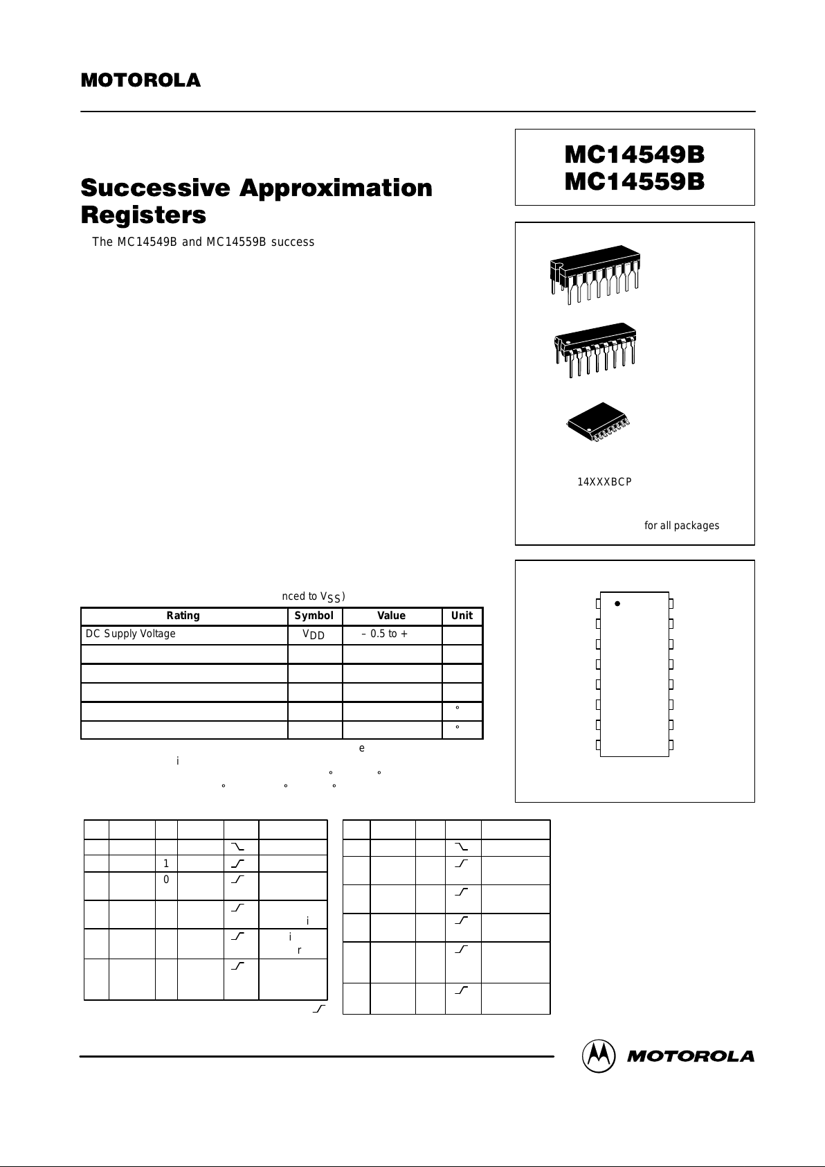
SEMICONDUCTOR TECHNICAL DATA
Motorola, Inc. 1995
REV 3
1/94
L SUFFIX
CERAMIC
CASE 620
ORDERING INFORMATION
MC14XXXBCP Plastic
MC14XXXBCL Ceramic
MC14XXXBDW SOIC
TA = – 55° to 125°C for all packages.
P SUFFIX
PLASTIC
CASE 648
DW SUFFIX
SOIC
CASE 751G
PIN ASSIGNMENT
13
14
15
16
9
10
11
125
4
3
2
1
8
7
6
Q0
Q1
Q2
Q3
V
DD
SC
*
EOC
Q7
Q6
Q5
Q4
V
SS
C
D
S
out
*For MC14549B Pin 10 is MR input.
For MC14559B Pin 10 is FF input.
Page 2
MOTOROLA CMOS LOGIC DATAMC14549B MC14559B
2
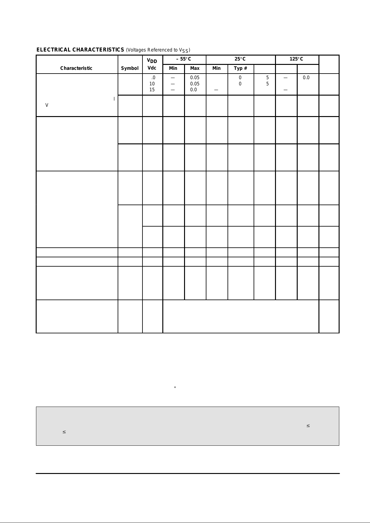
ELECTRICAL CHARACTERISTICS (Voltages Referenced to V
SS
)
V
DD
– 55_C 25_C 125_C
Characteristic
Symbol
DD
Vdc
Min Max Min Typ # Max Min Max
Unit
Output Voltage “0” Level
Vin = VDD or 0
V
OL
5.0
10
15
—
—
—
0.05
0.05
0.05
—
—
—
0
0
0
0.05
0.05
0.05
—
—
—
0.05
0.05
0.05
Vdc
“1” Level
Vin = 0 or V
DD
V
OH
5.0
10
15
4.95
9.95
14.95
—
—
—
4.95
9.95
14.95
5.0
10
15
—
—
—
4.95
9.95
14.95
—
—
—
Vdc
Input Voltage # “0” Level
(VO = 4.5 or 0.5 Vdc)
(VO = 9.0 or 1.0 Vdc)
(VO = 13.5 or 1.5 Vdc)
V
IL
5.0
10
15
—
—
—
1.5
3.0
4.0
—
—
—
2.25
4.50
6.75
1.5
3.0
4.0
—
—
—
1.5
3.0
4.0
Vdc
“1” Level
(VO = 0.5 or 4.5 Vdc)
(VO = 1.0 or 9.0 Vdc)
(VO = 1.5 or 13.5 Vdc)
V
IH
5.0
10
15
3.5
7.0
11
—
—
—
3.5
7.0
11
2.75
5.50
8.25
—
—
—
3.5
7.0
11
—
—
—
Vdc
Output Drive Current
(VOH = 2.5 Vdc) Source
(VOH = 4.6 Vdc)
(VOH = 9.5 Vdc)
(VOH = 13.5 Vdc)
I
OH
5.0
5.0
10
15
– 1.2
– 0.25
– 0.62
– 1.8
—
—
—
—
– 1.0
– 0.2
– 0.5
– 1.5
– 1.7
– 0.36
– 0.9
– 3.5
—
—
—
—
– 0.7
– 0.14
– 0.35
– 1.1
—
—
—
—
mAdc
(VOL = 0.4 Vdc) Sink
(VOL = 0.5 Vdc) Q Outputs
(VOL = 1.5 Vdc)
I
OL
5.0
10
15
1.28
3.2
8.4
—
—
—
1.02
2.6
6.8
1.76
4.5
17.6
—
—
—
0.72
1.8
4.8
—
—
—
mAdc
(VOL = 0.4 Vdc) Sink
(VOL = 0.5 Vdc) Pin 5, 11 only
(VOL = 1.5 Vdc)
5.0
10
15
0.64
1.6
4.2
—
—
—
0.51
1.3
3.4
0.88
2.25
8.8
—
—
—
0.36
0.9
2.4
—
—
—
mAdc
Input Current I
in
15 — ±0.1 — ±0.00001 ±0.1 — ±1.0 µAdc
Input Capacitance C
in
— — — — 5.0 7.5 — — pF
Quiescent Current
(Per Package)
(Clock = 0 V,
Other Inputs = V
DD
or 0 V, I
out
= 0 µA)
I
DD
5.0
10
15
—
—
—
5.0
10
20
—
—
—
0.005
0.010
0.015
5.0
10
20
—
—
—
150
300
600
µAdc
Total Supply Current**†
(Dynamic plus Quiescent,
Per Package)
(CL = 50 pF on all outputs, all
buffers switching)
I
T
5.0
10
15
IT = (0.8 µA/kHz) f + I
DD
IT = (1.6 µA/kHz) f + I
DD
IT = (2.4 µA/kHz) f + I
DD
µAdc
#Noise immunity specified for worst–case input combination.
Noise Margin for both “1” and “0” level = 1.0 V min @ VDD = 5.0 V
= 2.0 V min @ VDD = 10 V
= 2.5 V min @ VDD = 15 V
†To calculate total supply current at loads other than 50 pF:
IT(CL) = IT(50 pF) + 3.5 x 10⁻³ (CL = 50) VDDf
where: IT is in µA (per package), CL in pF, VDD in V, and f in kHz is input frequency.
**The formulas given are for the typical characteristics only at 25_C.
This device contains circuitry to protect the inputs against damage due to high static voltages or electric fields; however, it
is advised that normal precautions be taken to avoid application of any voltage higher than maximum rated voltages to this
high impedance circuit. For proper operation it is recommended that Vin and V
out
be constrained to the range VSS v (Vin or
V
out
) v VDD.
Unused inputs must always be tied to an appropriate logic voltage level (e.g., either VSS or VDD).
Page 3
MOTOROLA CMOS LOGIC DATA
3
MC14549B MC14559B
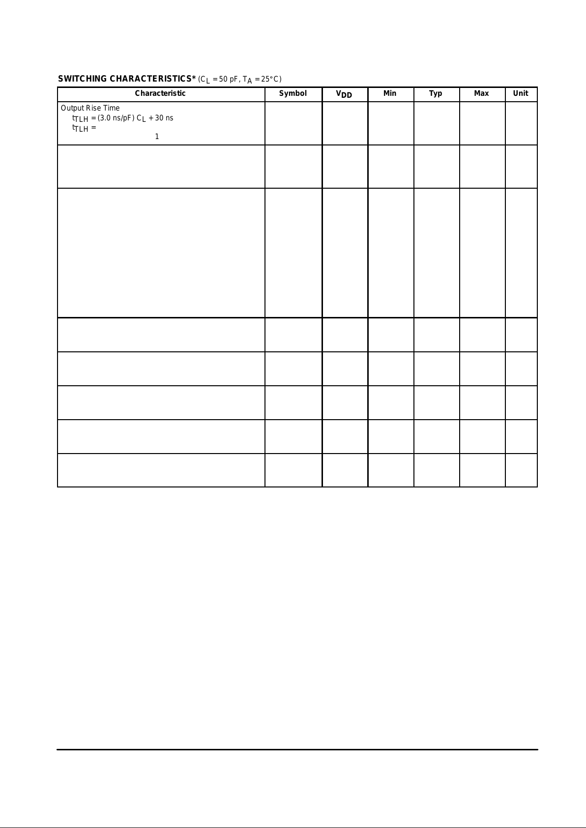
SWITCHING CHARACTERISTICS* (C
L
= 50 pF, TA = 25_C)
Characteristic
Symbol V
DD
Min Typ Max Unit
Output Rise Time
t
TLH
= (3.0 ns/pF) CL + 30 ns
t
TLH
= (1.5 ns/pF) CL + 15 ns
t
TLH
= (1.1 ns/pF) CL + 10 ns
t
TLH
5.0
10
15
—
—
—
180
90
65
360
180
130
ns
Output Fall Time
t
THL
= (1.5 ns/pF) CL + 25 ns
t
THL
= (0.75 ns/pF) CL + 12.5 ns
t
THL
= (0.55 ns/pF) CL + 9.5 ns
t
THL
5.0
10
15
—
—
—
100
50
40
200
100
80
ns
Propagation Delay Time
Clock to Q
t
PLH
, t
PHL
= (1.7 ns/pF) CL + 415 ns
t
PLH
, t
PHL
= (0.66 ns/pF) CL + 177 ns
t
PLH
, t
PHL
= (0.5 ns/pF) CL + 130 ns
Clock to S
out
t
PLH
, t
PHL
= (1.7 ns/pF) CL + 665 ns
t
PLH
, t
PHL
= (0.66 ns/pF) CL + 277 ns
t
PLH
, t
PHL
= (0.5 ns/pF) CL + 195 ns
Clock to EOC
t
PLH
, t
PHL
= (1.7 ns/pF) CL + 215 ns
t
PLH
, t
PHL
= (0.66 ns/pF) CL + 97 ns
t
PLH
, t
PHL
= (0.5 ns/pF) CL + 75 ns
t
PLH
,
t
PHL
5.0
10
15
5.0
10
15
5.0
10
15
—
—
—
—
—
—
—
—
500
210
155
750
310
220
300
130
100
1000
420
310
1500
620
440
600
260
200
ns
SC, D, FF or MR Setup Time t
su
5.0
10
15
250
100
80
125
50
40
—
—
—
ns
Clock Pulse Width t
WH(cl)
5.0
10
15
700
270
200
350
135
100
—
—
—
ns
Pulse Width — D, SC, FF or MR t
WH
5.0
10
15
500
200
160
250
100
80
—
—
—
ns
Clock Rise and Fall Time t
TLH
,
t
THL
5.0
10
15
—
—
— —
15
1.0
0.5
µs
Clock Pulse Frequency f
cl
5.0
10
15
—
—
—
1.5
3.0
4.0
0.8
1.5
2.0
MHz
*The formulas given are for the typical characteristics only.
Page 4

MOTOROLA CMOS LOGIC DATAMC14549B MC14559B
4
SWITCHING TIME TEST CIRCUIT AND WAVEFORMS
1
f
cl
t
WH(cl)
50%
50%
t
su
t
su
t
su
t
WH(D)
t
PHL
t
PLH
50%
50%
90%
10%
t
TLH
t
PLH
t
THL
90%50%
10%
t
TLH
S
out
Q7
D
SC
C
NOTE: Pin 10 = V
SS
C
L
C
L
C
L
C
L
C
L
C
L
C
L
C
L
C
L
C
L
V
DD
V
SS
Q7
Q6
Q5
Q4
Q3
Q2
Q1
Q0
EOC
S
out
C
SC
FF(MR)
D
PROGRAMMABLE
PULSE
GENERATOR
TIMING DIAGRAM
* — Q8 is ninth–bit of serial information available from 8–bit register.
NOTE: Pin 10 = V
SS
INH — Indicates Serial Out is inhibited low.
— Don’t care condition
CLOCK
SC
D
Q7
Q6
Q5
Q4
Q3
Q2
Q1
Q0
EOC
S
out
INHINH Q7
Q6 Q7 Q5 Q3 Q1 Q8*
INHQ6 Q4 Q2 Q0
Page 5

MOTOROLA CMOS LOGIC DATA
5
MC14549B MC14559B
OPERATING CHARACTERISTICS
Both the MC14549B and MC14559B can be operated in
either the “free run” or “strobed operation” mode for conversion schemes with any number of bits. Reliable cascading
and/or recirculating operation can be achieved if the End of
Convert (EOC) output is used as the controlling function,
since with EOC = 0 (and with SC = 1 for MC14549B but
either 1 or 0 for MC14559B) no stable state exists under continual clocked operation. The MC14559B will automatically
recirculate after EOC = 1 during externally strobed operation,
provided SC = 1.
All data and control inputs for these devices are triggered
into the circuit on the positive edge of the clock pulse.
Operation of the various terminals is as follows:
C = Clock — A positive–going transition of the Clock is
required for data on any input to be strobed into the circuit.
SC = Start Convert — A conversion sequence is initiated
on the positive–going transition of the SC input on succeeding clock cycles.
D = Data in — Data on this input (usually from a comparator in A/D applications) is also entered into the circuit on a
positive–going transition of the clock. This input is Schmitt
triggered and synchronized to allow fast response and guaranteed quality of serial and parallel data.
MR = Master Reset (MC14549B Only) — Resets all output to 0 on positive–going transitions of the clock. If removed
while SC = 0, the circuit will remain reset until SC = 1. This
allows easy cascading of circuits.
FF = Feed Forward (MC14559B Only) — Provides register shortening by removing unwanted bits from a system.
For operation with less than 8 bits, tie the output
following
the least significant bit of the circuit to EOC. E.g., for a 6–bit
conversion, tie Q1 to FF; the part will respond as shown in
the timing diagram less two bit times. Not that Q1 and Q0 will
still operate and must be disregarded.
For 8–bit operation, FF is tied to VSS.
For applications with more than 8 but less than 16 bits, use
the basic connections shown in Figure 1. The FF input of the
MC14559B is used to shorten the setup. Tying FF directly to
the least significant bit used in the MC14559B allows EOC to
provide the cascading signal, and results in smooth transition
of serial information from the MC14559B to the MC14549B.
The Serial Out ( S
out
) inhibit structure of the MC14559B
remains inactive one cycle after EOC goes high, while S
out
of
the MC14549B remains inhibited until the second clock cycle
of its operation.
Qn = Data Outputs — After a conversion is initiated the
Q’s on succeeding cycles go high and are then conditionally
reset dependent upon the state of the D input. Once conditionally reset they remain in the proper state until the circuit is
either reset or reinitiated.
EOC = End of Convert — This output goes high on the
negative–going transition of the clock following FF = 1 (for
the MC14559B) or the conditional reset of Q0. This allows
settling of the digital circuitry prior to the End of Conversion
indication. Therefore either level or edge triggering can indicate complete conversion.
S
out
= Serial Out — Transmits conversion in serial fash-
ion. Serial data occurs during the clock period when the corresponding parallel data bit is conditionally reset. Serial Out
is inhibited on the initial period of a cycle, when the circuit is
reset, and on the second cycle after EOC goes high. This
provides efficient operation when cascaded.
Figure 1. 12–Bit Conversion Scheme
†Completion of conversion automatically re–initiates cycle in free run mode.
**Cascading using EOC guaranteed; no stable unfunctional state.
*FF allows EOC to activate as if in 4–stage register.
Q7 Q6 Q5 Q4 Q0 EOC
FF
SC
C
D
S
out
MC14559B
NC
MSB
TO D/A AND PARALLEL DATA
••
**
*
FROM A/D
COMPARATOR
Q7 Q6 Q5
MR
SC
C
D
S
out
MC14549B
LSB
Q4
Q3 Q2 Q1 Q0 EOC
TO D/A AND
PARALLEL DATA
{
EXTERNAL STROBE
FREE RUN MODE
EXTERNAL
CLOCK
1/4 MC14001
SERIAL OUT
(CONTINUAL
UPDATE EVERY
13 CLOCK CYCLES)
Page 6

MOTOROLA CMOS LOGIC DATAMC14549B MC14559B
6
TYPICAL APPLICATIONS
Externally Controlled 6–Bit ADC (Figure 2)
Several features are shown in this application:
• Shortening of the register to six bits by feeding the seventh
output bit into the FF input.
• Continuous conversion, if a continuous signal is applied to
SC.
• Externally controlled updating (the start pulse must be
shorter than the conversion cycle).
• The EOC output indicating that the parallel data are valid
and that the serial output is complete.
Continuously Cycling 8–Bit ADC (Figure 3)
This ADC is running continuously because the EOC signal
is fed back to the SC input, immediately initiating a new cycle
on the next clock pulse.
Continuously Cycling 12–Bit ADC (Figure 4)
Because each successive approximation register (SAR)
has a capability of handling only an eight–bit word, two must
be cascaded to make an ADC with more than eight bits.
When it is necessary to cascade two SAR’s, the second
SAR must have a stable resettable state to remain in while
awaiting a subsequent start signal. However, the first stage
must not have a stable resettable state while recycling, because during switch–on or due to outside influences, the first
stage has entered a reset state, the entire ADC will remain in
a stable non–functional condition.
This 12–bit ADC is continuously recycling. The serial as
well as t he parallel o utputs are updated e very thirteenth
clock pulse. T he EOC pulse indicates the completion of
Figure 2. Externally Controlled 6–Bit ADC
TO DAC
SC
C
S
out
Q7 Q6 Q5
MC14559B
Q4 Q3 Q2 Q1 Q0 EOCFF
Figure 3. Continuously Cycling 8–Bit ADC
TO DAC
SC
C
S
out
Q7 Q6 Q5
MC14559B
Q4 Q3 Q2 Q1 Q0 EOCFF
Page 7

MOTOROLA CMOS LOGIC DATA
7
MC14549B MC14559B
Q7 Q6 Q5
MR
SC
C
S
out
MC14549B
Q4 Q3 Q2 Q1 Q0 EOC
S
out
TO DAC
Q7 Q6 Q5
SC
C S
out
MC14559B
Q4 Q3 Q2 Q1 Q0 EOC
TO DAC
FF
EOC
Figure 4. Continuously Cycling 12–Bit ADC
the 12–bit conversion cycle, the end of the serial output
word, and the validity of the parallel data output.
Externally Controlled 12–Bit ADC (Figure 5)
In this circuit the external pulse starts the first SAR and
simultaneously resets the cascaded second SAR. When Q4
of the first SAR goes high, the second SAR starts conversion, and the first one stops conversion. EOC indicates that
the parallel data are valid and that the serial output is complete. Updating the output data is started with every external
control pulse.
Additional Motorola Parts for Successive
Approximation ADC
Monolithic d igital–to–analog c onverters — The
MC1408/1508 converter has eight–bit resolution and is available with 6, 7, and 8–bit accuracy. The amplifier–compara-
tor block — The MC1407/1507 contains a high s peed
operational amplifier and a high speed comparator with adjustable window.
With these two linear parts it is possible to construct SA–
ADCs with an accuracy of up to eight bits, using as the register one MC14549B or one MC14559B. An additional CMOS
block will be necessary to generate the clock frequency.
Additional information on successive approximation ADC
is found in Motorola Application Note AN–716.
Figure 5. Externally Controlled 12–Bit ADC
Q7 Q6 Q5
MR
SC
C
S
out
MC14549B
Q4 Q3 Q2 Q1 Q0 EOC
S
out
TO DAC
Q7 Q6 Q5
SC
C S
out
MC14559B
Q4 Q3 Q2 Q1 Q0 EOC
TO DAC
FF
EOC
Page 8

MOTOROLA CMOS LOGIC DATAMC14549B MC14559B
8
OUTLINE DIMENSIONS
P SUFFIX
PLASTIC DIP PACKAGE
CASE 648–08
ISSUE R
NOTES:
1. DIMENSIONING AND TOLERANCING PER ANSI
Y14.5M, 1982.
2. CONTROLLING DIMENSION: INCH.
3. DIMENSION L TO CENTER OF LEADS WHEN
FORMED PARALLEL.
4. DIMENSION B DOES NOT INCLUDE MOLD FLASH.
5. ROUNDED CORNERS OPTIONAL.
–A–
B
F
C
S
H
G
D
J
L
M
16 PL
SEATING
1 8
916
K
PLANE
–T–
M
A
M
0.25 (0.010) T
DIM MIN MAX MIN MAX
MILLIMETERSINCHES
A 0.740 0.770 18.80 19.55
B 0.250 0.270 6.35 6.85
C 0.145 0.175 3.69 4.44
D 0.015 0.021 0.39 0.53
F 0.040 0.70 1.02 1.77
G 0.100 BSC 2.54 BSC
H 0.050 BSC 1.27 BSC
J 0.008 0.015 0.21 0.38
K 0.110 0.130 2.80 3.30
L 0.295 0.305 7.50 7.74
M 0 10 0 10
S 0.020 0.040 0.51 1.01
____
L SUFFIX
CERAMIC DIP PACKAGE
CASE 620–10
ISSUE V
NOTES:
1. DIMENSIONING AND TOLERANCING PER
ANSI Y14.5M, 1982.
2. CONTROLLING DIMENSION: INCH.
3. DIMENSION L TO CENTER OF LEAD WHEN
FORMED PARALLEL.
4. DIMENSION F MAY NARROW TO 0.76 (0.030)
WHERE THE LEAD ENTERS THE CERAMIC
BODY.
–A–
–B–
–T–
F
E
G
N
K
C
SEATING
PLANE
16 PLD
S
A
M
0.25 (0.010) T
16 PLJ
S
B
M
0.25 (0.010) T
M
L
DIM MIN MAX MIN MAX
MILLIMETERSINCHES
A 0.750 0.785 19.05 19.93
B 0.240 0.295 6.10 7.49
C ––– 0.200 ––– 5.08
D 0.015 0.020 0.39 0.50
E 0.050 BSC 1.27 BSC
F 0.055 0.065 1.40 1.65
G 0.100 BSC 2.54 BSC
H 0.008 0.015 0.21 0.38
K 0.125 0.170 3.18 4.31
L 0.300 BSC 7.62 BSC
M 0 15 0 15
N 0.020 0.040 0.51 1.01
_ _ _ _
16 9
1 8
Page 9

MOTOROLA CMOS LOGIC DATA
9
MC14549B MC14559B
OUTLINE DIMENSIONS
DW SUFFIX
PLASTIC SOIC PACKAGE
CASE 751G–02
ISSUE A
DIM MIN MAX MIN MAX
INCHESMILLIMETERS
A 10.15 10.45 0.400 0.411
B 7.40 7.60 0.292 0.299
C 2.35 2.65 0.093 0.104
D 0.35 0.49 0.014 0.019
F 0.50 0.90 0.020 0.035
G 1.27 BSC 0.050 BSC
J 0.25 0.32 0.010 0.012
K 0.10 0.25 0.004 0.009
M 0 7 0 7
P 10.05 10.55 0.395 0.415
R 0.25 0.75 0.010 0.029
M
B
M
0.010 (0.25)
NOTES:
1. DIMENSIONING AND TOLERANCING PER ANSI
Y14.5M, 1982.
2. CONTROLLING DIMENSION: MILLIMETER.
3. DIMENSIONS A AND B DO NOT INCLUDE MOLD
PROTRUSION.
4. MAXIMUM MOLD PROTRUSION 0.15 (0.006) PER
SIDE.
5. DIMENSION D DOES NOT INCLUDE DAMBAR
PROTRUSION. ALLOWABLE DAMBAR
PROTRUSION SHALL BE 0.13 (0.005) TOTAL IN
EXCESS OF D DIMENSION AT MAXIMUM
MATERIAL CONDITION.
–A–
–B– P8X
G14X
D16X
SEATING
PLANE
–T–
S
A
M
0.010 (0.25) B
S
T
16 9
81
F
J
R
X 45
_
_ _ _ _
M
C
K
How to reach us:
USA/EUROPE/Locations Not Listed: Motorola Literature Distribution; JAPAN: Nippon Motorola Ltd.; Tatsumi–SPD–JLDC, 6F Seibu–Butsuryu–Center,
P.O. Box 20912; Phoenix, Arizona 85036. 1–800–441–2447 or 602–303–5454 3–14–2 Tatsumi Koto–Ku, Tokyo 135, Japan. 03–81–3521–8315
MFAX: RMFAX0@email.sps.mot.com – TOUCHTONE 602–244–6609 ASIA/PACIFIC: Motorola Semiconductors H.K. Ltd.; 8B Tai Ping Industrial Park,
INTERNET: http://Design–NET.com 51 Ting Kok Road, Tai Po, N.T., Hong Kong. 852–26629298
Motorola reserves the right to make changes without further notice to any products herein. Motorola makes no warranty , representation or guarantee regarding
the suitability of its products for any particular purpose, nor does Motorola assume any liability arising out of the application or use of any product or circuit,
and specifically disclaims any and all liability, including without limitation consequential or incidental damages. “Typical” parameters which may be provided
in Motorola data sheets and/or specifications can and do vary in different applications and actual performance may vary over time. All operating parameters,
including “Typicals” must be validated for each customer application by customer’s technical experts. Motorola does not convey any license under its patent
rights nor the rights of others. Motorola products are not designed, intended, or authorized for use as components in systems intended for surgical implant
into the body, or other applications intended to support or sustain life, or for any other application in which the failure of the Motorola product could create a
situation where personal injury or death may occur. Should Buyer purchase or use Motorola products for any such unintended or unauthorized application,
Buyer shall indemnify and hold Motorola and its officers, employees, subsidiaries, affiliates, and distributors harmless against all claims, costs, damages, and
expenses, and reasonable attorney fees arising out of, directly or indirectly, any claim of personal injury or death associated with such unintended or
unauthorized use, even if such claim alleges that Motorola was negligent regarding the design or manufacture of the part. Motorola and are registered
trademarks of Motorola, Inc. Motorola, Inc. is an Equal Opportunity/Affirmative Action Employer .
MC14549B/D
*MC14549B/D*
◊
 Loading...