

Page 1
MOTOROLA CMOS LOGIC DATA
1
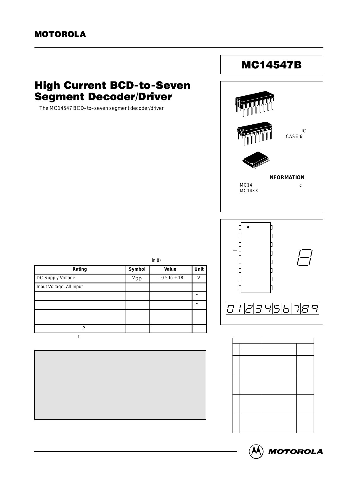
MC14547B
The MC14547 BCD–to–seven segment decoder/driver is constructed with
complementary MOS (CMOS) enhancement mode devices and NPN bipolar
output drivers in a single monolithic structure. The circuit provides the
functions of an 8421 BCD–to–seven segment decoder with high output drive
capability. Blanking (BI), can be used to turn off or pulse modulate the
brightness o f the d isplay. The M C14547 can d rive seven–segment
light–emitting diodes (LED), incandescent, fluorescent or gas discharge
readouts either directly or indirectly.
Applications include instrument (e.g., counter, DVM, etc.) display driver,
computer/calculator display driver, cockpit display driver, and various clock,
watch, and timer uses.
• High Current Sourcing Outputs (Up to 65 mA)
• Low Logic Circuit Power Dissipation
• Supply Voltage Range = + 3.0 V to + 18 V
• Blanking Input
• Readout Blanking on All Illegal Combinations
• Lamp Intensity Modulation Capability
• Multiplexing Capability
• Capable of Driving Two Low–Power TTL Loads, One Low–Power
Schottky TTL Load or Two HTL Loads over the Rated Temperature
Range
• Use MC14511B for Applications Requiring Data Latches
MAXIMUM RATINGS* (Voltages referenced to V
SS
, Pin 8)
Rating
Symbol Value Unit
DC Supply Voltage V
DD
– 0.5 to + 18 V
Input Voltage, All Inputs V
in
– 0.5 to VDD + 0.5 V
Operating Temperature Range T
A
– 55 to + 125
_
C
Storage Temperature Range T
stg
– 65 to + 150
_
C
Maximum Continuous Output Drive
Current (Source) per Output
I
OHmax
65 mA
Maximum Continuous Power Dissipation P
D
1200* mW
*Maximum Ratings are those values beyond which damage to the device may occur.
*See Power Derating Curve Figure 1.
This device contains circuitry to protect the inputs against damage
due to high static voltages or electric fields; however, it is advised that
normal precautions be taken to avoid application of any voltage higher
than maximum rated voltages to this high-impedance circuit. A destructive high current mode may occur if Vin and V
out
is not constrained to
the range VSS ≤ (Vin or V
out
) ≤ VDD.
Due to the sourcing capability of this circuit, damage can occur to the
device if VDD is applied, and the outputs are shorted to VSS and are at a
logical 1 (See Maximum Ratings).
Unused inputs must always be tied to an appropriate logic voltage
level (e.g., either VSS or VDD).
Inputs Outputs
BI
D C B A a b c d e f g Display
0 X X X X 0 0 0 0 0 0 0 Blank
1 0 0 0 0 1 1 1 1 1 1 0 0
1 0 0 0 1 0 1 1 0 0 0 0 1
1 0 0 1 0 1 1 0 1 1 0 1 2
1 0 0 1 1 1 1 1 1 0 0 1 3
1 0 1 0 0 0 1 1 0 0 1 1 4
1 0 1 0 1 1 0 1 1 0 1 1 5
1 0 1 1 0 0 0 1 1 1 1 1 6
1 0 1 1 1 1 1 1 0 0 0 0 7
1 1 0 0 0 1 1 1 1 1 1 1 8
1 1 0 0 1 1 1 1 0 0 1 1 9
1 1 0 1 0 0 0 0 0 0 0 0 Blank
1 1 0 1 1 0 0 0 0 0 0 0 Blank
1 1 1 0 0 0 0 0 0 0 0 0 Blank
1 1 1 0 1 0 0 0 0 0 0 0 Blank
1 1 1 1 0 0 0 0 0 0 0 0 Blank
1 1 1 1 1 0 0 0 0 0 0 0 Blank
X = Don’t care
TRUTH TABLE
SEMICONDUCTOR TECHNICAL DATA
Motorola, Inc. 1995
REV 3
1/94
0 1 2 3 4 5 6 7 8 9
DISPLAY
L SUFFIX
CERAMIC
CASE 620
ORDERING INFORMATION
MC14XXXBCP Plastic
MC14XXXBCL Ceramic
MC14XXXBDW SOIC
TA = – 55° to 125°C for all packages.
P SUFFIX
PLASTIC
CASE 648
DW SUFFIX
SOIC
CASE 751G
13
14
15
16
9
10
11
125
4
3
2
1
8
7
6
b
a
g
f
V
DD
e
d
c
BI
NC
C
B
V
SS
A
D
NC
a
b
c
d
e
f
g
Page 2
MOTOROLA CMOS LOGIC DATAMC14547B
2
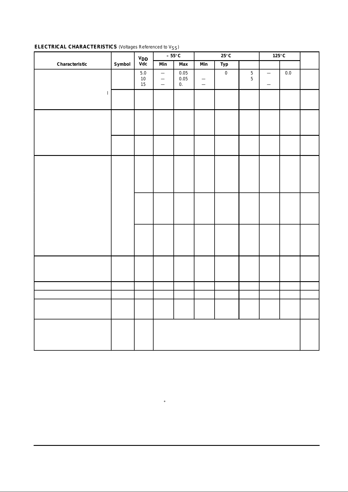
ELECTRICAL CHARACTERISTICS (Voltages Referenced to V
SS
)
V
– 55_C 25_C 125_C
Characteristic
Symbol
V
DD
Vdc
Min Max Min Typ # Max Min Max
Unit
Output Voltage “0” Level
Vin = VDD or 0
V
OL
5.0
10
15
—
—
—
0.05
0.05
0.05
—
—
—
0
0
0
0.05
0.05
0.05
—
—
—
0.05
0.05
0.05
Vdc
“1” Level
Vin = 0 or V
DD
V
OH
5.0
10
15
4.1
9.1
14.1
—
—
—
4.4
9.4
14.4
4.6
9.6
14.6
—
—
—
4.3
9.3
14.4
—
—
—
Vdc
Input Voltage # “0” Level
(VO = 3.8 or 0.5 Vdc)
(VO = 8.8 or 1.0 Vdc)
(VO = 13.8 or 1.5 Vdc)
V
IL
5.0
10
15
—
—
—
1.5
3.0
4.0
—
—
—
2.25
4.50
6.75
1.5
3.0
4.0
—
—
—
1.5
3.0
4.0
Vdc
(VO = 0.5 or 3.8 Vdc)
(VO = 1.0 or 8.8 Vdc)
(VO = 1.5 or 13.8 Vdc)
V
IH
5.0
10
15
3.5
7.0
11
—
—
—
3.5
7.0
11
2.75
5.50
8.25
—
—
—
3.5
7.0
11
—
—
—
Vdc
Output Drive Voltage
(IOH = 5.0 mA) Source
(IOH = 10 mA)
(IOH = 20 mA)
(IOH = 40 mA)
(IOH = 65 mA)
V
OH
5.0 4.0
—
3.8
—
3.1
—
—
—
—
4.2
4.1
3.9
3.7
3.2
4.3
4.3
4.2
4.0
3.7
—
—
—
—
—
4.3
—
4.0
—
3.0
—
—
—
—
—
Vdc
(IOH = 5.0 mA)
(IOH = 10 mA)
(IOH = 20 mA)
(IOH = 40 mA)
(IOH = 65 mA)
10 9.1
—
8.8
—
8.4
—
—
—
—
—
9.2
9.1
9.0
8.9
8.5
9.3
9.3
9.2
9.0
8.8
—
—
—
—
—
9.3
—
9.2
—
8.1
—
—
—
—
—
Vdc
(IOH = 5.0 mA)
(IOH = 10 mA)
(IOH = 20 mA)
(IOH = 40 mA)
(IOH = 65 mA)
15 14
—
13.8
—
13.5
—
—
—
—
—
14.2
14.1
14.0
13.8
13.5
14.3
14.3
14.2
14.0
13.7
—
—
—
—
—
14.4
—
14.2
—
13.3
—
—
—
—
—
Vdc
Output Drive Current
(VOL = 0.4 Vdc) Sink
(VOL = 0.5 Vdc)
(VOL = 1.5 Vdc)
I
OL
5.0
10
15
0.32
0.80
2.10
—
—
—
0.26
0.65
1.7
0.44
1.13
4.4
—
—
—
0.18
0.45
1.2
—
—
—
mAdc
Input Current I
in
15 — ±0.1 — ±0.00001 ±0.1 — ±1.0 µAdc
Input Capacitance C
in
— — — — 5.0 7.5 — — pF
Quiescent Current
(Per Package) Vin = 0 or VDD,
I
out
= 0 µA
I
DD
5.0
10
15
—
—
—
5.0
10
20
—
—
—
0.005
0.010
0.015
5.0
10
20
—
—
—
150
300
600
µAdc
Total Supply Current**†
(Dynamic plus Quiescent,
Per Package)
(CL = 50 pF on all outputs, all
buffers switching)
I
T
5.0
10
15
IT = (1.9 µA/kHz) f + I
DD
IT = (3.8 µA/kHz) f + I
DD
IT = (5.7 µA/kHz) f + I
DD
µAdc
#Noise immunity specified for worst input combination.
Noise Margin for both “1” and “0” level = 1.0 V min @ VDD = 5.0 V
= 2.0 V min @ VDD = 10 V
= 2.5 V min @ VDD = 15 V
†To calculate total supply current at loads other than 50 pF:
IT(CL) = IT(50 pF) + 3.5 x 10⁻³ (CL – 50) VDDf
where: IT is in µA (per package), CL in pF, VDD in V, and f in kHz is input frequency.
**The formulas given are for the typical characteristics only at 25_C.
Page 3
MOTOROLA CMOS LOGIC DATA
3
MC14547B
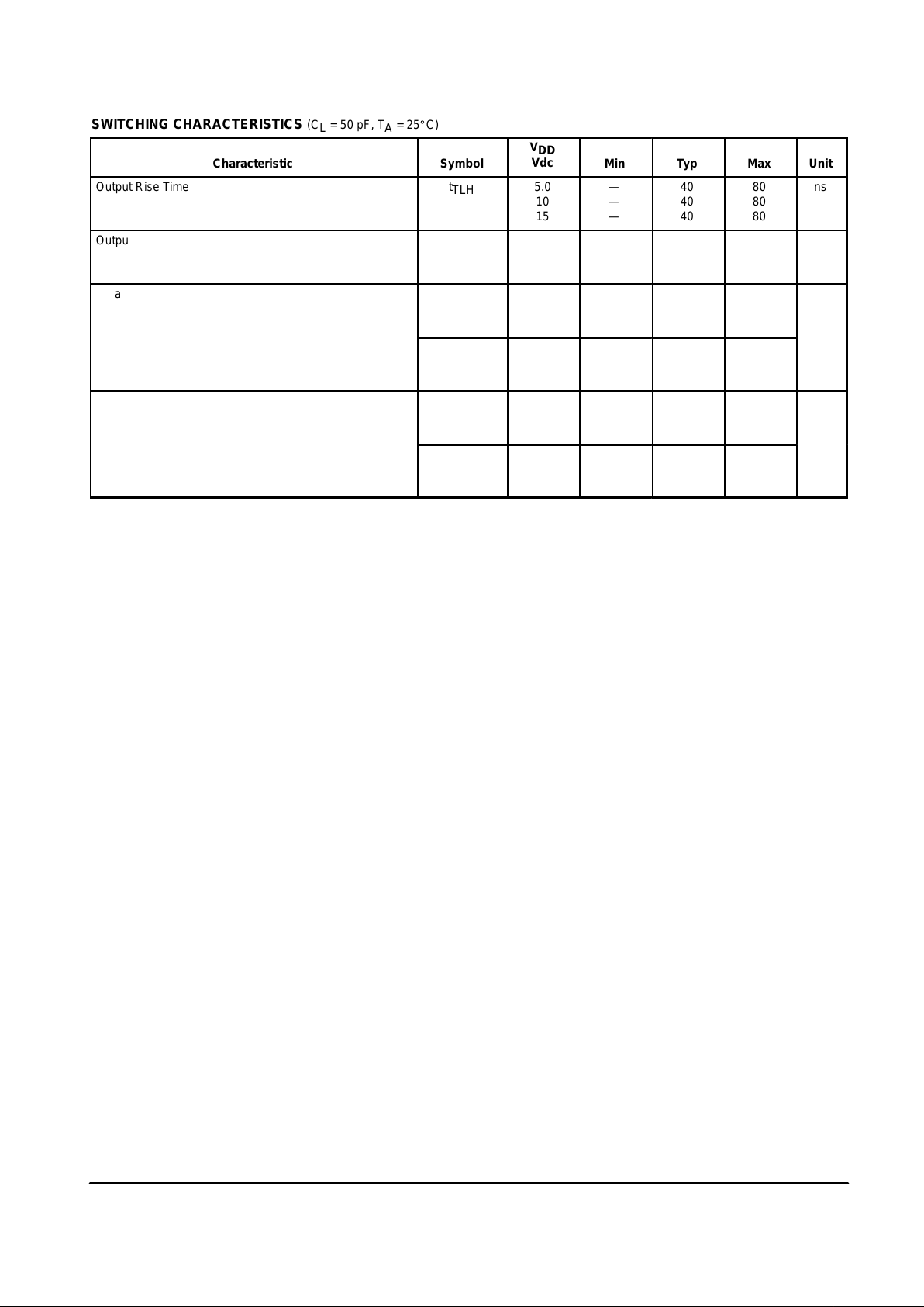
SWITCHING CHARACTERISTICS (C
L
= 50 pF, TA = 25_C)
Characteristic
Symbol
V
DD
Vdc
Min Typ Max Unit
Output Rise Time t
TLH
5.0
10
15
—
—
—
40
40
40
80
80
80
ns
Output Fall Time t
THL
5.0
10
15
—
—
—
125
75
70
250
150
140
ns
Data Propagation Delay Time
t
PLH
5.0
10
15
—
—
—
750
300
200
1500
600
400
ns
t
PHL
5.0
10
15
—
—
—
750
300
200
1500
600
400
Blank Propagation Delay Time
t
PLH
5.0
10
15
—
—
—
750
300
200
1500
600
400
ns
t
PHL
5.0
10
15
—
—
—
500
250
170
1000
500
340
Page 4

MOTOROLA CMOS LOGIC DATAMC14547B
4
LOGIC DIAGRAM
A 7
B 1
C 2
D 6
14 g
15 f
9 e
10 d
11 c
12 b
13 a
4
BI
1200
1000
800
600
400
200
0
175150125100755025
TA, AMBIENT TEMPERATURE (0
°
C)
Figure 1. Ambient Temperature Power Derating
P
D
, MAXIMUM POWER DISSIPATION (mW)
PER PACKAGE
(L) CERAMIC
(P) PDIP
(D) SOIC
410 mW (L)
230 mW (P)
150 mW (D)
Page 5

MOTOROLA CMOS LOGIC DATA
5
MC14547B
CONNECTIONS TO VARIOUS DISPLAY READOUTS
LIGHT EMITTING DIODE (LED) READOUT
INCANDESCENT READOUT LIGHT–EMITTING DIODE (LED) READOUT
USING A ZENER DIODE TO REPLACE DROPPING RESISTORS
*VZD should be set at VDD – 1.3 V – V
LED
. Wattage of zener diode
must be calculated for number of segments and worst–case
conditions.
**A filament pre–warm resistor is recommended to reduce filament
thermal shock and increase the effective cold resistance of the
filament.
GAS DISCHARGE READOUT
FLUORESCENT READOUT
(Caution: Absolute maximum
working voltage = 18.0 V)
V
DD
V
SS
COMMON
CATHODE LED
≈
1.7 V
V
DD
V
SS
COMMON
ANODE LED
≈
1.7 V
V
DD
V
SS
V
DD
V
SS
COMMON
CATHODE LED
V
DD
* *
V
SS
VZD*
V
DD
V
SS
APPROPRIATE
VOLTAGE
V
DD
V
SS
DIRECT
(LOW BRIGHTNESS)
FILAMENT
SUPPLY
VSS OR APPROPRIATE
VOLTAGE BELOW VSS.
Page 6

MOTOROLA CMOS LOGIC DATAMC14547B
6
OUTLINE DIMENSIONS
P SUFFIX
PLASTIC DIP PACKAGE
CASE 648–08
ISSUE R
NOTES:
1. DIMENSIONING AND TOLERANCING PER ANSI
Y14.5M, 1982.
2. CONTROLLING DIMENSION: INCH.
3. DIMENSION L TO CENTER OF LEADS WHEN
FORMED PARALLEL.
4. DIMENSION B DOES NOT INCLUDE MOLD FLASH.
5. ROUNDED CORNERS OPTIONAL.
–A–
B
F
C
S
H
G
D
J
L
M
16 PL
SEATING
1 8
916
K
PLANE
–T–
M
A
M
0.25 (0.010) T
DIM MIN MAX MIN MAX
MILLIMETERSINCHES
A 0.740 0.770 18.80 19.55
B 0.250 0.270 6.35 6.85
C 0.145 0.175 3.69 4.44
D 0.015 0.021 0.39 0.53
F 0.040 0.70 1.02 1.77
G 0.100 BSC 2.54 BSC
H 0.050 BSC 1.27 BSC
J 0.008 0.015 0.21 0.38
K 0.110 0.130 2.80 3.30
L 0.295 0.305 7.50 7.74
M 0 10 0 10
S 0.020 0.040 0.51 1.01
____
L SUFFIX
CERAMIC DIP PACKAGE
CASE 620–10
ISSUE V
NOTES:
1. DIMENSIONING AND TOLERANCING PER
ANSI Y14.5M, 1982.
2. CONTROLLING DIMENSION: INCH.
3. DIMENSION L TO CENTER OF LEAD WHEN
FORMED PARALLEL.
4. DIMENSION F MAY NARROW TO 0.76 (0.030)
WHERE THE LEAD ENTERS THE CERAMIC
BODY.
–A–
–B–
–T–
F
E
G
N
K
C
SEATING
PLANE
16 PLD
S
A
M
0.25 (0.010) T
16 PLJ
S
B
M
0.25 (0.010) T
M
L
DIM MIN MAX MIN MAX
MILLIMETERSINCHES
A 0.750 0.785 19.05 19.93
B 0.240 0.295 6.10 7.49
C ––– 0.200 ––– 5.08
D 0.015 0.020 0.39 0.50
E 0.050 BSC 1.27 BSC
F 0.055 0.065 1.40 1.65
G 0.100 BSC 2.54 BSC
H 0.008 0.015 0.21 0.38
K 0.125 0.170 3.18 4.31
L 0.300 BSC 7.62 BSC
M 0 15 0 15
N 0.020 0.040 0.51 1.01
_ _ _ _
16 9
1 8
Page 7

MOTOROLA CMOS LOGIC DATA
7
MC14547B
OUTLINE DIMENSIONS
D SUFFIX
PLASTIC SOIC PACKAGE
CASE 751B–05
ISSUE J
NOTES:
1. DIMENSIONING AND TOLERANCING PER ANSI
Y14.5M, 1982.
2. CONTROLLING DIMENSION: MILLIMETER.
3. DIMENSIONS A AND B DO NOT INCLUDE
MOLD PROTRUSION.
4. MAXIMUM MOLD PROTRUSION 0.15 (0.006)
PER SIDE.
5. DIMENSION D DOES NOT INCLUDE DAMBAR
PROTRUSION. ALLOWABLE DAMBAR
PROTRUSION SHALL BE 0.127 (0.005) TOTAL
IN EXCESS OF THE D DIMENSION AT
MAXIMUM MATERIAL CONDITION.
1 8
16 9
SEATING
PLANE
F
J
M
R
X 45
_
G
8 PLP
–B–
–A–
M
0.25 (0.010) B
S
–T–
D
K
C
16 PL
S
B
M
0.25 (0.010) A
S
T
DIM MIN MAX MIN MAX
INCHESMILLIMETERS
A 9.80 10.00 0.386 0.393
B 3.80 4.00 0.150 0.157
C 1.35 1.75 0.054 0.068
D 0.35 0.49 0.014 0.019
F 0.40 1.25 0.016 0.049
G 1.27 BSC 0.050 BSC
J 0.19 0.25 0.008 0.009
K 0.10 0.25 0.004 0.009
M 0 7 0 7
P 5.80 6.20 0.229 0.244
R 0.25 0.50 0.010 0.019
_ _ _ _
How to reach us:
USA/EUROPE/Locations Not Listed: Motorola Literature Distribution; JAPAN: Nippon Motorola Ltd.; Tatsumi–SPD–JLDC, 6F Seibu–Butsuryu–Center,
P.O. Box 20912; Phoenix, Arizona 85036. 1–800–441–2447 or 602–303–5454 3–14–2 Tatsumi Koto–Ku, Tokyo 135, Japan. 03–81–3521–8315
MFAX: RMFAX0@email.sps.mot.com – TOUCHTONE 602–244–6609 ASIA/PACIFIC: Motorola Semiconductors H.K. Ltd.; 8B Tai Ping Industrial Park,
INTERNET: http://Design–NET.com 51 Ting Kok Road, Tai Po, N.T., Hong Kong. 852–26629298
Motorola reserves the right to make changes without further notice to any products herein. Motorola makes no warranty , representation or guarantee regarding
the suitability of its products for any particular purpose, nor does Motorola assume any liability arising out of the application or use of any product or circuit,
and specifically disclaims any and all liability, including without limitation consequential or incidental damages. “Typical” parameters which may be provided
in Motorola data sheets and/or specifications can and do vary in different applications and actual performance may vary over time. All operating parameters,
including “Typicals” must be validated for each customer application by customer’s technical experts. Motorola does not convey any license under its patent
rights nor the rights of others. Motorola products are not designed, intended, or authorized for use as components in systems intended for surgical implant
into the body, or other applications intended to support or sustain life, or for any other application in which the failure of the Motorola product could create a
situation where personal injury or death may occur. Should Buyer purchase or use Motorola products for any such unintended or unauthorized application,
Buyer shall indemnify and hold Motorola and its officers, employees, subsidiaries, affiliates, and distributors harmless against all claims, costs, damages, and
expenses, and reasonable attorney fees arising out of, directly or indirectly, any claim of personal injury or death associated with such unintended or
unauthorized use, even if such claim alleges that Motorola was negligent regarding the design or manufacture of the part. Motorola and are registered
trademarks of Motorola, Inc. Motorola, Inc. is an Equal Opportunity/Affirmative Action Employer .
MC14547B/D
*MC14547B/D*
◊
 Loading...