

Page 1
MC145446AMOTOROLA
1
Product Preview
#
%" !$
The MC145446A is a silicon gate CMOS frequency shift keying (FSK)
modem intended for use with telemeter systems or remote control systems over
the telephone network. It replaces the MC145446.
This device is compatible with CCITT V .21 and contains the entire circuit that
provides a full–duplex or half–duplex 300–baud data communication over a pair
of telephone lines. This device also includes the DTMF generator/receiver and
call progress tone detector (CPTD).
The differential line driver has the capability of driving 0 dBm into a 600 Ω load
with a single 5 V power supply. The t ransmit level i s controlled b y the
programmable attenuator in 1 dB steps.
This device also includes a serial control interface and internal control and
status registers that permit a CPU to exercise the following built–in features:
• Single 5 V Power Supply
• Compatible with CCITT V.21
• DTMF Generator and Receiver for All 16 Standard Digits
• Capable of Driving 0 dBm into a 600 Ω Load (VCC = 5 V)
• AGC (Auto Gain Control) Amplifier for DTMF Receiver
• Imprecise Call Progress Tone (400 Hz) Detector
• A Transmit Attenuator Programmable in 1 dB Steps
• 2100 Hz Answer Tone Generator
• Serial Control Interface
• Analog Loopback Configuration for Self Test
• Power–Down Mode, Less than 1 µA
This document contains information on a new product. Specifications and information herein are subject to change without notice.
Order this document
by MC145446A/D
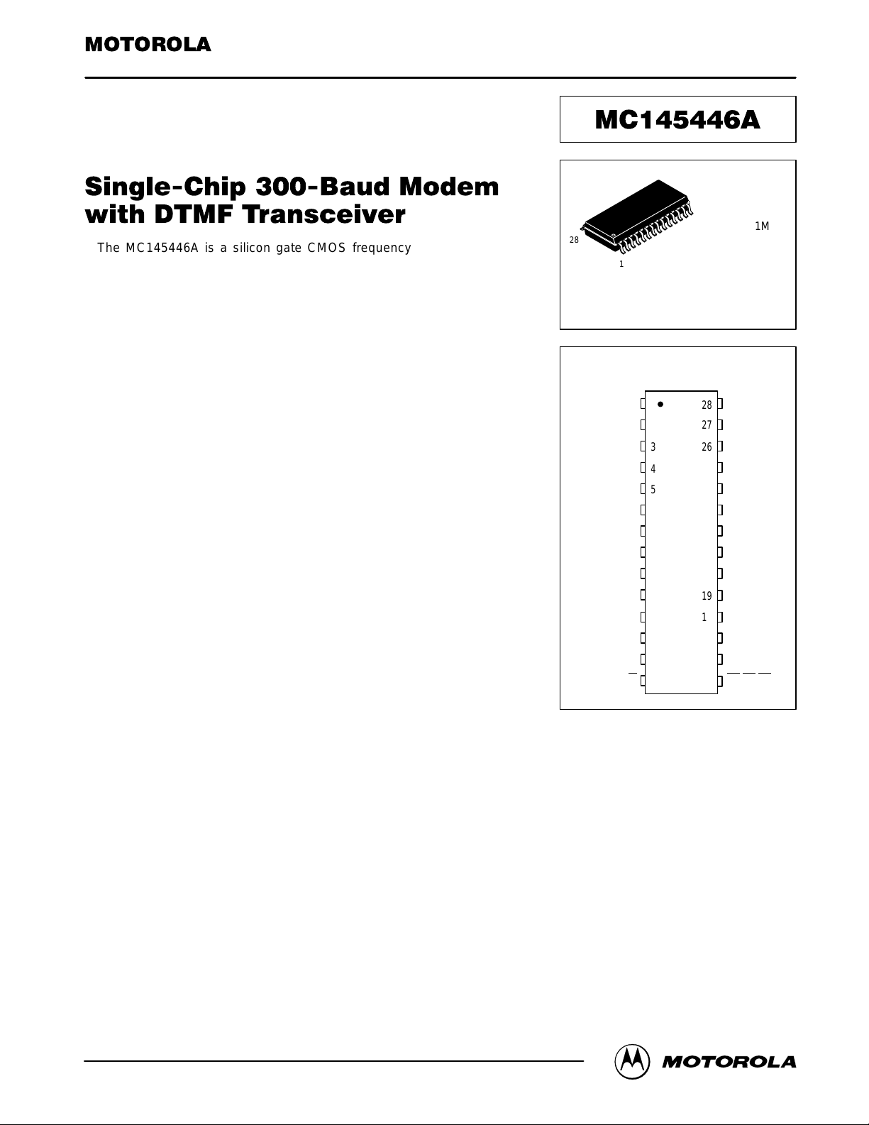
SEMICONDUCTOR TECHNICAL DATA
FW SUFFIX
SOP
CASE 751M
28
1
5
4
3
2
1
10
9
8
7
6
11
12
13
14
20
21
22
23
24
25
26
19
27
28
18
17
16
15
FTLC2
CDA
V
ref
GND
V
CC
TLA
FTLC3
DTMF IN
R/W
V
CC
GND
AGC OUT
X1
X2
TxA1
RxA
RxGC
RxBO
FTLC1
RxD
TxD
DATA I/O
SD
/CD/DV
E
DSI
TxA2
SCK
V
CC
PIN ASSIGNMENT
ORDERING INFORMATION
MC145446AFW SOP
Motorola, Inc. 1996
REV 1
7/96
Page 2
MC145446A MOTOROLA
2
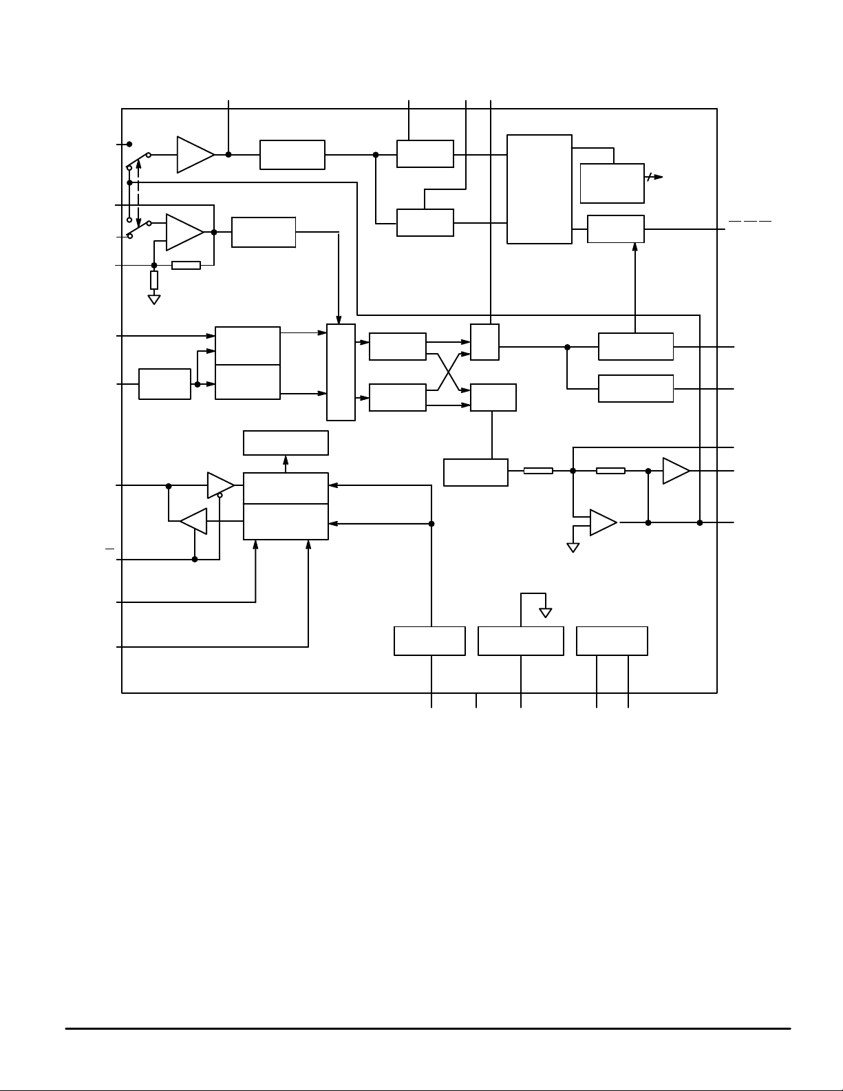
BLOCK DIAGRAM
MUX
CONTROL
SHIFT REGISTER
ANALOG GROUND
GENERATOR
+
+
_
SMOOTHING
FILTER
MUX
FSK
DEMODULATOR
FSK
MODULATOR
DTMF
GENERATOR
MODE CONTROL
LOGIC
STATUS
SHIFT REGISTER
POWER–ON
RESET
CLOCK
GENERATOR
NOISE
FILTER
LOW–BAND
BPF
HIGH–BAND
BPF
MUX/
MIXING
X1 X2V
ref
V
CC
GND
RxBO
DTMF
IN
RxGC
TxD
TLA
DATA
I/O
RxD
SD
/CD/DV
CDA
DSI
TxA1
TxA2
–
LOW–BAND
BPF
FREQUENCY
DETECTER
HIGH–BAND
BPF
CODE
CONVERTER
(DECODER)
TIMING
CIRCUIT
STATUS
REGISTER
SCK
RxA
E
R/W
4
AGC OUT FLTC2 FLTC3
FSK/DTMF LOOPBACK PATH
NOISE
FILTER
65 k
30 k
FLTC1
AGC
CARRIER/CPT
DETECTOR
– 1
LEVEL
CONTROL
Page 3
MC145446AMOTOROLA
3
ABSOLUTE MAXIMUM RATINGS (Voltages referenced to V
SS
)
Rating
Symbol Value Unit
DC Supply Voltage V
CC
– 0.5 to 7.0 V
DC Input Voltage V
in
– 0.5 to VCC + 0.5 V
DC Output Voltage V
out
– 0.5 to VCC + 0.5 V
Clamp Diode Current per Pin IIK, I
OK
± 20 mA
DC Current per Pin I
out
± 25 mA
Power Dissipation P
D
500 mW
Storage Temperature Range T
stg
– 65 to 150 °C
RECOMMENDED OPERATING CONDITIONS
Parameter Symbol Min Typ Max Unit
DC Supply Voltage V
CC
4.5 5 5.5 V
DC Input Voltage V
in
0 — V
CC
V
DC Output Voltage V
out
0 — V
CC
V
Input Rise Time t
r
0 — 500 ns
Input Fall Time t
f
0 — 500 ns
Crystal Frequency f
osc
— 3.579545 — MHz
Operating Temperature Range T
A
–20 25 70 °C
DC ELECTRICAL CHARACTERISTICS (V
CC
= 5.0 V ± 10%, TA = – 20 to 70°C)
Characteristic
Symbol Conditions Min Typ Max Unit
H Level V
IH
3.15 — — V
L Level V
IL
— — 1.1
H Level V
OH
IOH = 20 µA VCC – 0.1 VCC – 0.01 — V
L Level V
OL
IOL = 20 µA
IOL = 2 mA
—
—
0.01
—
0.1
0.4
Input Current TxD, E, SCK, DATA I/O, R/W I
in
Vin = VCC or GND — ± 1.0 ± 10.0 µA
I
CC
FSK Mode — 8 —
DCMF Receive Mode — 10 —
I
CC
Power–Down Mode 1 — — 500 µA
Power–Down Supply Current
Power–Down Mode 2 — — 1 µA
TRANSMIT CARRIER CHARACTERISTICS (V
CC
= 5.0 V ± 10%, TA = – 20 to 70°C)
Characteristic
Symbol Conditions Min Typ Max Unit
Mark ‘‘1’’ f
1M
974 980 986 Hz
Space ‘‘0’’ f
1S
3.579545 MHz
1174 1180 1186
Mark ‘‘1’’ f
2M
1644 1650 1656
Space ‘‘0’’ f
2S
1844 1850 1856
Answer Tone f
ans
2090 2100 2110
Transmit Carrier Level VO*
— 7 — dBm
Second Harmonic Energy V2h*
R
TLA
= ∞, RL = 1.2 kΩ,
V
– V
— – 46 — dBm
Out–of–Band Energy VOE*
V
TxA1
– V
TxA2
Figure 2 dBm
*V
TxA1
– V
TxA2
, RL = 1.2 kΩ
This device contains circuitry to protect the
inputs against damage due to high static voltages or electric fields; however, it is advised that
normal precautions be taken to avoid applications of any voltage higher than the maximum
rated voltages to this high impedance circuit.
For proper operation it is recommended that
Vin and V
out
be constrained to the range VSS ≤
(Vin or V
out
) ≤ VDD. Reliability of operation is
enhanced if unused inputs are tied to an
appropriate logic voltage level (e.g., either V
SS
or VDD).
Input Voltage
Output Voltage
Quiescent Supply Current
Carrier Frequency Channel 1
Carrier Frequency Channel 2
Crystal Frequency
Attenuator = 0 dB
mA
Page 4
MC145446A MOTOROLA
4
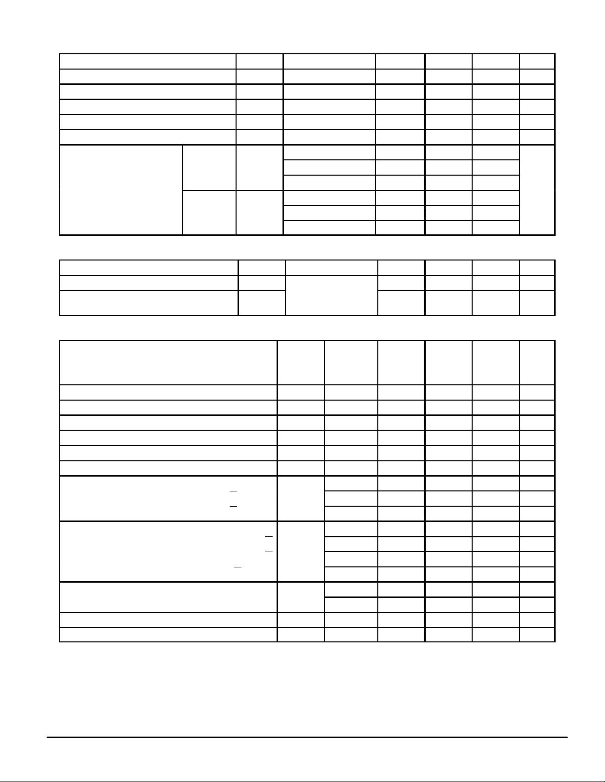
TRANSMIT ATTENUATOR CHARACTERISTICS (V
CC
= 5.0 V ± 10%, TA = – 20 to 70°C)
Characteristic
Symbol Conditions Min Typ Max Unit
Attenuator Range A
RNG
0 — 15 dB
1 dB – 5 dB
– 0.5 — 0.5
6 dB – 9 dB – 1 — 1
10 dB – 15 dB – 1.7 — 1
RECEIVER CHARACTERISTICS (INCLUDES HYBRID, DEMODULATOR, AND CARRIER DETECTOR)
(VCC = 5.0 V ± 10%, TA = – 20 to 70°C)
Characteristic
Symbol Conditions Min Typ Max Unit
Input Impedance R
IRX
RxA Pin 50 — — kΩ
Receiver Carrier Amplitude V
IRX
– 48 — – 12 dBm
Carrier Detect Threshold OFF to ON V
CDON
— – 44 — dBm
ON to OFF V
CDOF
fin = 1.0 kHz
— – 47 —
Hysterisis (V
CDON
– V
CDOF
) HYS 2 — — dB
CD1 = 0, CD0 = 0 — 450 — ms
CD1 = 0, CD0 = 1 — 10 —
CD1 = 1, CD0 = 0 — 10 —
CD1 = 1, CD0 = 1 — 70 —
CD1 = 0, CD0 = 0 — 35 —
CD1 = 0, CD0 = 1 — 35 —
CD1 = 1, CD0 = 0 — 20 —
CD1 = 1, CD0 = 1 — 15 —
CPTD CHARACTERISTICS (V
CC
= 5.0 V ± 10%, TA = – 20 to 70°C)
Characteristic
Symbol Conditions Min Typ Max Unit
Bandpass Filter Center Frequency f
c
— 400 — Hz
Bandpass Filter – 3 dB Band Width ∆
BW
— 140 — Hz
OFF to ON V
TDON
— – 44 — dBm
ON to OFF V
TDOF
fin = 400 Hz
— – 47 —
OFF to ON T
TDON
— 10 — ms
ON to OFF T
TDOF
— 25 —
DTMF TRANSMIT CHARACTERISTICS (V
CC
= 5.0 V ± 10%, TA = – 20 to 70°C)
Characteristic
Symbol Conditions Min Typ Max Unit
Low Group V
fl
— 2.5 — dBm
High Group V
fh
RTLA = ∞
Crystal Frequency
— 3.5 —
High Group Pre–Emphasis P
E
Crystal Frequency
3.579545 MHz
0 — 3 dB
DTMF Distortion DIST
Single Tone Mode
V
– V
,
— 5 — %
DTMF Frequency Variation ∆f
V
V
TxA1
– V
TxA2
,
RL = 1.2 kΩ
– 1 — 1 %
Out–of–Band Energy V
OE
Figure 1 dB
Setup Time t
osc
— 4 — ms
Attenuator Accuracy
A
ACC
Carrier Detect Timing OFF to ON T
ON to OFF T
CDON
CDOFF
CDA = 1.2 5V
dB
Tone Detect Level
Tone Detect Timing
Tone Output Level
CDA = 1.25 V
Attenuator = 0 dB
Page 5
MC145446AMOTOROLA
5
DTMF RECEIVER CHARACTERISTICS (V
CC
= 5.0 V ± 10%, TA = – 20 to 70°C)
Characteristic
Symbol Conditions Min Typ Max Unit
Input Impedance 50 — — kΩ
Detect Signal Level (Each Tone) – 48 — 0 dBm
Twist (High Group Tone/Low Group Tone – 10 — 10 dB
Frequency Detect Band Width (Figure 4) ±1.5% ±2Hz — — —
Frequency No–Detect Band Width (Figure 4) — — ± 3.5 %
CD1 = 0, CD0 = 1 — 25 —
CD1 = 1, CD0 = 0 — 30 —
CD1 = 1, CD0 = 1 — 40 —
CD1 = 0, CD0 = 1 — 25 —
CD1 = 1, CD0 = 0 — 35 —
CD1 = 1, CD0 = 1 — 25 —
DEMODULATOR CHARACTERISTICS (V
CC
= 5.0 V ± 10%, TA = – 20 to 70°C)
Characteristic
Symbol Conditions Min Typ Max Unit
Bit Bias ID
— 5 — %
Bit Error Rate
(CCITT Line Simulation, 511–Bit Pattern)
BER
S/N = 4 dB
— 0.00001 — —
SWITCHING CHARACTERISTICS (V
CC
= 5.0 V ± 10%, TA = – 20 to 70°C)
Characteristic
Symbol
Timing
Diagram
Reference
No.
Min Typ Max Unit
Input Pulse Width (H) E, SCK t
wh
1 50 — — ns
Input Pulse Width (L) E, SCK t
wl
2 50 — — ns
Clock Cycle t
c
3 100 — — ns
Input Rise Time t
r
4 — — 2 µs
Input Fall Time t
f
5 — — 2 µs
Recovery Time E to SCK t
rec
6, 18 50 — — ns
Setup Time DATA to SCK
7 50 — — ns
R/W↓ to DATA 9 100 — — ns
R/W↑ to DATA 12 50 — — ns
Hold Time SCK to DATA
8 50 — — ns
E to R/W 10 50 — — ns
DATA to R/W 14 50 — — ns
R/W to DATA 15 50 — — ns
Read Data Delay Time E to DATA
13 — — 50 ns
SCK to DATA 17 — — 50 ns
Enable Minimum Interval t
we
11 — — 450 ns
Mode Switch Minimum Interval t
wm
16 — — 600 ns
DTMF Detect Timing OFF to ON T
ON to OFF T
CDON
CDOFF
ms
Input Level = – 24 dBm
t
su
t
h
t
d
Page 6

MC145446A MOTOROLA
6
Figure 1. Serial Data Input Timing
CONTROL REGISTER
STATUS REGISTER
E*
(NOTE 6)
SCK
DATA
R/W
(LSB CLOCK)
*The enable signal corresponds to preceding data format.
CH SQ T3 T2 T1 T0 A3 A2 A1 A0 M3 M2 M1 M0CD1 CD0
E
SCK
DATA
R/W
1 2 3
NOTES:
1. The data in front of the enable signal pulse will be latched.
2. The latched data will be repeated until there is an enable pulse.
3. The detected data will be updated with the next enable pulse.
4. After the R/W
pin becomes INACTIVE, the data will be lost.
5. D1 corresponds to Clock1.
6. The enable and the SCK signals need to be set at the logic low level when the R/W
signal changes.
7. The SCK must be held at low level when the enable signal is at high level.
(NOTE 4)
(NOTE 5)
(NOTE 2)
(NOTE 3)
(NOTE 1)
5 6 7 8 9 10 11 12 13 144 15 16
2
3
4
5
16
1
2
3
4
5
6
7
8
9
10
11
12
13
7
1
1
2
D2D0 D1 D1D0 D1D0D3 D2
3 0 1 2 1
1 2
(HIGH–IMPEDANCE)
17
18
4
5
14
15
1
(NOTE 7)
Page 7

MC145446AMOTOROLA
7
Figure 2. Out–of–Band Energy
– 55
– 15 dB/OCT.
f (Hz)
256 k16 k4 k3.4 k0
0
– 25
TRANSMIT CARRIER LEVEL (dBr)
Figure 3. FSK, DTMF Carrier Detect Timing
V
on
V
off
RxA, DTMF IN
SD/DV/CD
t
off
t
on
Figure 4. DTMF Frequency Detect Bandwidth
NO–DETECT
DETECT MINIMUM
WIDTH
NO–DETECT
– 3.5%
– 1.5% – 2 Hz + 1.5% + 2 Hz
+ 3.5%
f
o
Page 8

MC145446A MOTOROLA
8
PIN DESCRIPTIONS
V
CC
Positive Power Supply (Pins 1, 13, 21)
The digital supply pins, which are connected to the positive
power supply (5 V).
GND
Ground Pins (Pins 2, 12)
The ground pins are connected to the system ground.
V
ref
Reference Analog Ground (Pin 3)
This pin provides the analog ground voltage, which is internally regulated to VCC/2. It should be decoupled to the GND
with 0.1 µF and 100 µF capacitors.
X1
Crystal Oscillator Output (Pin 9)
A 3.579545 MHz ± 0.1% crystal oscillator is tied to this pin
with the other end connected to X2.
X2
Crystal Oscillator Input (Pin 10)
A 3.579545 MHz ± 0.1% crystal oscillator is tied to this pin
with the other end connected to X1. X2 may also be driven
directly from an appropriate external source.
SCK
Serial Clock Input (Pin 19)
This pin is the clock input for the 16–bit control resistor and
the 4–bit status resistor. The serial data is captured into the
control register, or is shifted out of the status register on the
rising edge of SCK.
DATA I/O
Serial Data Input/Output (Pin 18)
This pin is the 16–bit control register input, which determines the operation mode, DTMF tone, transmit attenuation
(receiver gain), carrier detect time, channel, and transmit
squelch. This pin is also the four–bit status register output
which indicates the received DTMF t one (hexadecimal
codes).
E
Enable Input (Pin 20)
When the R/W
pin is at logic low, high level on the E pin
makes the 16–bit control register data transparent to the
mode control logic so that the device operation is changed.
While this pin is at logic low, the control register and the
mode control logic are isolated. The E pin must NOT be held
high while the control register data is being changed.
When the R/W
pin is at logic high, the rising edge of E
transfers the four–bit DTMF data from the DTMF decoder to
the status register. Then the first bit (LSB = D0) is presented
at the Data I/O pin.
R/W
Read/Write Data Switch (Pin 14)
This pin is used for controlling the I/O direction of the Data
I/O pin.
TxD
Transmit Data Input (Pin 17)
This pin is the transmit data input. When the device is in
FSK mode, the mark frequency is generated when this pin is
at the logic high level. The space frequency is generated
when the pin is at a logic low.
RxD
Receive Data Output (Pin 16)
This pin is the receive data output. When the device is in
the FSK mode, a high logic level of this pin indicates that the
mark carrier frequency has been received, and a low logic
level indicates the space carrier frequency has been received.
SD
/CD/DV
Carrier/Call Progress Tone Detect/DTMF Data Valid
Detect (Pin 15)
This pin works as a carrier detector in the FSK mode,
whereas it works as the call progress tone detector in the
CPTD mode and as the receive DTMF detector in the DTMF
Rx mode. The output goes to a logic low level when the input
signal reaches the minimum threshold of the detect level that
is adjusted by the CDA voltage. When this pin is logic high,
the receive data output (RxD) is clamped high to avoid the
error that may occur with the loop noise.
In DTMF Rx mode, the logic low on this pin indicates that
the valid DTMF frequencies are detected. The received tone
is decoded to four–bit data, then stored in the DTMF decoder
by the falling edge of DV
.
TxA1
Non–Inverting Transmit Analog Carrier Output (Pin 24)
This pin is the line driver non–inverting output. A 7 dBm
(typ) differential output voltage can be obtained by connecting a 1.2 kΩ load resistor between Tx1 and Tx2. Attention
must be paid so as not to exceed this level when an external
input is added to the DSI pin. A telephone line (600 Ω) is driven through an external 600 Ω resistor (see the Application
Circuit). In this case, the output level becomes about a half of
the differential output.
TxA2
Inverting Transmit Analog Carrier Output (Pin 23)
This pin is the line driver inverting output. The signal is
equal in magnitude, but 180° out of phase with the T xA1
(refer to TxA1).
RxA
Receive Signal Input (Pin 25)
This pin is the carrier signal input, and is enabled when the
device is in FSK or CPTD mode.
RxGC
Receive Gain Adjust (Pin 26)
This pin is used to adjust the receive buffer gain. To adjust
the gain, a resistor may be added between this pin and the
RxBO pin (refer to the Block Diagram). This pin may be held
open when the gain adjustment is not needed.
RxBO
Receive Buffer Output (Pin 27)
This pin is the receive buffer output.
Page 9

MC145446AMOTOROLA
9
DTMF IN
DTMF Receive Input (AGC Amp Input) (Pin 5)
This pin is the receive DTMF signal input. It is enabled
when the device is in the DTMF receive mode.
AGC OUT
AGC Output (Pin 6)
This pin is used by the manufacturer to test the auto gain
control amplifier. It should be held open in normal operation.
DSI
Driver Summing Input (Pin 22)
This pin is the inverting input of the line driver. An external
signal may be transmitted through an external series resistor
R
DSI
. The differential gain G
DSI
= (V
TxA1
– V
TxA2
)/V
DSI
is determined by the following equation:
G
DSI
= – 2Rf / R
DSI
, Rf X 20 kΩ
Note that the programmable transmit attenuator does not
affect in this case.
The DSI pin should be held open when not in use.
CDA
Carrier Detect Level/CPTD Level Control (Pin 4)
The carrier/call progress tone detect level is adjusted by
the CDA pin voltage.
When this pin is held open, the CDA voltage i s set to
1.25 V (VCC = ± 5 V) by an internal divider. Then the detect
level is set at – 44 dBm (typ) for off to on, and – 47 dBm (typ)
for on to off, and the hysteresis is set minimum 2 dB. This pin
has a very high input impedance so it should be connected to
GND with a 0.1 µF capacitor to keep it under the regulations.
An external voltage may be applied to this pin to adjust the
carrier detect threshold. The following equations may be
used to find the CDA voltage required for a given threshold
voltage:
V
CDA
= 245 × V
on
V
CDA
= 347 × V
off
TLA
Transmit Carrier Level Adjust (Pin 11)
This pin is used to adjust the transmit carrier level that is
determined by the value of the resistor (RTLA) connected
between this pin and the GND. The maximum level can be
obtained when this pin is shorted to GND (RTLA = 0).
FTLC1
FSK Filter Test (Pin 28)
This pin is a high–impedence filter output. It may be used
for testing the FSK filter characteristics, and is reserved for
manufacturer’s use only. In normal operation, this pin should
be decoupled to V
ref
with a 0.1 µF capacitor.
FTLC2
DTMF Receive Low Group Filter Test (Pin 7)
This pin is a high–impedence filter output. It may be used
for testing the DTMF receive high goup bandpass filter characteristics, and is reserved for manufacturer’s use only. In
normal operation, this pin should be decoupled to V
ref
with a
0.1 µF capacitor.
FTLC3
DTMF Receive High Group Filter Test (Pin 8)
This pin is a high–impedence filter output. It may be used
for testing the DTMF receive high group bandpass filter characteristics, and is reserved for manufacturer’s use only. In
normal operation, this pin should be decoupled to V
ref
with a
0.1 µF capacitor.
SERIAL CONTROL INTERFACE
The following six functions are determined by the 16 bits of
serial data in the control register.
T3 T2 T1 T0
CD1 CD0
A2
A1 A0
TRANSMIT TONE
FREQUENCY :
CARRIER DETECT TIME :
CHANNEL :
SQTRANSMIT SQUELCH :
FUNCTION MODE :
TRANSMIT ATTENUATOR :CHA3
CONTROL REGISTER
M2 M1 M0
M3
The received DTMF tones are indicated by the four bits of
data in the status register.
D3 D2 D1 D0RECEIVE TONE FREQUENCY:
STATUS REGISTER
Figure 1 presents the timing diagram of 16–bit control register input and four–bit status output. When the R/W
pin is in
logic low, the 16–bit data is captured into the control register
at the rising edge of SCK and latched in the mode control
logic to update the function mode at logic high input to the E
pin. When the R/W
pin is in logic high, the status register is
selected to read out the received DTMF data, the four–bit
data in the DTMF decoder is loaded into the status register,
and the first bit (D0) is presented at the Data I/O on the rising
edge of E. The following bits are repeatedly shifted out as
D1–D2–D3–D0–D1–... by the rising edges of SCK.
CONTROL REGISTER BIT MAP DESCRIPTION
FUNCTION MODE (M3 to M0)
One of the following modes is selected from the four–bit
data (M3 to M0) shown in Table 1. Table 2 presents each output status; the functions are described below.
Page 10

MC145446A MOTOROLA
10
Table 1. Function Mode Truth Table
M3 M2 M1 M0 Function Mode
0 0 0 0 FSK
0 0 0 1 FSK Analog Loopback
0 0 1 0 CPTD
0 0 1 1 Answer Tone
0 1 0 0 DTMF Transmit
0 1 0 1 Single Tone
0 1 1 0 Power–Down 1
0 1 1 1 Power–Down 2
1 0 0 0 DTMF Receive
1 0 0 1 DTMF Analog Loopback
FSK Mode
The transmitter and t he receiver work as a n FSK modu-
lator/demodulator. The SD
pin goes low when a valid F SK
signal is detected.
DTMF Transmit Mode
The transmitter works as a DTMF tone generator. The
receiver is disabled.
CPTD (Call Progress Tone Detect) Mode
The receiver works as a 400 Hz call progress tone detec-
tor. The CD
pin goes low when a valid call progress tone is
detected.
Answer Tone Mode
The transmitter works as a 2100 Hz answer tone genera-
tor. The receiver is disabled.
FSK Analog Loopback Mode
The transmitter, working as the FSK modulator, is internally connected to the receiver working as the FSK demodulator. This feature is used for the device self test.
DTMF Receive Mode
The receiver works as a DTMF tone receiver . The DV
goes
low when a valid DTMF tone is detected. The transmitter is
disabled.
DTMF Analog Loopback Mode
The transmitter, working as a DTMF tone generator, is internally connected to the receiver working as DTMF tone receiver. The DV
goes low when the receiver detects a valid
DTMF tone. This feature is used for the device self test.
Single Tone Mode
The transmitter generates one of the eight frequencies of
the DTMF tone. The receiver is disabled.
Power–Down Mode 1
Whole internal circuits, except the oscillator, are disabled
and all outputs except the X1 pin go to the high–impedance
state. The supply current decreases to 500 µA (max).
Power–Down Mode 2
Whole internal circuits, including the oscillator, are disabled and all outputs go to the high–impedance state. The
supply current decreases to 1.0 µA (max).
Transmit Attenuator/AGC Gain Set (A3 to A0)
Four–bit serial data (A3 – A0) sets up the analog transmit
level in the FSK, answer tone, DTMF, analog loopback, and
single tone mode. The range of the transmit attenuator is 0 to
15 dB in 1 dB steps. The attenuator, however, does not affect
the external signal input from the DSI. These bits also determine the AGC amplifier gain in the DTMF receive mode. In
normal operation, “Automatic” may be selected so that the
gain is automatically adjusted corresponding to the input signal level. See Table 3 for a detailed description.
Transmit Tone Frequency (T3 to T0)
These four bits (T3 to T0) determine the DTMF tone frequencies in DTMF transmit and DTMF analog loopback
mode, and determine the single tone frequency in the single
tone mode. Tone frequency assignments with reference to
T3 – T0 are shown in Table 4.
Table 2. Output Status
Output Pin
Function Mode
RxD SD/CD/DV TxA1, TxA2
FSK
FSK
FSK Loopback
Digital Data
Detect Signal
Call Progress Tone H CPTD Signal VCC/2
Answer Tone H H Answer Tone
DTMF Transmit H H DTMF Tone
Single Tone H H Single Tone
Power–Down 1, 2 High Impedance High Impedance High Impedance
DTMF Receive
VCC/2
DTMF Loopback DTMF Tone
Receive
H DV Signal
Carrier
Page 11

MC145446AMOTOROLA
11
Table 3. Transmit Attenuator/AGC Gain Set
Truth Table
A3 A2 A1 A0
Attenuation
(dB)
AGC Gain
Step (dB)
0 0 0 0 0 – 5.0
0 0 0 1 1 – 2.5
0 0 1 0 2 0.0
0 0 1 1 3 2.5
0 1 0 0 4 5.0
0 1 0 1 5 7.5
0 1 1 0 6 10.0
0 1 1 1 7 12.5
1 0 0 0 8 15.0
1 0 0 1 9 17.5
1 0 1 0 10 20.0
1 0 1 1 11 Clamp
1 1 0 0 12 Automatic
1 1 0 1 13 —
1 1 1 0 14 —
1 1 1 1 15 —
Table 4. Tone Frequency Truth Table
Tone Frequency (Hz)
DTMF Mode
T3/D3
T2/D2
T1/D1
T0/D0
Low
Group
High
Group
Keyboard
Equivalent
Single
Tone Mode
0 0 0 0 941 1633 D 941
0 0 0 1 697 1209 1 697
0 0 1 0 697 1336 2 697
0 0 1 1 697 1477 3 697
0 1 0 0 770 1209 4 770
0 1 0 1 770 1336 5 770
0 1 1 0 770 1477 6 770
0 1 1 1 852 1209 7 852
1 0 0 0 852 1336 8 1336
1 0 0 1 852 1477 9 1477
1 0 1 0 941 1336 0 1336
1 0 1 1 941 1209 * 1209
1 1 0 0 941 1477 # 1477
1 1 0 1 697 1633 A 1633
1 1 1 0 770 1633 B 1633
1 1 1 1 852 1633 C 1633
Page 12

MC145446A MOTOROLA
12
Transmit Squelch
The 1–bit serial data (SQ) controls the transmit analog
squelch. The FSK signal, DTMF tones, single tone, and answer tone are disabled, then TxA1 and TxA2 will be clamped
to VCC/2 when the transmit squelch goes to the Enable (SQ
= 1) state. The transmit squelch does not affect the external
signal from the DSI.
Table 5. Transmit Squelch Truth Table
SQ Squelch
1 Enable
0 Disable
Channel
When the function mode is either on the FSK or analog
loopback mode, the transmit and receive channel is set up
with a 1–bit serial data (CH).
Table 6. Channel Truth Table
CH Channel
1 1 (Originate)
0 2 (Answer)
Carrier Detect Time
The carrier and DTMF tone detect timing are determined
by two–bit serial d ata (CD1, CD0). The timing diagram is
shown in Figure 3.
Table 7. Carrier/DTMF Detect Time Truth Table
FSK Mode
Carrier Detect Time
(typ)
DTMF Receive Mode
Carrier Detect Time
(typ)
CD1
CD0
ton (ms) t
off
(ms) ton (ms) t
off
(ms)
0 0 450 35 Reserved
0 1 10 35 25 25
1 0 10 20 30 35
1 1 70 15 40 25
Power–On Reset
When the power is switched on, this device is entered into
Power–Down Mode 2 by the internal power–on reset circuit.
STATUS REGISTER BIT MAP DESCRIPTION
Received Tone Frequency (D3 to D0)
This four–bit data (D3 to D0) indicates the received DTMF
tones. The first bit (D0) is presented at Data I/O on the rising
edge of E, and the following bits (D1–D2–D3–D0–D1– ...)
are shifted out and presented on the next rising edge of SCK.
The d ata configuration c orresponding t o each tone is
shown in Table 4.
Page 13

MC145446AMOTOROLA
13
100 µF 0.1 µF
V
REF
FTLC1
CDA
0.1 µF
0.1
µ
F
0.1
µ
F
TLA
DSI
TxA2
TxA1
DTMF IN
RxGC
RxBO
TxD
RxD
SD/CD/DV
DATA I/O
SCK
E
0.1 µF
V
CC
+ 5 V
600 : 600
10
Ω
600
Ω
TIP
RING
GND
MCU
I/O PORT
LINE PROTECTION CIRCUIT REFERENCE ANALOG GROUNDSYSTEM GROUND
*
*
Figure 5. Application Circuit
MC145446A
R/W
RxA
FTLC3
0.1 µF
FTLC2
0.1 µF
100 µF
Page 14

MC145446A MOTOROLA
14
PACKAGE DIMENSIONS
FW SUFFIX
SOP
CASE 751M–01
NOTES:
1. DIMENSIONING AND TOLERANCING PER ANSI
Y14.5M, 1982.
2. CONTROLLING DIMENSION: MILLIMETER.
3. DIMENSIONS A AND B DO NOT INCLUDE MOLD
PROTRUSION. MAXIMUM MOLD PROTRUSION
SHALL NOT EXCEED 0.15 (0.006) PER SIDE.
4. DIMENSION D DOES NOT INCLUDE DAMBAR
PROTRUSION. DAMBAR PROTRUSION SHALL
NOT CAUSE THE LEAD WIDTH TO EXCEED 0.65
(0.026).
DIMAMIN MAX MIN MAX
INCHES
17.80 18.03 0.701 0.710
MILLIMETERS
B 7.40 7.62 0.291 0.300
C 2.65 0.104
C1 2.25 2.45 0.090 0.096
D 0.35 0.51 0.014 0.020
E 10.00 10.60 0.394 0.414
F 0.40 0.70 0.016 0.028
G 1.27 BSC 0.050 BSC
J 0.10 0.25 0.004 0.010
L 0.635 BSC 0.025 BSC
θ
8 8
V 0.25 0.75 0.010 0.030
W 0.05 0.20 0.002 0.008
X 1.40 REF 0.110 REF
C
L
_ _
Y0.25 (0.010)MT Z
S S
-Y-
A
-Z-
B
1 14
1528
D 28X
Z0.18 (0.007)MT Y
S S
0.18 (0.007)MT
0.10 (0.004) T
E
VIEW AB
V X 45
_ " 5_
C
W
-T-
L
4X
G 24X
SEATING
PLANE
θ
J
F
Z
C1
W REF
VIEW AB
Motorola reserves the right to make changes without further notice to any products herein. Motorola makes no warranty , representation or guarantee regarding
the suitability of its products for any particular purpose, nor does Motorola assume any liability arising out of the application or use of any product or circuit, and
specifically disclaims any and all liability , including without limitation consequential or incidental damages. “Typical” parameters which may be provided in Motorola
data sheets and/or specifications can and do vary in different applications and actual performance may vary over time. All operating parameters, including “Typicals”
must be validated for each customer application by customer’s technical experts. Motorola does not convey any license under its patent rights nor the rights of
others. Motorola products are not designed, intended, or authorized for use as components in systems intended for surgical implant into the body, or other
applications intended to support or sustain life, or for any other application in which the failure of the Motorola product could create a situation where personal injury
or death may occur. Should Buyer purchase or use Motorola products for any such unintended or unauthorized application, Buyer shall indemnify and hold Motorola
and its officers, employees, subsidiaries, affiliates, and distributors harmless against all claims, costs, damages, and expenses, and reasonable attorney fees
arising out of, directly or indirectly, any claim of personal injury or death associated with such unintended or unauthorized use, even if such claim alleges that
Motorola was negligent regarding the design or manufacture of the part. Motorola and are registered trademarks of Motorola, Inc. Motorola, Inc. is an Equal
Opportunity/Affirmative Action Employer.
How to reach us:
USA/EUROPE/Locations Not Listed: Motorola Literature Distribution; JAPAN: Nippon Motorola Ltd.; Tatsumi–SPD–JLDC, 6F Seibu–Butsuryu–Center,
P.O. Box 20912; Phoenix, Arizona 85036. 1–800–441–2447 or 602–303–5454 3–14–2 Tatsumi Koto–Ku, Tokyo 135, Japan. 03–81–3521–8315
MFAX: RMFAX0@email.sps.mot.com – TOUCHTONE 602–244–6609 ASIA/PACIFIC: Motorola Semiconductors H.K. Ltd.; 8B Tai Ping Industrial Park,
INTERNET: http://Design–NET.com 51 Ting Kok Road, Tai Po, N.T., Hong Kong. 852–26629298
MC145446A/D
*MC145446A/D*
◊
 Loading...