

Page 1
MC145444MOTOROLA
1
Advance Information
MC145444 is a silicon gate CMOS frequency shift keying (FSK) modem
intended for use with telemeter systems or remote control systems over the
telephone network.
This device is compatible with CCITT V .21 and contains the entire circuit that
provides a full–duplex or half–duplex 300–baud data communication over a pair
of telephone lines. This device also includes the DTMF generator and call
progress tone detector (CPTD).
The differential line driver has the capability of driving 0 dBm into a 600 Ω load
with a single +5 V power supply.
The transmit level is controlled by the programmable attenuator in 1 dB steps.
Devices functions are controlled through a 3–wire serial interface.
• Capable of Driving 0 dBm into a 600 Ω Load
• DTMF Generator On–Chip
• Imprecise Call Progress Detector On–Chip
• A Transmit Attenuator Programmable in 1 dB Steps
• 3–Wire Serial Interface
• Compatible with CCITT V.21
• 2100 Hz Answer Tone Generator On–Chip
• Analog Loopback Configuration for Self Test
• Simplex, Half–Duplex, and Full–Duplex Operation
This document contains information on a new product. Specifications and information herein are subject to change without notice.
Order this document
by MC145444/D
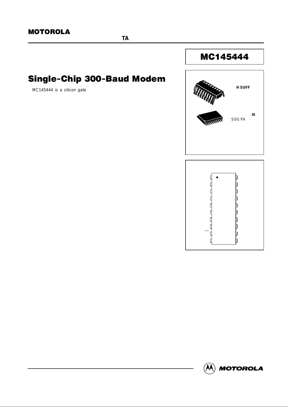
SEMICONDUCTOR TECHNICAL DATA
H SUFFIX
PLASTIC DIP
CASE 804
DW SUFFIX
SOG PACKAGE
CASE 751D
20
1
20
1
TLA
CDA
GNDA
FTLC
RxBO
RxD
SD
X2
X1
GND 5
4
3
2
1
10
9
8
7
6
14
15
16
17
18
19
20
11
12
13
DSI
TxA2
TxA1
RxA
RxGC
TxD
DATA
SCK
ENB
V
CC
PIN ASSIGNMENT
ORDERING INFORMATION
MC145444P Plastic DIP
MC145444DW SOG Package
Motorola, Inc. 1995
REV 0
8/95
Page 2
MC145444 MOTOROLA
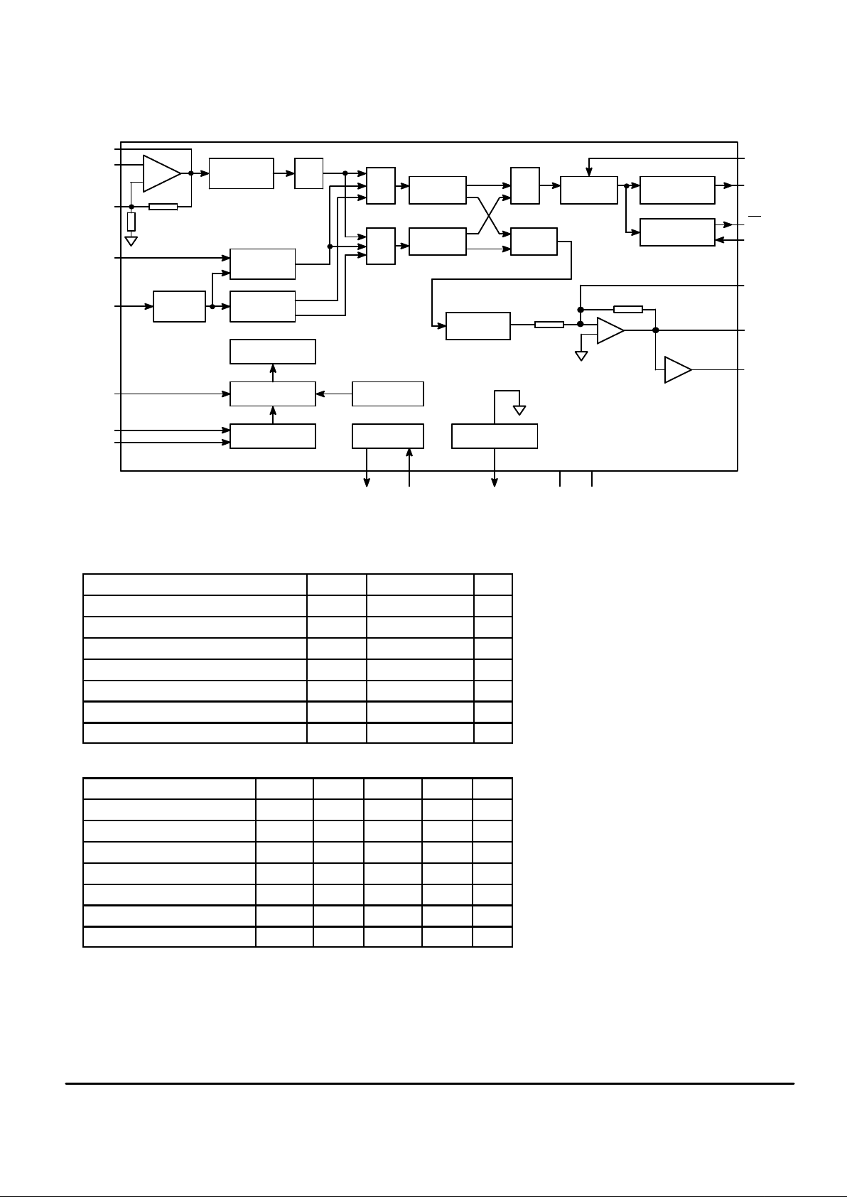
2
MUX
15–BIT
LATCH
ANALOG GROUND
GENERAT OR
BLOCK DIAGRAM
+
+
_
– 1
FSK
DEMODULATOR
SMOOTHING
FILTER
MUX
CARRIER/CPT
DETECTOR
FSK
MODULA TOR
DTMF
GENERATOR
LEVEL
CONTROL
CONTROL
LOGIC
15–BIT
SHIFT REGISTER
POWER–ON
RESET
CLOCK
GENERAT OR
ANTI–ALIAS
FILTER
LOW–BAND
BPF
HIGH–BAND
BPF
MUX/
MIXING
AC AMP
MUX
S/H
Rf
R
FTLC
X1 X2 GND V
CC
GNDA
RxBO
RxA
RxGC
TxD
TLA
ENB
DATA
SCK
RxD
SD
CDA
DSI
TxA1
TxA2
–
65 k
20 k
30 k
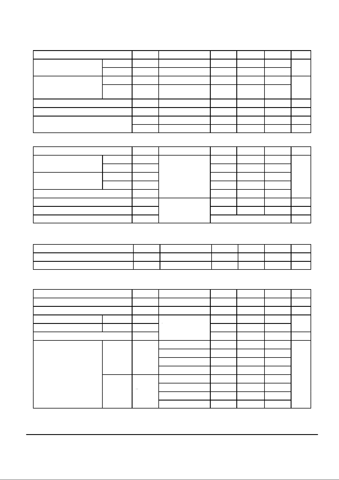
MAXIMUM RATINGS* (Voltages Referenced to V
SS
)
Rating
Symbol Value Unit
DC Supply Voltage V
CC
– 0.5 to + 7.0 V
DC Input Voltage V
in
– 0.5 to VCC + 0.5 V
DC Output Voltage V
out
– 0.5 to VCC + 0.5 V
Clamp Diode Current per Pin IIK, I
OK
± 20 mA
DC Current per Pin I
out
± 25 mA
Power Dissipation P
D
500 mW
Storage Temperature Range T
stg
– 65 to + 150 °C
RECOMMENDED OPERATING CONDITIONS
Parameter Symbol Min Typ Max Unit
DC Supply Voltage V
CC
4.5 5 5.5 V
DC Input Voltage V
in
0 — V
CC
V
DC Output Voltage V
out
0 — V
CC
V
Input Rise Time t
r
0 — 500 ns
Input Fall Time t
f
0 — 500 ns
Crystal Frequency f
osc
— 3.579545 — MHz
Operating Temperature Range T
A
– 20 25 70 °C
Page 3
MC145444MOTOROLA
3
DC ELECTRICAL CHARACTERISTICS (V
CC
= + 5.0 V ± 10%, TA = – 20 to + 70°C)
Characteristic Symbol Conditions Min Typ Max Unit
Input Voltage
H Level V
IH
3.15 — — V
L Level V
IL
— — 1.1
Output Voltage
H Level V
OH
IOH = 20 µA VCC – 0.1 VCC – 0.01 — V
L Level V
OL
IOL = 20 µA
IOL = 2 mA
—
—
0.01
—
0.1
0.4
Input Current DATA, SCK, E, TxD I
in
Vin = VCC or GND — ± 1.0 ± 10.0 µA
Quiescent Supply Current I
CC
FSK Mode — 8 — mA
–
I
CC
Power–Down Mode 1 — — 300 µA
Power–Down Supply Current
I
CC
Power–Down Mode 2 — — 1 µA
TRANSMIT CARRIER CHARACTERISTICS (V
CC
= + 5.0 V ± 10%, TA = – 20 to + 70°C)
Characteristic
Symbol Conditions Min Typ Max Unit
Carrier Frequency Channel 1
Mark ‘‘1’’ f
1M
974 980 986 Hz
Space ‘‘0’’ f
1S
1174 1180 1186
Carrier Frequency Channel 2
Mark ‘‘1’’ f
2M
Crystal Frequency
3.579545 MHz
1644 1650 1656
Space ‘‘0’’ f
2S
3.579545 MHz
1844 1850 1856
Answer Tone f
ans
2094 2100 2106
Transmit Carrier Level VO*
— 6 — dBm
Second Harmonic Energy V2h*
Attenuator = 0 dB
RTLA = ∞
— – 46 — dBm
Out–of–Band Energy VOE*
RTLA = ∞
Figure 1 dBm
*V
TXA1
– V
TXA2
, RL = 1.2 kΩ
TRANSMIT ATTENUATOR CHARACTERISTICS (V
CC
= + 5.0 V ± 10%, TA = – 20 to + 70°C)
Characteristic Symbol Conditions Min Typ Max Unit
Attenuator Range A
RNG
0 — 15 dB
Attenuator Accuracy A
ACC
– 0.5 — + 0.5 dB
RECEIVER CHARACTERISTICS (Includes Hybrid, Demodulator and Carrier Detector)
(VCC = + 5.0 V ± 10%, TA = – 20 to + 70°C)
Characteristic
Symbol Conditions Min Typ Max Unit
Input Impedance R
IRX
RxA Pin (Pin 19) 50 — — kΩ
Receiver Carrier Amplitude V
IRX
– 48 — – 12 dBm
Carrier Detect OFF to ON V
CDON
CDA = 1.2 V
— – 44 — dBm
Threshold ON to OFF V
CDOF
fin = 1.0 kHz
— – 47 —
Hysterisis (V
CDON
– V
CCDOF
) H
VS
2 — — dB
Carrier Detect Timing OFF to ON
CD1 = 0, CD0 = 0 — 450 — ms
CD1 = 0, CD0 = 1 — 15 —
T
CDON
CD1 = 0, CD1 = 1 — 15 —
CD1 = 1, CD0 = 1 — 80 —
ON to OFF
CD1 = 0, CD0 = 0 — 30 —
CD1 = 0, CD0 = 1 — 30 —
T
CDOFF
CD1 = 0, CD0 = 1 — 15 —
CD1 = 1, CD0 = 1 — 10 —
Page 4
MC145444 MOTOROLA
4
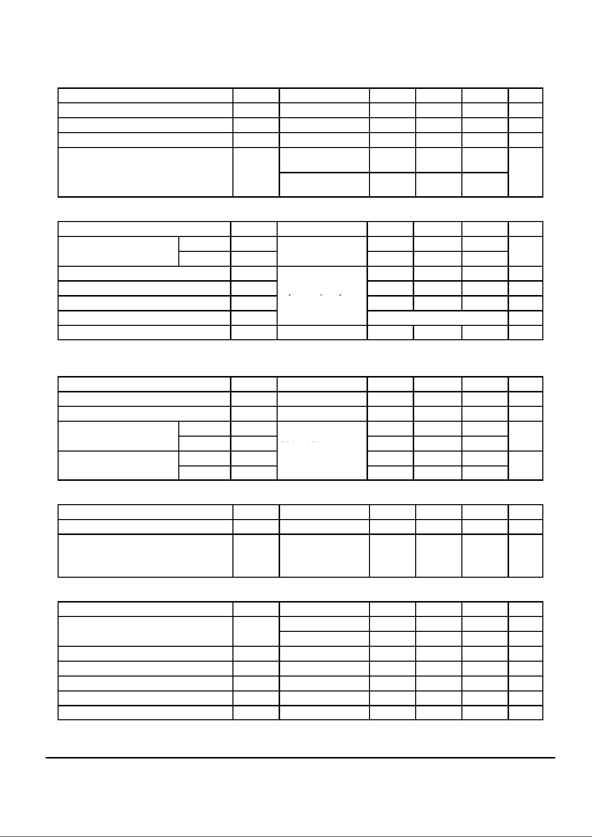
BAND–PASS FILTER CHARACTERISTICS (RxA to FTLC) (V
CC
= + 5.0 V ± 10%, TA = – 20 to + 70°C)
Characteristic Symbol Conditions Min Typ Max Unit
FTLC Output Impedance R
OFT
10 — 50 kΩ
Adjacent Channel Rejection REJ V
RXA
= – 12 dBm — 50 — dB
Pass–Band Gain G
PAS
— 10 — dB
Group Delay
Low–Band Filter
930 – 1230 Hz
— 700 —
µs
High–Band Filter
1600 – 1900 Hz
— 800 —
DTMF CHARACTERISTICS (V
CC
= + 5.0 V ± 10%, TA = – 20 to + 70°C)
Characteristic Symbol Conditions Min Typ Max Unit
Tone Output Level
Low Group Vfl* — 3 — dBm
High Group Vfh*
— 4 —
High Group Pre Emphasis P
E
Attenuator = 0 dB
0 — 3 dB
DTMF Distortion DIST
RTLA = ∞
Crystal Frequency
— 5 — %
DTMF Frequency Variation ∆f
V
Crystal Frequency
3.579545 MHz
– 1 — 1 %
Out–of–Band Energy VOE* Figure 1 dB
Setup Time t
osc
— 4 — ms
*V
TXA1
– V
TXA2
, RL = 1.2 kΩ
CPTD CHARACTERISTICS (V
CC
= + 5.0 V ± 10%, TA = – 20 to + 70°C)
Characteristic
Symbol Conditions Min Typ Max Unit
Band–Pass Filter Center Frequency f
c
— 400 — Hz
Band–Pass Filter – 3 dB Band Width ∆
BW
— 140 — Hz
Tone Detect Level
OFF to ON V
TDON
— – 44 — dBm
ON to OFF V
TDOF
CDA = 1.2 V
— – 47 —
Tone Detect Timing
OFF to ON T
TDON
fin = 400 Hz
— 10 — ms
ON to OFF T
TDOF
— 25 —
DEMODULATOR CHARACTERISTICS (V
CC
= + 5.0 V ± 10%, TA = – 20 to + 70°C)
Characteristic Symbol Conditions Min Typ Max Unit
Bit Bias ID Input Level = – 24 dBm — 5 — %
Bit Error Rate BER Input Level = – 24 dBm
CCITT Line Simulation
511 Bit Pattern
S/N = 5 dB
— 0.00001 — —
SWITCHING CHARACTERISTICS (V
CC
= + 5.0 V ± 10%, TA = – 20 to + 70°C)
Characteristic Symbol Conditions Min Typ Max Unit
Setup Times DATA to SCK t
su
50 — — ns
SCK to ENB 50 — — ns
Hold Time SCK to DATA t
h
50 — — ns
Recovery Time ENB to SCK t
rec
50 — — ns
Input Rise Time t
r
— — 2 µs
Input Fall Time t
f
— — 2 µs
Input Pulse Width ENB, SCK t
w
50 — — ns
Page 5

MC145444MOTOROLA
5
Figure 1. Out–of–Band Energy Figure 2. Switching Characteristics
– 55
– 15 dB/OCT.
f (Hz)
256 k16 k4 k3.4 k0
0
– 25
50%
50%
DATA
SCK
ENB
ENB
50%
50%
50%
PREVIOUS
DATA LATCHED
LAST
CLK
FIRST
CLK
t
su
t
h
t
r
t
f
t
su
t
rec
— V
CC
— GND
— V
CC
— GND
— V
CC
— GND
— V
CC
— GND
PIN DESCRIPTION
V
CC
Positive Power Supply (Pin 15)
This pin is normally tied to the + 5.0 V . A 0.1 µF decoupling
capacitor should be used.
GND
Ground Pin (Pin 5)
This pin is normally tied to 0 V.
GNDA
Analog Ground (Pin 3)
Analog ground is internally biased to (VCC – VSS) / 2. It
should be tied to ground through a 0.1 µF and 1 00 µF
capacitor.
X1
Crystal Oscillator Output (Pin 7)
Connecting a 3.579545 MHz ± 0.1% crystal between X1
and X2 will cause the transmit frequencies to be within
± 64 MHz of nominal. X1 is capable of driving several CMOS
gates. An external clock may be applied to X2. X1 should
then be left open.
X2
Crystal Oscillator Input (Pin 8)
Refer to X1.
SCK
Shift Resister Clock Input (Pin 13)
This pin is the clock input for the 15–bit shift register. Serial
data is loaded into the shift register on the rising edge of this
clock.
DATA
Serial Data Input (Pin 12)
This pin is the 15–bit serial data input. This data determines the mode, DTMF signal, transmit attenuation, carrier
detect time, channel, and transmit squelch.
ENB
Enable Input (Pin 14)
Data is loaded into the 15–bit shift register when this pin is
at a logic low. When this pin transitions from a logic high to
low, the data is transferred to the internal latch on the falling
edge of ENB. New data loaded into the shift register will not
affect the device operation until this pin transitions from high
to low. (See Figure 2.)
TxD
Transmit Data Input (Pin 11)
This pin is the transmit data input, The mark frequency is
generated when this pin is at the logic high level. The space
frequency is generated when the pin is at a logic low.
RxD
Receive Data Output (Pin 10)
This pin is the receive data output. A high logic level of this
pin indicates that the mark carrier frequency has been received, and a low logic level indicates the space carrier frequency has been received.
SD
Carrier/Call Progress Tone Detect (Pin 9)
This pin is the output from the carrier detector or call progress tone detector. This pin works as a carrier detector in the
FSK mode and as the call progress tone detector in the
CPTD mode. The output goes to a logic low level when the
input signal reaches the minimum threshold of the detect
level that is adjusted by the CDA voltage. When SD
= H, the
receive data output (RxD) is clamped high to avoid errors
that may occur with loop noise. The SD
pin is also clamped
high in the other modes except during the power–down
mode.
TxA1
Non–Inverting Transmit Analog Carrier Output (Pin 18)
This pin is the line driver non–inverting output of the FSK
and tone transmit analog signals. A + 6 dBm (max) differen tial output voltage can be obtained by connecting a 1.2 kΩ
load resistor between Tx1 and Tx2. Attention must be set so
as not to exceed this level when an external input is added
to the DSI pin. A telephone line (600 Ω) is driven through an
external 600 Ω resistor. In this case, the output level becomes about half of differential output.
Page 6

MC145444 MOTOROLA
6
TxA2
Inverting Transmit Analog Carrier Output (Pin 17)
This pin is the line driver inverting output. The signal is
equal in magnitude, but 180° out of phase with the TxA1
(refer to TxA1).
RxA
Receive Signal Input (Pin 19)
This pin is the receive signal input. The pin has an input
impedance of 50 kΩ (min).
RxGC
Receive Gain Adjust (Pin 20)
This pin is used to adjust the receive buffer gain. To adjust
the gain, the signal from the RxBO through a divider is added
as a feedback. This pin may be held open when the gain
adjustment is not needed.
RxBO
Receiver Buffer Output (Pin 1)
This pin is the receive buffer output.
DSI
Driver Summing Input (Pin 16)
This pin is the inverting input of the line driver. An external
signal is transmitted through an external series resistor R
DSI
.
The differential gain G
DSI
= (V
TXA1
– V
TXA2
)/V
DSI
is deter-
mined by the following equation.
G
DSI
= – 2Rf / R
DSI
, Rf ≈ 20 kΩ
DSI should be left open when not used.
CDA
Carrier Detect Level/CPTD Level Control (Pin 4)
The carrier/call progress tone detect level is programmed
with a CDA pin voltage.
When this pin is held open, the CDA voltage is set to
1.2 V with an internal divider. The detect level is set at
– 44 dBm (typ) for off to on, and – 47 dBm (typ) for on to off.
The minimum hysteresis is 2 dB. This pin has a very high
input impedance so it should be connected to GND with a
0.1 µF capacitor to keep it well regulated. An external voltage
may be applied to this pin to adjust the carrier detect
threshold. The following equations may be used to find the
CDA voltage required for a given threshold voltage.
V
CDA
= 245 × V
on
V
CDA
= 347 × V
off
FTLC
Filter Test (Pin 2)
This pin is a high–impedance filter output. It may be used
to check the receive filter. This pin also may be used as a
demodulator input. In normal operation, this pin is connected
to the GNDA through a 0.1 µF bypass capacitor. This pin
handles very small signals so care must be used with the
capacitor’s wiring.
TLA
Transmit Carrier Level Adjust (Pin 6)
This pin is used to adjust the transmit carrier level that is
determined by the value of the resistor (RTLA) connected
between this pin and GND. The maximum transmit level is
obtained when this pin is connected to GND (RTLA = 0).
SERIAL INTERFACE
The following six functions are set up with the 15–bit serial
data.
T3 T2 T1 T0
CD1 CD0
A2
A1 A0
TONE FREQUENCY :
CARRIER DETECT TIME :
CHANNEL :
SQTRANSMIT SQUELCH :
FUNCTION MODE :
TRANSMIT ATTENUATOR :CHA3
M2 M1 M0
Figure 3 presents the 15–bit serial data timing, starting
with the carrier detect time, CD1, followed by the channel,
the tone frequency, the transmit squelch, the transmit attenuator, and the function mode. This data is loaded into the internal shift register at the rising edge of the SCK signal and
latched at the falling edge of the ENB signal.
FUNCTION MODE
Modes are selected from the following 3–bit data (M2 –
M0, see Table 1).
Table 1. Function Mode Truth Table
M2 M1 M0 Function Mode
0 0 0 FSK
0 0 1 Analog Loopback
0 1 0 CPTD
0 1 1 Answer Tone
1 0 0 DTMF
1 0 1 Single Tone
1 1 0 Power–Down 1
1 1 1 Power–Down 2
The following paragraphs describe each function. Table 2
presents each output status.
FSK Mode
The transmitter and the receiver work as a FSK modulator/demodulator. The SD
pin output is the carrier’s detect
signal.
Analog Loopback Mode
TxA1 connects to the receiver internally and FSK signals
are demodulated. The frequency of the receiver is set up with
the same frequency as the transmitter. The SD
pin output is
the carrier detect signal. An IC self test is supported with this
function.
CPTD Mode
The receiver detects a 400 Hz call progress tone. The
detect signal comes from the SD
pin. The transmitter is
disabled.
Page 7

MC145444MOTOROLA
7
DATA
SCK
E
M0CD1 CD0 CH T3 T2 T1 T0 SQ A3 A2 A1 A0 M2 M1
Figure 3. Serial Data Timing
Table 2. Output Status
Output
Function Mode
RxD SD TxA1, TxA2
FSK
Received
Carrier
FSK
Analog Loopback
Digital Data Detect
CPTD H CPTD VCC/2
Answer Tone H H Answer Tone
DTMF H H DTMF Tone
Single Tone H H Single Tone
Power–Down 1, 2 High–Z High–Z High–Z
Answer Tone Mode
The transmitter works as 2100 Hz answer tone generator.
The receiver is disabled.
DTMF Mode
The transmitter works as a DTMF tone generator. The
receiver is disabled.
Single Tone Mode
The transmitter output is one of the DTMF eight frequen-
cies. The receiver is disabled.
Power–Down Mode 1
Internal circuits except the oscillator are disabled, and all
outputs except the X1 pin go to the high impedance state.
The supply current decreases to 300 µA (max).
Power–Down Mode 2
All circuits including the oscillator stop working and all outputs go to the high impedance state. The supply current decreases to 1.0 µA (max).
Transmit Attenuator
Four–bit serial data (A3 – A0) sets up the analog transmit
level in the FSK, answer tone, DTMF, analog loopback, and
single tone mode. The range of the transmit attenuator is 0 –
15 dB in 1 dB steps. The external signal (DSI) is not affected
by this attenuator.
TONE FREQUENCY
The DTMF tones or the single tone mode is selected by
the 4–bit serial data (T3 – T0).
Page 8

MC145444 MOTOROLA
8
Table 3. Transmit Attenuator Truth Table
A3 A2 A1 A0 Attenuation (dB)
0 0 0 0 0
0 0 0 1 1
0 0 1 0 2
0 0 1 1 3
0 1 0 0 4
0 1 0 1 5
0 1 1 0 6
0 1 1 1 7
1 0 0 0 8
1 0 0 1 9
1 0 1 0 10
1 0 1 1 11
1 1 0 0 12
1 1 0 1 13
1 1 1 0 14
1 1 1 1 15
Table 4. Tone Frequency Truth Table
Tone Frequency (Hz)
DTMF Mode
T3 T2 T1 T0
Low Group High Group
Keyboard
Equivalent
Single
Tone Mode
0 0 0 0 941 1633 D 941
0 0 0 1 697 1209 1 697
0 0 1 0 697 1336 2 697
0 0 1 1 697 1477 3 697
0 1 0 0 770 1209 4 770
0 1 0 1 770 1336 5 770
0 1 1 0 770 1477 6 770
0 1 1 1 852 1209 7 852
1 0 0 0 852 1336 8 1336
1 0 0 1 852 1477 9 1477
1 0 1 0 941 1336 0 1336
1 0 1 1 941 1209 * 1209
1 1 0 0 941 1477 # 1477
1 1 0 1 697 1633 A 1633
1 1 1 0 770 1633 B 1633
1 1 1 1 852 1633 C 1633
Page 9

MC145444MOTOROLA
9
TRANSMIT SQUELCH
The 1–bit serial data (SQ) controls the transmit analog signal. The FSK signal, DTMF tones, single tone, and answer
tone are disabled. The external signal to the DSI will be
transmitted at that time. The internal line driver works at all
times except during the power–down mode.
SQ Squelch
1 Enable
0 Disable
CHANNEL
The transmit and receive channel is set up with a 1–bit serial data (CH) when the function mode is either in FSK or
analog loopback.
When the function mode is either on the FSK or analog
loopback mode, the transmit and receive channel is set up
with a 1–bit serial data (CH).
CH Channel
1 1 (Originate)
0 2 (Answer)
CARRIER DETECT TIME
The carrier detect time (see Figure 4 and Table 5) is set by
2–bit serial data (CD1, CD0). ton indicates the amount of time
the carrier is greater than Von threshold must be present before SD goes low.
t
off
, on the other hand, indicates the amount of delay time
SD
goes high after the carrier level becomes lower than V
off
threshold.
V
on
V
off
RxA
SD
t
off
t
on
Figure 4. Carrier Detect Timing
Table 5. Carrier Detect Time Truth Table
Carrier Detect Time (T yp)
CD1 CD0
ton (ms) t
off
(ms)
0 0 450 30
0 1 15 30
1 0 15 15
1 1 80 10
POWER–ON RESET
When the power is switched on, this device has the follow-
ing conditions.
Function Mode FSK
Transmit Attenuator 0 dB
Transmit Squelch Enable
Channel 1 (Originate)
Page 10

MC145444 MOTOROLA
10
100 µF 0.1 µF
GNDA
FTLC
CDA
0.1
µ
F
0.1
µ
F
0.1
µ
F
TLA
DSI
X1
X2
3.57945 MHz
TxA2
TxA1
RxA
RxGC
RxBO
TxD
RxD
SD
DATA
SCK
ENB
0.1 µF
V
CC
+5 V
600 : 600
10 Ω
600 Ω
TIP
RING
GND
MCU
I/O PORT
LINE PROTECTION CIRCUIT ANALOG GROUNDDIGITAL GROUND
*
*
Figure 5. Application Circuit
Page 11

MC145444MOTOROLA
11
P ACKAGE DIMENSIONS
H SUFFIX
PLASTIC DIP
CASE 804–01
0.030 NOM 0.76 NOM
B
N
K
C
L
M
J
H
G
F
NOTES:
1. DIMENSIONING AND TOLERANCING PER ANSI
Y14.5M, 1982.
2. DIMENSION B DOES NOT INCLUDE MOLD
FLASH.
3. DIMENSION L TO CENTER OF LEADS WHEN
FORMED PARALLEL.
4. CONTROLLING DIMENSION: INCH.
DIMAMIN MAX MIN MAX
MILLIMETERS
0.930 0.970 23.63 24.63
INCHES
B 0.240 0.260 6.10 6.60
C 0.150 0.170 3.81 4.31
D 0.015 0.022 0.38 0.56
F 0.050 0.070 1.27 1.78
G 0.100 BSC 2.54 BSC
H
J 0.009 0.013 0.23 0.33
K 0.115 0.140 2.93 3.55
L 0.300 BSC 7.62 BSC
M 0 15 0 15
N 0.020 0.040 0.51 1.02
_
___
SEATING
PLANE
20
1
11
10
–A–
D
20 PL
–T–
M
A
M
0.25 (0.010) T
DW SUFFIX
SOG PACKAGE
CASE 751D–04
NOTES:
1. DIMENSIONING AND TOLERANCING PER
ANSI Y14.5M, 1982.
2. CONTROLLING DIMENSION: MILLIMETER.
3. DIMENSIONS A AND B DO NOT INCLUDE
MOLD PROTRUSION.
4. MAXIMUM MOLD PROTRUSION 0.150
(0.006) PER SIDE.
5. DIMENSION D DOES NOT INCLUDE
DAMBAR PROTRUSION. ALLOWABLE
DAMBAR PROTRUSION SHALL BE 0.13
(0.005) TOTAL IN EXCESS OF D DIMENSION
AT MAXIMUM MATERIAL CONDITION.
–A–
–B–
20
1
11
10
S
A
M
0.010 (0.25) B
S
T
D20X
M
B
M
0.010 (0.25)
P10X
J
F
G
18X
K
C
–T–
SEATING
PLANE
M
R
X 45
_
DIM MIN MAX MIN MAX
INCHESMILLIMETERS
A 12.65 12.95 0.499 0.510
B 7.40 7.60 0.292 0.299
C 2.35 2.65 0.093 0.104
D 0.35 0.49 0.014 0.019
F 0.50 0.90 0.020 0.035
G 1.27 BSC 0.050 BSC
J 0.25 0.32 0.010 0.012
K 0.10 0.25 0.004 0.009
M 0 7 0 7
P 10.05 10.55 0.395 0.415
R 0.25 0.75 0.010 0.029
__
__
Page 12

MC145444 MOTOROLA
12
Motorola reserves the right to make changes without further notice to any products herein. Motorola makes no warranty, representation or guarantee regarding
the suitability of its products for any particular purpose, nor does Motorola assume any liability arising out of the application or use of any product or circuit,
and specifically disclaims any and all liability, including without limitation consequential or incidental damages. “T ypical” parameters can and do vary in different
applications. All operating parameters, including “T ypicals” must be validated for each customer application by customer’s technical experts. Motorola does
not convey any license under its patent rights nor the rights of others. Motorola products are not designed, intended, or authorized for use as components in
systems intended for surgical implant into the body, or other applications intended to support or sustain life, or for any other application in which the failure of
the Motorola product could create a situation where personal injury or death may occur. Should Buyer purchase or use Motorola products for any such
unintended or unauthorized application, Buyer shall indemnify and hold Motorola and its officers, employees, subsidiaries, affiliates, and distributors harmless
against all claims, costs, damages, and expenses, and reasonable attorney fees arising out of, directly or indirectly, any claim of personal injury or death
associated with such unintended or unauthorized use, even if such claim alleges that Motorola was negligent regarding the design or manufacture of the part.
Motorola and are registered trademarks of Motorola, Inc. Motorola, Inc. is an Equal Opportunity/Af firmative Action Employer.
How to reach us:
USA/EUROPE: Motorola Literature Distribution; JAPAN: Nippon Motorola Ltd.; Tatsumi–SPD–JLDC, Toshikatsu Otsuki,
P.O. Box 20912; Phoenix, Arizona 85036. 1–800–441–2447 6F Seibu–Butsuryu–Center , 3–14–2 Tatsumi Koto–Ku, Tokyo 135, Japan. 03–3521–8315
MFAX: RMF AX0@email.sps.mot.com – T OUCHTONE (602) 244–6609 HONG KONG: Motorola Semiconductors H.K. Ltd.; 8B Tai Ping Industrial Park,
INTERNET: http://Design–NET.com 51 Ti ng Kok R oad, Tai Po, N.T., Hong Kong. 852–26629298
MC145444/D
*MC145444/D*
◊
 Loading...