

Page 1
MC145436AMOTOROLA
1
Advance Information
The MC145436A is a low–power and improved input sensitivity version of the
MC14LC5436.
The MC145436A is a silicon gate CMOS LSI device containing the filter and
decoder for detection of a pair of tones conforming to the DTMF standard with
outputs in hexadecimal. Switched capacitor filter technology is used together
with digital circuitry for the timing control and output circuits. The MC145436A
provides excellent power line noise and dial tone rejection and is suitable for
applications in central office equipment, P ABX, and keyphone systems, remote
control equipment and consumer telephony products.
The MC145436A offers the following performance features:
• Single + 5 V Power Supply
• Detects All 16 Standard Digits
• Uses Inexpensive 3.58 MHz Crystal
• Provides Guard Time Controls to Improve Speech Immunity
• Output in 4–Bit Hexadecimal Code
• Built–In 60 Hz and Dial Tone Rejection
• Pin Compatible with SSI–204, MC145436, and MC14LC5436
• Functional and Applicational Compatible with MC145436 and
MC14LC5436
This document contains information on a new product. Specifications and information herein are subject to change without notice.
Order this document
by MC145436A/D
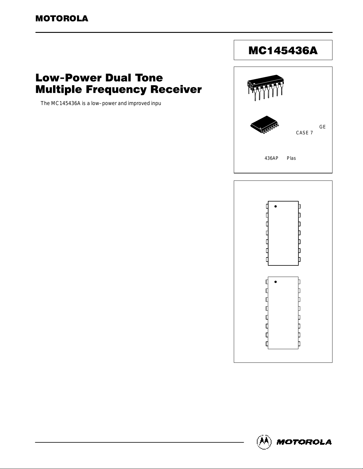
SEMICONDUCTOR TECHNICAL DATA
DW SUFFIX
SOG PACKAGE
CASE 751G
ORDERING INFORMATION
MC145436AP Plastic DIP
MC145436ADW SOG Package
P SUFFIX
PLASTIC DIP
CASE 646
PIN ASSIGNMENTS
NC = NO CONNECTION
PDIP
11
12
13
14
8
9
105
4
3
2
1
7
6
X
in
ATB
DV
D8
D4
GND
X
out
V
DD
ENB
D1
D2
A
in
X
en
GT
13
14
15
16
9
10
11
125
4
3
2
1
8
7
6
ATB
NC
DV
D8
D4
GND
X
out
X
in
V
DD
ENB
D1
D2
A
in
X
en
GT
NC
SOG
16
1
14
1
Motorola, Inc. 1996
REV 1
1/96
Page 2
MC145436A MOTOROLA
2
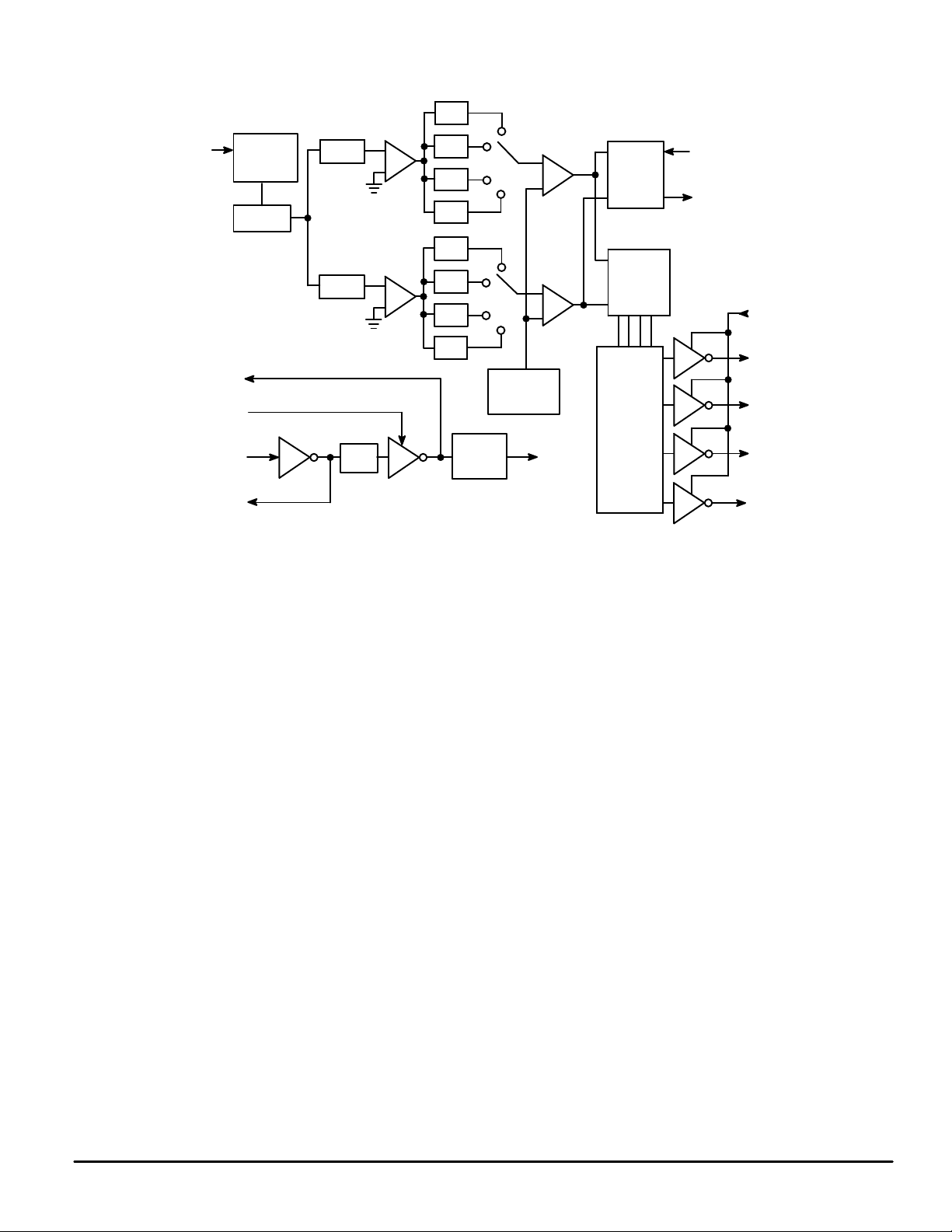
BLOCK DIAGRAM
A
in
60 Hz
REJECTION
FILTER
PREAMP
BS1
BS2
697
770
852
941
1209
1336
1477
1633
TIMING
CIRCUIT
OUTPUT
DECODER
VOLTAGE
REF
OUTPUT
REGISTER
ENB
D1
D2
D4
D8
CHIP
CLOCKS
CLOCK
GEN
÷
8
ATB
X
en
X
in
X
out
GT
DV
Page 3
MC145436AMOTOROLA
3
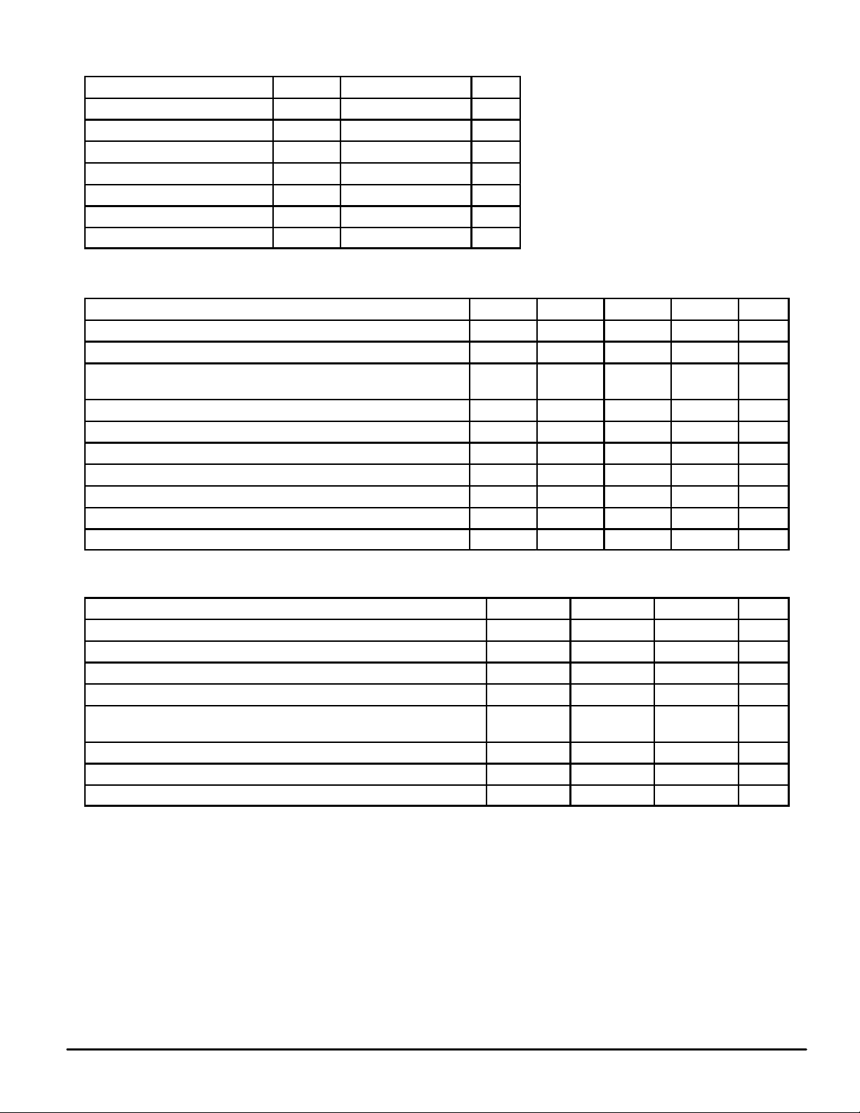
MAXIMUM RATINGS (Voltages Referenced to GND Unless Otherwise Noted)
Rating
Symbol Value Unit
DC Supply Voltage V
DD
– 0.5 to + 6.0 V
Input Voltage, Any Pin Except A
in
V
in
– 0.5 to VDD + 0.5 V
Input Voltage, A
in
V
in
VDD – 10 to VDD + 0.5 V
DC Current Drain per Pin I ± 10 mA
Power Dissipation P
D
100
mW
Operating Temperature Range T
A
– 40 to + 85 °C
Storage Temperature Range T
stg
– 65 to + 150 °C
ELECTRICAL CHARACTERISTICS
(All Polarities Referenced to VSS = 0 V, VDD = 5.0 V ± 10%, TA = – 40 to + 85°C, Unless Otherwise Noted)
Parameter
Symbol Min Typ Max Unit
DC Supply Voltage V
DD
4.5 5 5.5 V
Supply Current (f
CLK
= 3.58 MHz) I
DD
— 5 8 mA
Input Current GT
ENB, Xin, X
en
I
in
—
—
—
—
450
± 1
µA
Input Voltage Low ENB, GT, X
en
V
IL
— — 1.5 V
Input Voltage High ENB, GT, X
en
V
IH
3.5 — — V
I
out
Data and DV Pins: V
out
= 4.5 V (Source) I
OH
800 — — µA
I
out
Data and DV Pins: V
out
= 0.4 V (Sink) I
OL
1.0 — — mA
Input Impedance A
in
R
in
90 100 — kΩ
Fanout ATB F
out
— — 10
Input Capacitance Xen, ENB C
in
— 6 — pF
ANALOG CHARACTERISTICS (V
DD
= 5.0 V ± 10%, TA = – 40 to + 85°C, Unless Otherwise Noted)
Parameter
Min Typ Max Unit
Signal Level for Detection (Ain) – 35 — – 2 dBm
Twist = High Tone/Low Tone – 10 — 10 dB
Frequency Detect Bandwidth ± (1.5 + 2 Hz) ± 2.5 ± 3.5 % f
O
60 Hz Tolerance — — 0.8 Vrms
Dial Tone Tolerance (Note 1)
(Dial Tone 330 + 440)
— — 0 dB
Noise Tolerance (Notes 1 and 2) — — – 12 dB
Power Supply Noise (Wide Band) — — 10 mV p–p
Talk Off (Mitel Tape #CM7290) — 2 — Hits
NOTES:
1. Referenced to lower amplitude tone.
2. Bandwidth limited (0 to 3.4 kHz) Gaussian Noise.
This device contains circuitry to protect the
inputs against damage due to high static voltages or electric fields; however, it is advised that
normal precautions be taken to avoid applications of any voltage higher than the maximum
rated voltages to this high impedance circuit.
For proper operation it is recommended that
Vin and V
out
be constrained to the range VSS ≤
(Vin or V
out
) ≤ VDD. Reliability of operation is
enhanced if unused inputs are tied to and
appropriate logic voltage level (e.g., either V
SS
or VDD).
Page 4

MC145436A MOTOROLA
4
AC CHARACTERISTICS (V
DD
= 5.0 V ± 10%, TA = – 40 to + 85°C)
Characteristic
Symbol Min Typ Max Unit
Tone On Time For Detection
For Rejection
TONE
on
40
—
—
—
—
20
ms
Pause Time For Detection
For Rejection
TONE
off
40
—
—
—
—
20
ms
Detect Time GT = 0
GT = 1
t
det
22
32
—
—
40
50
ms
Release Time GT = 0
GT = 1
t
rel
28
18
—
—
40
30
ms
Data Setup Time t
su
7 — — µs
Data Hold Time t
h
4.2 4.6 5 ms
Pulse Width GT t
w(GT)
18 — — µs
DV Reset Lag Time t
lag(DV)
— — 5 ms
ENB High to Output DV* t
EHDV
— 120 500 ns
ENB Low to Output High–Z* t
ELDZ
— 110 300 ns
*Data out: CL = 35 pF k RL = 500 Ω.
TIMING DIAGRAM
ANALOG INPUT
(Ain)
D1, D2
D4, D8
DV
ENB
GT
TONE
on
TONE BURST 1 TONE BURST 2
t
det
t
rel
HIGH–Z HIGH–Z
t
su
t
h
t
ELDZ
t
EHDV
t
ELDZ
t
lag(DV)
t
w(GT)
TONE
off
Page 5

MC145436AMOTOROLA
5
PIN DESCRIPTIONS
V
DD
Positive Power Supply (PDIP, SOG — Pin 4)
The digital supply pin, which is connected to the positive
side of the power supply.
V
SS
Ground (PDIP — Pin 8, SOG — Pin 9)
Ground return pin is typically connected to the system
ground.
D1, D2, D4, D8
Data Output (PDIP — Pins 2, 1, 14, 13; SOG — Pins 2, 1,
16, 15)
These digital outputs provide the hexadecimal codes corresponding to the detected digit. The digital outputs become
valid after a tone pair has been detected and are cleared
when a valid pause is timed. See Table 1 for hexadecimal
codes.These output p ins are high i mpedance when the
enable pin is at logic 0.
ENB
Enable (PDIP, SOG — Pin 3)
Outputs D1, D2, D4, D8 are enabled when ENB is at a
logic 1, and high impedance (disabled) when ENB is at a
logic 0.
GT
Guard Time (PDIP — Pin 5, SOG — Pin 6)
The guard time control input provides two sets of detected
time and release time, both within the allowed ranges of tone
on and tone off (see Figure 1). A longer tone detect time
rejects signals too short to be considered valid. With GT = 1,
talk off performance is improved, since it reduces the probability that tones simulated by speech will maintain signal
conditions long enough to be accepted. In addition, a shorter
release time reduces the probability that a pause simulated
by an interrupt in speech will be detected as a valid pause.
On the other hand, a shorter tone detect time with a long
Table 1. Hexadecimal Codes
Output Code
Digit
D8 D4 D2 D1
1 0 0 0 1
2 0 0 1 0
3 0 0 1 1
4 0 1 0 0
5 0 1 0 1
6 0 1 1 0
7 0 1 1 1
8 1 0 0 0
9 1 0 0 1
0 1 0 1 0
* 1 0 1 1
# 1 1 0 0
A 1 1 0 1
B 1 1 1 0
C 1 1 1 1
D 0 0 0 0
release time would be appropriate for an extremely noisy
environment where fast acquisition time and immunity to
dropouts would be required. In general, the tone signal time
generated by a telephone is 100 ms, nominal, followed by a
pause of about 100 ms. A high–to–low or low–to–high transition o n the GT p in resets the i nternal logic and t he
MC145436A is immediately ready t o accept a new tone
input. If left open, this pin is internally pulled to ground.
X
en
Oscillator Enable (PDIP — Pin 6, SOG — Pin 7)
A logic 1 on Xen enables the on–chip crystal oscillator.
When using alternate time base from the A TB pin, Xen should
be tied to VSS.
A
in
Analog Input (PDIP — Pin 7, SOG — Pin 8)
This pin accepts the analog input and is internally biased
so that the input signal may be ac coupled. The input may be
dc coupled so long as it does not exceed the positive supply
(see Figure 2).
Xin/X
out
Oscillator In and Oscillator Out (PDIP — Pins 10, 9;
SOG — Pins 11, 10)
These pins connect to an internal crystal oscillator. In operation, a parallel resonant crystal is connected from Xin to
X
out
, as well as a 1 M
Ω resistor in parallel with the crystal.
When using the alternate clock source from ATB, Xin should
be tied to VDD.
ATB
Alternate Time Base (PDIP — Pin 11, SOG — Pin 12)
This pin serves as a frequency reference when more than
one MC145436A is used, so that only one crystal is required
for m ultiple MC145436As. When doing so, a ll ATB pins
should be tied together as shown in Figure 3. When only one
MC145436A is used, this pin should be left unconnected.
The output frequency of ATB is 447.4 kHz.
DV
Data Valid (PDIP — Pin 12, SOG — Pin 14)
DV signals a detection by going high after a valid tone pair
is sensed and decoded at output pins D1, D2, D4, D8. DV
remains high until a loss of the current DTMF signal occurs
or until a transition in GT occurs.
GUARD TIME
V
DD
5
Figure 1. Guard Time
Page 6

MC145436A MOTOROLA
6
A
in
Vin
t
V
DD
V
DD
10 pF
100 k
Ω
0.01 µF
A
in
10 pF
V
DD
100 k
Ω
7 7
Figure 2. Analog Input (Operational Information Based on PDIP Package)
Vin u V
DD
3.58 MHz
X
in
X
out
V
DD
ATB
X
en
1 M
Ω
ATB
X
en
TO OTHER
MC145436As
MC145436A
MC145436A
V
DD
X
in
Figure 3. Multiple MC145436As
COL 1 COL 2 COL 3 COL 4
697
770
852
941
STD
DTMF
(Hz)
ROW 1
ROW 2
ROW 3
ROW 4
1209 1336 1477 1633
1 2 3 A
4 5 6 B
7 8 9 C
*
0 # D
STD DTMF (Hz)
Figure 4. 4 × 4 Keyboard Matrix
Page 7

MC145436AMOTOROLA
7
PACKAGE DIMENSIONS
P SUFFIX
PLASTIC DIP
CASE 646–06
NOTES:
1. LEADS WITHIN 0.13 (0.005) RADIUS OF TRUE
POSITION AT SEATING PLANE AT MAXIMUM
MATERIAL CONDITION.
2. DIMENSION L TO CENTER OF LEADS WHEN
FORMED PARALLEL.
3. DIMENSION B DOES NOT INCLUDE MOLD
FLASH.
4. ROUNDED CORNERS OPTIONAL.
1 7
14 8
B
A
F
H G D
K
C
N
L
J
M
SEATING
PLANE
DIM MIN MAX MIN MAX
MILLIMETERSINCHES
A 0.715 0.770 18.16 19.56
B 0.240 0.260 6.10 6.60
C 0.145 0.185 3.69 4.69
D 0.015 0.021 0.38 0.53
F 0.040 0.070 1.02 1.78
G 0.100 BSC 2.54 BSC
H 0.052 0.095 1.32 2.41
J 0.008 0.015 0.20 0.38
K 0.115 0.135 2.92 3.43
L 0.300 BSC 7.62 BSC
M 0 10 0 10
N 0.015 0.039 0.39 1.01
_ _ _ _
DW SUFFIX
SOG PACKAGE
CASE 751G–02
DIM MIN MAX MIN MAX
INCHESMILLIMETERS
A 10.15 10.45 0.400 0.411
B 7.40 7.60 0.292 0.299
C 2.35 2.65 0.093 0.104
D 0.35 0.49 0.014 0.019
F 0.50 0.90 0.020 0.035
G 1.27 BSC 0.050 BSC
J 0.25 0.32 0.010 0.012
K 0.10 0.25 0.004 0.009
M 0 7 0 7
P 10.05 10.55 0.395 0.415
R 0.25 0.75 0.010 0.029
M
B
M
0.010 (0.25)
NOTES:
1. DIMENSIONING AND TOLERANCING PER ANSI
Y14.5M, 1982.
2. CONTROLLING DIMENSION: MILLIMETER.
3. DIMENSIONS A AND B DO NOT INCLUDE MOLD
PROTRUSION.
4. MAXIMUM MOLD PROTRUSION 0.15 (0.006) PER
SIDE.
5. DIMENSION D DOES NOT INCLUDE DAMBAR
PROTRUSION. ALLOWABLE DAMBAR
PROTRUSION SHALL BE 0.13 (0.005) TOTAL IN
EXCESS OF D DIMENSION AT MAXIMUM
MATERIAL CONDITION.
–A–
–B– P8X
G14X
D16X
SEATING
PLANE
–T–
S
A
M
0.010 (0.25) B
S
T
16 9
81
F
J
R
X 45
_
_ _ _ _
M
C
K
Page 8

MC145436A MOTOROLA
8
Motorola reserves the right to make changes without further notice to any products herein. Motorola makes no warranty, representation or guarantee regarding
the suitability of its products for any particular purpose, nor does Motorola assume any liability arising out of the application or use of any product or circuit,
and specifically disclaims any and all liability, including without limitation consequential or incidental damages. “T ypical” parameters can and do vary in different
applications. All operating parameters, including “T ypicals” must be validated for each customer application by customer’s technical experts. Motorola does
not convey any license under its patent rights nor the rights of others. Motorola products are not designed, intended, or authorized for use as components in
systems intended for surgical implant into the body, or other applications intended to support or sustain life, or for any other application in which the failure of
the Motorola product could create a situation where personal injury or death may occur. Should Buyer purchase or use Motorola products for any such
unintended or unauthorized application, Buyer shall indemnify and hold Motorola and its officers, employees, subsidiaries, affiliates, and distributors harmless
against all claims, costs, damages, and expenses, and reasonable attorney fees arising out of, directly or indirectly, any claim of personal injury or death
associated with such unintended or unauthorized use, even if such claim alleges that Motorola was negligent regarding the design or manufacture of the part.
Motorola and are registered trademarks of Motorola, Inc. Motorola, Inc. is an Equal Opportunity/Affirmative Action Employer.
How to reach us:
USA/EUROPE: Motorola Literature Distribution; JAPAN: Nippon Motorola Ltd.; Tatsumi–SPD–JLDC, Toshikatsu Otsuki,
P.O. Box 20912; Phoenix, Arizona 85036. 1–800–441–2447 6F Seibu–Butsuryu–Center, 3–14–2 Tatsumi Koto–Ku, Tokyo 135, Japan. 03–3521–8315
MFAX: RMFAX0@email.sps.mot.com – TOUCHTONE (602) 244–6609 HONG KONG: Motorola Semiconductors H.K. Ltd.; 8B Tai Ping Industrial Park,
INTERNET: http://Design–NET.com 51 Ting Kok Road, Tai Po, N.T., Hong Kong. 852–26629298
MC145436A/D
*MC145436A/D*
◊
 Loading...