

Page 1
MC145406
1
MOTOROLA
Driver/Receiver
EIA 232–E and CCITT V.28 (Formerly RS–232–D)
The MC145406 is a silicon–gate CMOS IC that combines three drivers
and three receivers to fulfill the electrical specifications of standards
EIA 232–E and CCITT V.28. The drivers feature true TTL input
compatibility, slew–rate–limited output, 300–Ω power–off source imped-
ance, and output typically switching to within 25% of the supply rails. The
receivers can handle up to ±25 V while presenting 3 to 7 kΩ impedance.
Hysteresis in the receivers aids reception of noisy signals. By combining
both drivers and receivers in a single CMOS chip, the MC145406 provides
efficient, low–power solutions for EIA 232–E and V.28 applications.
Drivers
•±
5 V to ±12 V Supply Range
• 300–Ω Power–Off Source Impedance
• Output Current Limiting
• TTL Compatible
• Maximum Slew Rate = 30 V/µs
Receivers
•±
25 V Input Voltage Range When V
DD
= 12 V, VSS = – 12 V
• 3 to 7 kΩ Input Impedance
• Hysteresis on Input Switchpoint
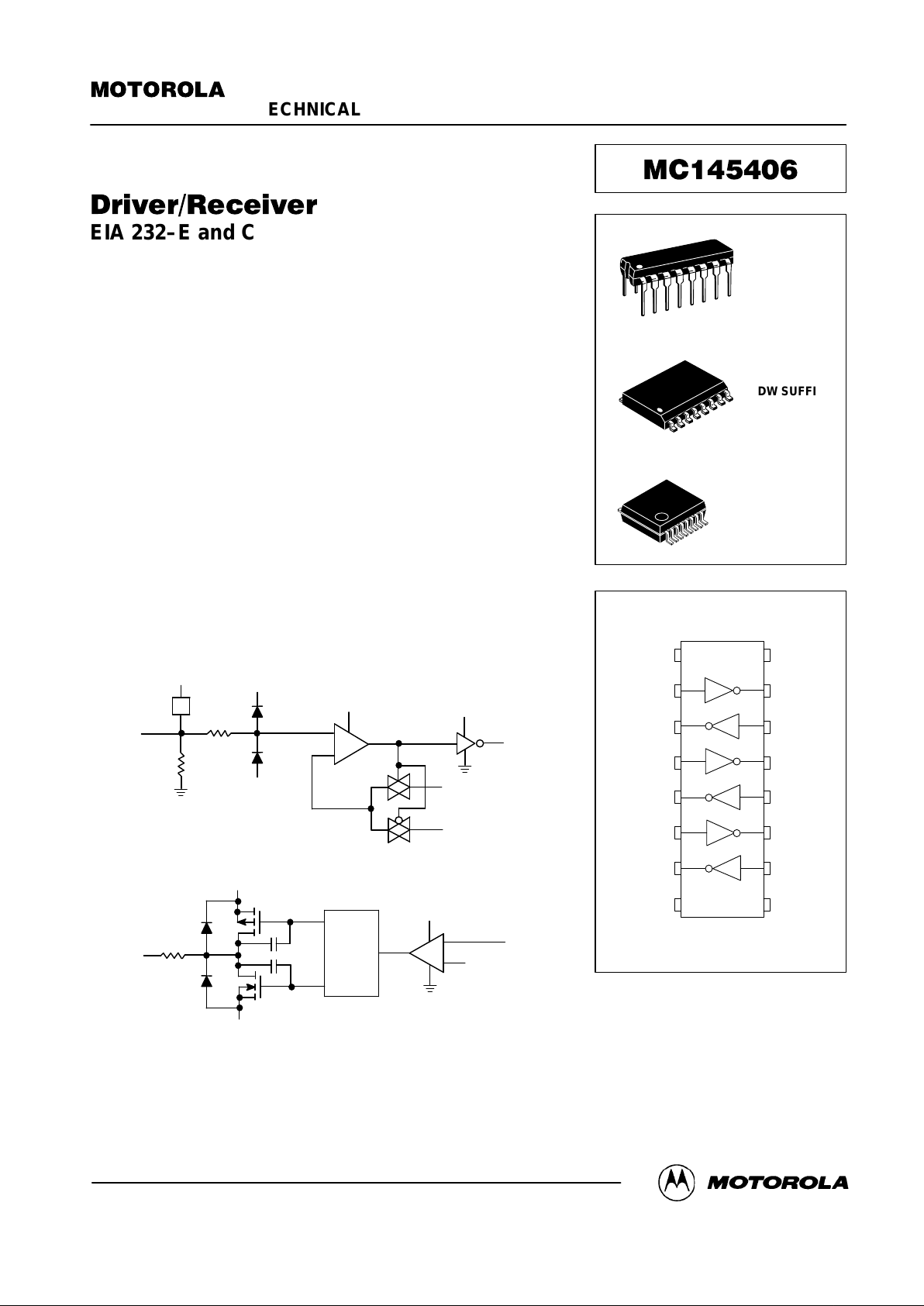
BLOCK DIAGRAM
V
DD
RECEIVER
V
CC
DO
DI
1.4 V
HYSTERESIS
1.8 V
1.0 V
DRIVER
LEVEL
SHIFT
300
Ω
Tx
V
SS
5.4 k
Rx
15 k
Ω
*Protection circuit
V
CC
V
DD
V
DD
V
CC
V
SS
+
–
+
–
*
Order this document
by MC145406/D
MOTOROLA
SEMICONDUCTOR TECHNICAL DATA
PIN ASSIGNMENT
MC145406
P SUFFIX
PLASTIC
CASE 648
DW SUFFIX
SOG
CASE 751G
1
2
3
4
5
6
7
8
9
10
11
12
13
14
15
16
R
D
V
DD
Rx1
Tx1
Rx2
Tx2
Rx3
Tx3
V
SS
V
CC
DO1
DI1
DO2
DI2
DO3
DI3
GND
D = DRIVER
R = RECEIVER
R
R
D
D
16
1
16
1
SD SUFFIX
SSOP
CASE 940B
Motorola, Inc. 1995
REV 4
1/95
Page 2
MC145406
2
MOTOROLA
MAXIMUM RATINGS (Voltage polarities referenced to GND)
Rating Symbol Value Unit
DC Supply Voltages (VDD ≥ VCC) V
DD
V
SS
V
CC
– 0.5 to + 13.5
+ 0.5 to – 13.5
– 0.5 to + 6.0
V
Input Voltage Range
Rx1–3 Inputs
DI1–3 Inputs
V
IR
(VSS – 15) to (VDD + 15)
– 0.5 to (VCC + 0.5)
V
DC Current Per Pin
± 100
mA
Power Dissipation P
D
1.0 W
Operating Temperature Range T
A
– 40 to + 85 °C
Storage Temperature Rate T
stg
– 85 to + 150 °C
DC ELECTRICAL CHARACTERISTICS (All polarities referenced to GND = 0 V , T
A
= – 40 to +85°C)
Parameter
Symbol Min Typ Max Unit
DC Supply Voltage
V
DD
V
SS
VCC (VDD ≥ VCC)
V
DD
V
SS
V
CC
4.5
–
4.5
4.5
5 to 12
–
5 to – 12
5.0
13.2
–
13.2
5.5
V
Quiescent Supply Current (Outputs unloaded, inputs low)
VDD = + 12 V
VSS = –
12 V
VCC = + 5 V
I
DD
I
SS
I
CC
—
—
—
140
340
300
400
600
450
µA
RECEIVER ELECTRICAL SPECIFICATIONS
(Voltage polarities referenced to GND = 0 V, VDD = + 5 to + 12 V, VSS = – 5 to – 12 V, VDD ≥ VCC, TA = – 40 to + 85°C)
Characteristic
Symbol Min Typ Max Unit
Input Turn–on Threshold Rx1–Rx3
V
DO1–DO3
= VOL, VCC = 5.0 V ±
5%
V
on
1.35 1.80 2.35 V
Input Turn–off Threshold Rx1–Rx3
V
DO1–DO3
= VOH, VCC = 5.0 V ± 5%
V
off
0.75 1.00 1.25 V
Input Threshold Hysteresis Rx1–Rx3
VCC = 5.0 V
± 5%
Von–V
off
0.6 0.8 — V
Input Resistance Rx1–Rx3
(VSS –
15 V) ≤ V
Rx1–Rx3
≤ (VDD + 15 V)
R
in
3.0 5.4 7.0 kΩ
High–Level Output Voltage (V
Rx1–Rx3
= – 3 V to (VSS – 15 V))*
DO1–DO3
IOH = – 20 µA, VCC = +
5.0 V
IOH = –1 mA, VCC = +
5.0 V
V
OH
4.9
3.8
4.9
4.3
—
—
V
Low–Level Output Voltage (V
Rx1–Rx3
= + 3 V to (VDD + 15 V))* DO1–DO3
IOL = +
20 µA, V
CC
= + 5.0 V
IOL = +
2 mA, V
CC
= + 5.0 V
IOL = + 4 mA, VCC = + 5.0 V
V
OL
—
—
—
0.01
0.02
0.5
0.1
0.5
0.7
V
* This is the range of input voltages as specified by EIA 232–E to cause a receiver to be in the high or low logic state.
This device contains protection circuitry to protect the inputs against damage due to high static
voltages or electric fields; however, it is advised
that normal precautions be taken to avoid application of any voltage higher than maximum rated
voltages to this high impedance circuit. For proper
operation, it is recommended that the voltages at
the DI and DO pins be constrained to the range
GND ≤VDI≤ VCC and GND≤ VDO ≤ VCC. Also, the
voltage at the Rx pin should be constrained to
(VSS – 15 V) ≤ V
Rx1–3
≤ (VDD + 15 V), and Tx
should be constrained to VSS ≤ V
Tx1–3
≤ VDD.
Unused inputs must always be tied to an appropriate logic voltage level (e.g., GND or VCC for
DI and Ground for Rx.)
Page 3
MC145406
3
MOTOROLA
ELECTRICAL SPECIFICATIONS (Voltage polarities referenced to GND = 0 V, V
CC
= + 5 V ± 5%, TA = – 40 to + 85°C)
Characteristic
Symbol Min Typ Max Unit
Digital Input Voltage DI1–DI3
Logic 0
Logic 1
V
IL
V
IH
—
2.0
—
—
0.8
—
V
Input Current DI1–DI3
V
DI1–DI3
= V
CC
I
in
— — ± 1.0 µA
Output High Voltage (V
DI1–3
= Logic 0, RL = 3.0 kΩ) Tx1–Tx3
VDD = + 5.0 V, VSS = –
5.0 V
VDD = + 6.0 V, VSS = – 6.0
VDD = +
12.0 V, V
SS
= – 12.0 V
V
OH
3.5
4.3
9.2
3.9
4.7
9.5
—
—
—
V
Output Low Voltage* (V
DI1–3
= Logic 1, RL = 3.0 kΩ) Tx1–Tx3
VDD = + 5.0 V, VSS = – 5.0 V
VDD = + 6.0 V, VSS = – 6.0 V
VDD = +
12.0 V, V
SS
= – 12.0 V
V
OL
– 4.0
–
4.5
–
10.0
– 4.3
–
5.2
– 10.3
—
—
—
V
Off Source Resistance (Figure 1) Tx1–Tx3
VDD = VSS = GND = 0 V, V
Tx1–Tx3
= ±
2.0 V
300 — — Ω
Output Short–Circuit Current (VDD = + 12.0 V, VSS = – 12.0 V) Tx1–Tx3
Tx1–Tx3 shorted to GND**
Tx1–Tx3 shorted to ±
15.0 V***
I
SC
—
—
± 22
±
60
± 60
±
100
mA
*The voltage specifications are in terms of absolute values.
**Specification is for one Tx output pin to be shorted at a time. Should all three driver outputs be shorted simultaneously, device power dissipation
limits will be exceeded.
***This condition could exceed package limitations.
SWITCHING CHARACTERISTICS (V
CC
= + 5 V ± 5%, TA = – 40 to + 85°C; See Figures NO TAG and NO TAG)
Drivers
Characteristic Symbol Min Typ Max Unit
Propagation Delay Time Tx1–Tx3
Low–to–High
RL = 3 kΩ, CL = 50 pF
t
PLH
— 300 500
ns
High–to–Low
RL = 3 kΩ CL = 50 pF
t
PHL
— 300 500
Output Slew Rate Tx1–Tx3
Minimum Load
RL = 7 kΩ, CL = 0 pF, VDD = +
6 to + 12 V, V
SS
= – 6 to – 12 V
SR
— ± 9 ± 30
V/µs
Maximum Load
RL = 3 kΩ, CL = 2500 pF
VDD = + 12 V, VSS = – 12 V
VDD = + 5 V, VSS = – 5 V
4
—
—
—
—
—
Receivers (CL = 50 pF)
Characteristic Symbol Min Typ Max Unit
Propagation Delay Time DO1–DO3
Low–to–High
t
PLH
— 150 425
ns
High–to–Low t
PHL
— 150 425
Output Rise Time DO1–DO3 t
r
— 250 400 ns
Output Fall Time DO1–DO3 t
f
— 40 100 ns
Page 4
MC145406
4
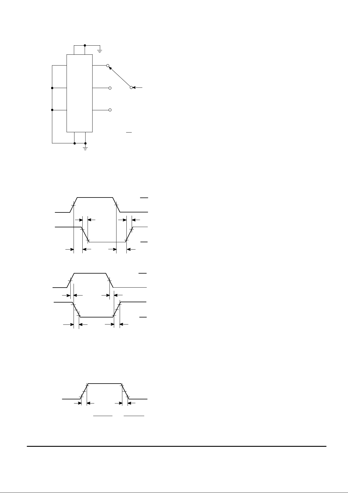
MOTOROLA
Vin = ± 2
V
3
5
7
14
12
10
89
116
VDDV
CC
DI1
DI2
DI3
V
SS
GND
Tx3
Tx2
Tx1
R
out
=
V
in
I
Figure 1. Power–Off Source Resistance (Drivers)
Figure 2. Switching Characteristics
Figure 3. Slew–Rate Characterization
DRIVERS
DI1–DI3
3 V
0 V
V
OH
V
OL
Tx1–Tx3
t
PLH
t
PHL
50%
t
f
t
r
10%
90%
RECEIVERS
Rx1–Rx3
DO1–DO3
+ 3 V
0 V
V
OH
V
OL
t
PLH
t
PHL
t
f
t
r
50%
DRIVERS
Tx1–Tx3
90%
50%
3 V
– 3 V
3 V
– 3 V
t
SHL
t
SLH
SLEW RATE (SR) =
– 3 V – (3 V)OR3 V – ( – 3 V)
t
SLH
t
SHL
10%
PIN DESCRIPTIONS
V
DD
Positive Power Supply (Pin 1)
The most positive power supply pin, which is typically + 5
to +
12V.
V
SS
Negative Power Supply (Pin 8)
The most negative power supply pin, which is typically – 5
to –
12 V.
V
CC
Digital Power Supply (Pin 16)
The digital supply pin, which is connected to the logic
power supply (maximum +
5.5 V). V
CC
must
be less than
or equal to VDD.
GND
Ground (Pin 9)
Ground return pin is typically connected to the signal
ground pin of the EIA 232–E connector (Pin 7) as well as to
the logic power supply ground.
Rx1, Rx2, Rx3
Receive Data Input (Pins 2, 4, 6)
These are the EIA 232–E receive signal inputs whose
voltages can range from (VDD + 15 V) to (VSS – 15 V). A voltage between +
3 and (V
DD
+ 15 V) is decoded as a space
and causes the corresponding DO pin to swing to ground (0
V); a voltage between – 3 and (VDD – 15 V) is decoded as a
mark and causes the DO pin to swing up to VCC. The actual
turn–on input switchpoint is typically biased at 1.8 V above
ground, and includes 800 mV of hysteresis for noise rejection. The nominal input impedance is 5 kΩ. An open or
grounded input pin is interpreted as a mark, forcing the DO
pin to VCC.
DO1, DO2, DO3
Data Output (Pins 11, 13, 15)
These are the receiver digital output pins, which swing
from VCC to GND. A space on the Rx pin causes DO to produce a logic 0; a mark produces a logic 1. Each output pin is
capable of driving one LSTTL input load.
DI1, DI2, DI3
Data Input (Pins 10, 12,14)
These are the high–impedance digital input pins to the
drivers. TTL compatibility is accomplished by biasing the input switchpoint at 1.4 V above GND. However, 5–V CMOS
compatibility is maintained as well. Input voltage levels on
these pins must be between VCC and GND.
Tx1, Tx2, Tx3
Transmit Data Output(Pins 3, 5, 7)
These are the EIA 232–E transmit signal output pins,
which swing toward VDD and VSS. A logic 1 at a DI input
causes the corresponding Tx output to swing toward VSS. A
logic 0 causes the output to swing toward VDD (the output
voltages will be slightly less than VDD or VSS depending upon
the output load). Output slew rates are limited to a maximum
of 30 V per µs. When the MC145406 is off (VDD = VSS = V
CC
= GND), the minimum output impedance is 300 Ω.
Page 5

MC145406
5
MOTOROLA
APPLICATIONS INFORMATION
The MC145406 has been designed to meet the electrical
specifications of standards EIA 232–E and CCITT V.28.
EIA 232–E defines the electrical and physical interface between Data Communication Equipment (DCE) and Data
Terminal Equipment (DTE). A DCE is connected to a DTE
using a cable that typically carries up to 25 leads. These
leads, referred to as interchange circuits, allow the transfer
of timing, data, control, and test signals. Electrically this
transfer requires level shifting between the TTL/CMOS logic levels of the computer or modem and the high voltage levels of EIA 232–E, which can range from ±
3 to ± 25 V. The
MC145406 provides the necessary level shifting as well as
meeting other aspects of the EIA 232–E specification.
DRIVERS
As defined by the specification, an EIA 232–E driver presents a voltage of between ± 5 to ± 15 V into a load of between 3 to 7 kΩ. A logic 1 at the driver input results in a
voltage of between –
5 to – 15 V. A logic 0 results in a voltage
between + 5 to + 15V. When operating VDD and VSS at ± 7 to
± 12 V , the MC145406 meets this requirement. When operating at ± 5 V, the MC145406 drivers produce less than
± 5 V at the output (when terminated), which does not meet
EIA 232–E specification. However, the output voltages when
using a ± 5 V power supply are high enough (around
± 4 V) to permit proper reception by an EIA 232–E receiver,
and can be used in applications where strict compliance to
EIA 232–E is not required.
Another requirement of the MC145406 drivers is that
they withstand a short to another driver in the EIA 232–E
cable. The worst–case condition that is permitted by
EIA 232–E is a ± 15 V source that is current limited to 500
mA. The MC145406 drivers can withstand this condition
momentarily. In most short circuit conditions the source
driver will have a series 300 Ω output impedance needed
to satisfy the EIA 232–E driver requirements. This will reduce the short circuit current to under 40 mA which is an
acceptable level for the MC145406 to withstand.
Unlike some other drivers, the MC145406 drivers feature
an internally–limited output slew–rate that does not exceed
30 V per µs.
RECEIVERS
The job of an EIA 232–E receiver is to level–shift voltages
in the range of – 25 to + 25 V down to TTL/CMOS logic levels (0 to + 5 V). A voltage of between – 3 and – 25 V on Rx1
is defined as a mark and produces a logic 1 at DO1. A voltage between + 3 and + 25 V is a space and produces a logic
zero. While receiving these signals, the Rx inputs must present a resistance between 3 and 7 kΩ. Nominally, the input resistance of the Rx1–Rx3 inputs is 5.4 kΩ.
The input threshold of the Rx1–Rx3 inputs is typically
biased at 1.8 V above ground (GND) with typically 800 mV of
hysteresis included to improve noise immunity. The 1.8 V
bias forces the appropriate DO pin to a logic 1 when its Rx
input is open or grounded as called for in the EIA 232–E
specification. Notice that TTL logic levels can be applied to
the Rx inputs in lieu of normal EIA 232–E signal levels. This
might be helpful in situations where access to the modem or
computer through the EIA 232–E connector is necessary
with TTL devices. However, it is important not to connect the
EIA 232–E outputs (Tx1–Tx3) to TTL inputs since TTL operates off + 5 V only, and may be damaged by the high output
voltage of the MC145406.
The DO outputs are to be connected to a TTL or CMOS
input (such as an input to a modem chip). These outputs
will swing from VCC to ground, allowing the designer to op erate the DO and DI pins from digital power supply. The Tx
and Rx sections are independently powered by VDD and
VSS so that one may run logic at + 5 V and the EIA 232–E
signals at ± 12 V.
POWER SUPPLY CONSIDERATIONS
Figure 4 shows a technique to guard against excessive
device current.
The diode D1 prevents excessive current from flowing
through an internal diode from the VCC pin to the VDD pin
when VDD < VCC by approximately 0.6 V . This high current
condition can exist for a short period of time during power
up/down. Additionally, if the + 12 V supply is switched off
while the + 5 V is on and the off supply is a low impedance
to ground, the diode D1 will prevent current flow through
the internal diode.
The diode D2 is used as a voltage clamp, to prevent V
SS
from drifting positive to VCC, in the event that power is removed from VSS (Pin 12). If VSS power is removed, and the
impedance from the VSS pin to ground is greater than
approximately 3 kΩ, this pin will be pulled to VCC by internal
circuitry causing excessive current in the VCC pin.
If by design, neither of the above conditions are allowed
to exist, then the diodes D1 and D2 are not required.
ESD PROTECTION
ESD protection on IC devices that have their pins accessible to the outside world is essential. High static voltages applied to the pins when someone touches them either directly
or indirectly can cause damage to gate oxides and transistor
junctions by coupling a portion of the energy from the I/O pin
to the power supply buses of the IC. This coupling will usually
occur through the internal ESD protection diodes. The key to
protecting the IC is to shunt as much of the energy to ground
as possible before it enters the IC. Figure 4 shows a technique which will clamp the ESD voltage at approximately ±
15 V using the MMVZ15VDLT1. Any residual voltage which
appears on the supply pins is shunted to ground through the
capacitors C1–C3. This scheme has provided protection to
the interface part up to ± 10 kV , using the human body model
test.
Page 6

MC145406
6
MOTOROLA
0.1 µF
V
CC
0.1 µF
V
DD
MC145406
116
215
314
413
512
611
710
89
V
SS
0.1 µF
RxI
TxO
RxI
TxO
RxI
TxO
TO
CONNECTOR
MMBZ15VDLT × 6
IN4001
IN5818
D1
C1 C2
D2
C3
Figure 4. ESD and Power Supply Networks
Page 7

MC145406
7
MOTOROLA
17
20 k
Ω
NC
DO3
10
µ
F
R
TLA**
DTMF
INPUT
R
DSI
20 k
Ω
C
DSI
6
9
1
15
8
3.579
MHz
3
11
5
14
2
13
7
12
4
19
10
18
16
V
DD
TLA
DSI
X
in
X
out
CD
TxD
TxA
RxA2
RxA1
ExI
FB
V
AG
CDT GND CDA
LB
SQT
RxD
R
Tx
600
+
10 k
Ω
TIP
600:600
RING
V
DD
VDD BYPASS
C
FB
MODE
+ 5 V
1
MC145442/3
10 k
Ω
10 k
Ω
C
CDA**
0.1
µ
F
C
CDT
VSS BYPASS
14
15
12
13
10
11
89
6
7
4
5
2
3
8
2
3
7
EIA 232–E
DB–25
CONNECTOR
NC
NC
V
SS
GND
DI3
DO2
DI2
DO1
DI1
V
DDVCC
MC145406
Tx1
Rx1
Tx2
Rx2
Tx3
Rx3
16
– 5 V
*Line protection circuit
**Refer to the applications information for values of C
CDA
and R
TLA
0.1 µF0.1 µF
0.1
µ
F
0.1
µ
F
0.1
µ
F
10 k
10 k
Ω
*
0.1 µF
0.1 µF
0.1 µF
Figure 5. 5–V 300–Baud Modem with EIA 232–E Interface
Page 8

MC145406
8
MOTOROLA
123
456
789
0*#
TWISTED
PAIR
MC34119
SPEAKER
DRIVER
MC145412/13/16
PULSE/TONE
DIALER
HOOKSWITCH
MC145503
FILTER/
CODEC
RINGING
MC145426
UDLT
LINE
INTERFACE
(TRANSFORMER
AND
PROTECTION)
CONNECTION
TO EXTERNAL
TERMINAL
OR PC
MC145406
RS–232
DRIVER
RECEIVER
MC145428
DATA
SET
INTERFACE
+ 5 V
GND
– 5 V
MC34129
SWITCHING
POWER
SUPPLY
(ISOLATED)
LINE
FILTER
SYNC
Figure 6. Line–Powered Voice/Data Telephone with Electrically Isolated EIA 232–E Interface
Page 9

MC145406
9
MOTOROLA
CC
V
CC
V
CC
V
CC
V
DD
V
CC
V
CC
V
DD
V
DD
V
DD
V
DD
V
DD
V
SS
V
SS
V
SS
V
SS
V
SS
V
IN1
ref
V
0.1
µ
F
0.1
µ
F 0.1
µ
F
1.0
µ
F**
0.1
µ
F
0.1
µ
F
R5
6
DSR
Tx
RTS
CD
CTS
Rx
SG
2
4
853
7
C14
DB-25
CC
V
MC145406
Rx1
Rx2
Rx3
Tx1
Tx2
Tx3
DO1
DO2
DO3
DI1
DI2
DI3
1
8246357
9
16151311121014
NC
NC
NCNCNC
NC
R1 S1
GND
D2
Q1Q1
Q2Q
Q1
D1Q2S2
C2
1
4
13 3
14
7
12
562891011
NC
NC
ST
ST
STSTST
ST
MC74HC74
RxS BC
TxD
DL
BRCLK
RxD
BR1
BR2
BR3
SB
TxS
RESET
DCO
DOE
DC
DIE
DCI
CM
MC145428
12 5
20
16
13
14
15
17
18
19
1
2
3
4
11
678
9
10
0.1
µ
F
NCNC
OUT4
OUT2
IN4
IN3
OUT3
OUT1
OUT6 IN6 IN5OUT5
IN2
MC14069UB
8 9 14 7
4
5
6
1
2
3
12 10 13 11
20 pF
20 pF
10 M
4.096
MHz
2.048 MHz
128 kHz
8 MHz
1000
pF*
NC NC NC
NC
NC
NC
b
Q
a
Q1
C
a
a
Q2
a
Q3
bQ1bQ2b
Q3
b
Q4
a
Q4
a
R
b
Q2
GND
MC74HC393
345
1142
7
12
11
10
9
613 8
NCST ST
4.096 MHz
21
20
1819171412
15
11 16 9 8 5 4
7 6 3 10 22 2 1 13
Rx
RE1
TDC/RDC
TE1
MSI
Tx
LO1
LO2
SO1 SI1L1
SE SIE
LB
PD CCI SO2 SI2VD
MC145422
D1
D2
10 k
220 220
TIP
RING
TR1
NCNC
T1
89
7
6
5
10
1
2
3
4
*For optional filtering.
**TR1 should be cut when this capacitor is used.
ST — STRAP
NC — NO CONNECTION
= 5 V
GND = 0 V
AND
CCVDD
V
ARE DISCUSSED IN THE EIA-232-D SECTION
SS
V
GND
C1R2
Figure 7. 80–kbps Limited Distance Modem with EIA 232–E Interface (Master)
Page 10

MC145406
10
MOTOROLA
P ACKAGE DIMENSIONS
P SUFFIX
CASE 648–08
MIN MINMAX MAX
INCHES MILLIMETERS
DIM
A
B
C
D
F
G
H
J
K
L
M
S
18.80
6.35
3.69
0.39
1.02
0.21
2.80
7.50
0
°
0.51
19.55
6.85
4.44
0.53
1.77
0.38
3.30
7.74
10
°
1.01
0.740
0.250
0.145
0.015
0.040
0.008
0.110
0.295
0
°
0.020
0.770
0.270
0.175
0.021
0.070
0.015
0.130
0.305
10
°
0.040
NOTES:
1. DIMENSIONING AND TOLERANCING PER ANSI
Y14.5M, 1982.
2. CONTROLLING DIMENSION: INCH.
3. DIMENSION L TO CENTER OF LEADS WHEN
FORMED PARALLEL.
4. DIMENSION B DOES NOT INCLUDE MOLD FLASH.
5. ROUNDED CORNERS OPTIONAL.
2.54 BSC
1.27 BSC
0.100 BSC
0.050 BSC
STYLE 1:
PIN 1. CATHODE
2. CATHODE
3. CATHODE
4. CATHODE
5. CATHODE
6. CATHODE
7. CATHODE
8. CATHODE
9. ANODE
10. ANODE
11. ANODE
12. ANODE
13. ANODE
14. ANODE
15. ANODE
16. ANODE
STYLE 2:
PIN 1. COMMON DRAIN
2. COMMON DRAIN
3. COMMON DRAIN
4. COMMON DRAIN
5. COMMON DRAIN
6. COMMON DRAIN
7. COMMON DRAIN
8. COMMON DRAIN
9. GATE
10. SOURCE
11. GATE
12. SOURCE
13. GATE
14. SOURCE
15. GATE
16. SOURCE
-A-
B
18
916
F
H
G
D
16 PL
S
C
-T-
SEATING
PLANE
K
J
M
L
TA0.25 (0.010)
M M
DW SUFFIX
CASE 751G–02
18
916
MIN MINMAX MAX
MILLIMETERS INCHES
DIM
A
B
C
D
F
G
J
K
M
P
R
10.15
7.40
2.35
0.35
0.50
0.25
0.10
0
°
10.05
0.25
10.45
7.60
2.65
0.49
0.90
0.32
0.25
7
°
10.55
0.75
0.400
0.292
0.093
0.014
0.020
0.010
0.004
0
°
0.395
0.010
0.411
0.299
0.104
0.019
0.035
0.012
0.009
7
°
0.415
0.029
1.27 BSC 0.050 BSC
-A-
-B-
P 8 PL
G 14 PL
-T-
D
16 PL
K
C
SEATING
PLANE
M
R
X 45°
0.25 (0.010)
B
M M
0.25 (0.010) T A B
M
S S
NOTES:
1. DIMENSIONING AND TOLERANCING PER
ANSI Y14.5M, 1982.
2. CONTROLLING DIMENSION: MILLIMETER.
3. DIMENSIONS A AND B DO NOT INCLUDE
MOLD PROTRUSION.
4. MAXIMUM MOLD PROTRUSION 0.15 (0.006)
PER SIDE.
5. DIMENSION D DOES NOT INCLUDE
DAMBAR PROTRUSION. ALLOWABLE
DAMBAR PROTRUSION SHALL BE 0.13
(0.005) TOTAL IN EXCESS OF D DIMENSION
AT MAXIMUM MATERIAL CONDITION.
F
J
Page 11

MC145406
11
MOTOROLA
SD SUFFIX
CASE 940B–02
DIMAMIN MAX MIN MAX
INCHES
6.10 6.30 0.240 0.248
MILLIMETERS
B 5.20 5.38 0.205 0.212
C 1.75 1.99 0.069 0.078
D 0.25 0.38 0.010 0.015
F 0.65 1.00 0.026 0.039
G 0.65 BSC 0.026 BSC
H 0.73 0.90 0.029 0.035
J 0.10 0.20 0.004 0.008
L 7.65 7.90 0.301 0.311
M 0 8 0 8
N 0.05 0.21 0.002 0.008
____
NOTES:
1. DIMENSIONING AND TOLERANCING PER ANSI
Y14.5M, 1982.
2. CONTROLLING DIMENSION: MILLIMETER.
3. DIMENSIONS A AND B DO NOT INCLUDE
MOLD FLASH OR PROTRUSIONS AND ARE
MEASURED AT THE PARTING LINE. MOLD FLASH
OR PROTRUSIONS SHALL NOT EXCEED 0.15
(0.006) PER SIDE.
4. DIMENSION IS THE LENGTH OF TERMINAL
FOR SOLDERING TO A SUBSTRATE.
5. TERMINAL POSITIONS ARE SHOWN FOR
REFERENCE ONLY.
6. THE LEAD WIDTH DIMENSION DOES NOT
INCLUDE DAMBAR PROTRUSION. ALLOWABLE
DAMBAR PROTRUSION SHALL BE 0.08 (0.003)
TOTAL IN EXCESS OF THE LEAD WIDTH
DIMENSION.
-T-
H
G
D
0.120 (0.005)MTP
S
N
C
A
B
0.076 (0.003)
-R-
-P-
16 8
71
L
0.250 (0.010)MR
M
F
J
M
NOTE 4
Page 12

MC145406
12
MOTOROLA
Motorola reserves the right to make changes without further notice to any products herein. Motorola makes no warranty, representation or guarantee regarding
the suitability of its products for any particular purpose, nor does Motorola assume any liability arising out of the application or use of any product or circuit,
and specifically disclaims any and all liability, including without limitation consequential or incidental damages. “T ypical” parameters can and do vary in different
applications. All operating parameters, including “T ypicals” must be validated for each customer application by customer’s technical experts. Motorola does
not convey any license under its patent rights nor the rights of others. Motorola products are not designed, intended, or authorized for use as components in
systems intended for surgical implant into the body, or other applications intended to support or sustain life, or for any other application in which the failure of
the Motorola product could create a situation where personal injury or death may occur. Should Buyer purchase or use Motorola products for any such
unintended or unauthorized application, Buyer shall indemnify and hold Motorola and its officers, employees, subsidiaries, affiliates, and distributors harmless
against all claims, costs, damages, and expenses, and reasonable attorney fees arising out of, directly or indirectly, any claim of personal injury or death
associated with such unintended or unauthorized use, even if such claim alleges that Motorola was negligent regarding the design or manufacture of the part.
Motorola and are registered trademarks of Motorola, Inc. Motorola, Inc. is an Equal Opportunity/Affirmative Action Employer.
MC145406/D
*MC145406/D*
◊
CODELINE TO BE PLACED HERE
Literature Distribution Centers:
USA: Motorola Literature Distribution; P.O. Box 20912; Phoenix, Arizona 85036.
EUROPE: Motorola Ltd.; European Literature Centre; 88 T anners Drive, Blakelands, Milton Keynes, MK14 5BP, England.
JAPAN: Nippon Motorola Ltd.; 4-32-1, Nishi-Gotanda, Shinagawa-ku, Tokyo 141, Japan.
ASIA PACIFIC: Motorola Semiconductors H.K. Ltd.; Silicon Harbour Center , No. 2 Dai King Street, T ai Po Industrial Estate, Tai Po, N.T., Hong Kong.
 Loading...