

Page 1
INTEGRATED CIRCUITS
MC145406
EIA-232-D/V.28 driver/receiver
Product specification
IC19 Data Handbook
1994 Aug 31
Page 2
Philips Semiconductors Product specification
MC145406EIA-232-D/V.28 driver/receiver
DESCRIPTION
The MC145406 is a silicon-gate CMOS IC that combines 3 drivers
and 3 receivers to fulfill the electrical specifications of standards
EIA-232-D and CCITT V .28. The drivers feature true TTL input
compatibility , slew-rate limited output, 300Ω power-off source
impedance, and output typically switching to within 25% of the
supply rails. The receivers can handle up to ±25V while presenting
3 to 7kΩ impedance. Hysteresis in the receiver aids reception of
noisy signals. By combining both drivers and receivers in a single
CMOS chip, the MC145406 provides efficient, low-power solutions
for EIA-232-D and V .28 applications.
FEATURES
Drivers
•±5 to ±12V supply range
•300Ω power-off source impedance
•Output current limiting
•TTL compatible
•Maximum slew rate = 30V/µs
Receivers
•±25V input voltage range over the full supply range
•3 to 7kΩ input impedance
•Hysteresis on input switchpoint
General
•Very low supply currents for long battery life
•Operation is independent of power supply sequencing
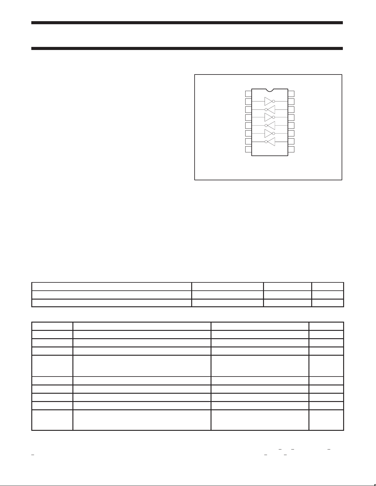
PIN CONFIGURATION
D and N Packages
V
DD
1
RX
2
1
TX
3
1
RX
2
4
TX
2
5
RX
6
3
TX
3
7
V
8
SS
NOTE:
D = Driver
R = Receiver
Figure 1. Pin Configuration
APPLICATIONS
•Modem interface
•Voice/data telephone interface
•Lap-top computers
•UART interface
V
16
CC
R
R
R
15
DO1
14
D
D
D
DI1
13
DO2
12
DI2
11
DO3
10
DI3
GND
9
SL00057
ORDERING INFORMATION
DESCRIPTION TEMPERATURE RANGE ORDER CODE DWG #
16-Pin Plastic Dual In-Line (DIP) Package 0 to +70°C MC145406N SOT38-4
16-Pin Small Outline Large (SOL) Package 0 to +70°C MC145406D SOT162-1
ABSOLUTE MAXIMUM RATINGS
SYMBOL PARAMETER RATING UNITS
V
CC
V
DD
V
SS
V
IR
P
D
T
A
T
STG
θ
JA
NOTE: This device contains protection circuitry to protect the inputs against damage due to high static voltages or electric fields; however, it is
advised that normal precautions be taken to avoid application of any voltage higher than maximum rated voltages to this high impedance circuit.
For proper operation, it is recommended that the voltages at the DI and DO pins be constrained to the range GND ≤
≤ VCC. Also, the voltage at the RX pin should be constrained to ±25V, and TX should be constrained to VSS ≤ V
always be tied to an appropriate logic voltage level (e.g., GND or V
Supply voltage -0.5 to +6.0 V
Supply voltage -0.5 to +13.5 V
Supply voltage +0.5 to -13.5 V
Input voltage range
RX
inputs (VSS - 15) to (VDD + 15) V
1-3
DI
inputs -0.5 to (VCC + 0.5) V
1-3
DC current per pin ±100 mA
Power dissipation (package) 1.0 W
Operating temperature range 0 to +70 °C
Storage temperature range -65 to +150 °C
Thermal impedance
N package 80 °C/W
D package 105 °C/W
VDI ≤ VDD and GND ≤ V
≤ VDD. Unused inputs must
for DI, and VSS or VDD for RX).
CC
TX1-3
DO
1994 Aug 31 853-1430 13721
2
Page 3

Philips Semiconductors Product specification
MC145406EIA-232-D/V.28 driver/receiver
BLOCK DIAGRAM
RX
TX
300
5.4k
RECEIVER
15k
V
SS
V
DD
V
SS
DRIVER
LEVEL
SHIFT
V
CC
+
–
HYSTERESIS
V
CC
V
CC
DO
1.0V
1.8V
+
–
1.4V
DI
SL00058
Figure 2. Block Diagram
PIN #
1 V
8 V
16 V
SYMBOL PIN DESCRIPTION
DD
SS
CC
Positive power supply. The most positive power supply pin, which is typically 5 to 12 volts.
Negative power supply. The most negative power supply pin, which is typically -5 to -12 volts.
Digital power supply. The digital supply pin, which is connected to the logic power supply (maximum +5.5V).
9 GND Ground. Ground return pin is typically connected to the signal ground pin of the EIA-232-D connector (Pin 7)
as well as to the logic power supply ground.
2, 4, 6 RX1, RX2, RX3Receive Data Input. These are the EIA-232-D receive signal inputs whose voltages can range from +25 to
-25V . A voltage between +3 and +25 is decoded as a space and causes the corresponding DO pin to swing to
ground (0V); a voltage between -3 and -25V is decoded as a mark and causes the DO pin to swing up to V
The actual turn-on input switchpoint is typically biased at 1.8V above ground, and includes 800mV of hysteresis
CC
for noise rejection. The nominal input impedance is 5kΩ. An open or grounded input pin is interpreted as a mark,
forcing the DO pin to V
CC
.
11, 13, 15 DO1, DO2, DO3 Data Output. These are the receiver digital output pins, which swing from VCC to GND. A space on the RX pin
causes DO to produce a logic zero; a mark produces a logic one. Each output pin is capable of driving one
LSTTL input load.
10, 12, 14 DI1, DI2, DI3 Data Input. These are the high-impedance digital input pins to the drivers. TTL compatibility is accomplished
by biasing the input switchpoint at 1.4V above ground. However, 5V CMOS compatibility is maintained as well.
Input voltage levels on these pins must be between VCC and GND.
3, 5, 7 TX1, TX2, TX3 Transmit Data Output. These are the EIA-232-D transmit signal output pins, which swing toward VDD and VSS.
A logic one at a DI input causes the corresponding TX output to swing toward VSS. A logic zero causes the output
to swing toward VDD (the output voltages will be slightly less than VDD or VSS depending upon the output load).
Output slew rates are limited to a maximum of 30V/µs. When the MC145406 is off (VDD = VSS = VCC = GND),
the minimum output impedance is 300Ω.
.
1994 Aug 31
3
Page 4

Philips Semiconductors Product specification
SYMBOL
PARAMETER
TEST CONDITIONS
UNITS
SYMBOL
PARAMETER
TEST CONDITIONS
UNITS
V
V
RX1-3
+3V to (VDD+15V)
MC145406EIA-232-D/V.28 driver/receiver
ABSOLUTE MAXIMUM RATINGS
SYMBOL PARAMETER RATING UNITS
V
CC
V
DD
V
SS
V
IR
P
D
T
A
T
STG
θ
JA
NOTE: This device contains protection circuitry to protect the inputs against damage due to high static voltages or electric fields; however, it is
advised that normal precautions be taken to avoid application of any voltage higher than maximum rated voltages to this high impedance circuit.
For proper operation, it is recommended that the voltages at the DI and DO pins be constrained to the range GND ≤
≤ VCC. Also, the voltage at the RX pin should be constrained to ±25V, and TX should be constrained to VSS ≤ V
always be tied to an appropriate logic voltage level (e.g., GND or V
Supply voltage -0.5 to +6.0 V
Supply voltage -0.5 to +13.5 V
Supply voltage +0.5 to -13.5 V
Input voltage range
RX
inputs
1-3
DI
inputs
1-3
(VSS - 15) to (VDD + 15)
-0.5 to (VCC + 0.5)
V
DC current per pin ±100 mA
Power dissipation (package) 1.0 W
Operating temperature range 0 to +70 °C
Storage temperature range -65 to +150 °C
Thermal impedance N package
D package
80
105
°C/W
VDI ≤ VDD and GND ≤ V
≤ VDD. Unused inputs must
for DI, and VSS or VDD for RX).
CC
TX1-3
DO
DC ELECTRICAL CHARACTERISTICS
Typical values are at TA = 0 to 70°C; GND = 0V, unless otherwise specified.
LIMITS
MIN TYP MAX
DC supply voltage
V
DD
V
SS
V
CC
4.5 5 to 12 13.2 V
-4.5 -5 to -12 -13.2 V
4.5 5.0 5.5 V
Quiescent supply current (outputs unloaded, inputs low)
I
DD
I
SS
I
CC
V
= +12V 20 400 µA
DD
VSS = -12V 280 600 µA
VCC = +5V 260 450 µA
RECEIVER ELECTRICAL CHARACTERISTICS
Typical values are at TA = 0 to 70°C; GND = 0V; VDD = +5 to +12V; VSS = -5 to -12V; VCC = +5V ±5%, unless otherwise specified.
LIMITS
MIN TYP MAX
V
V
OFF
VON-V
R
V
V
NOTE:
1. This is the range of input voltages as specified by EIA-232-D to cause a receiver to be in the high or low logic state.
Input turn-on threshold RX
ON
Input turn-off threshold RX
Input threshold hysteresis RX
OFF
Input resistance RX
IN
High level output voltage DO
OH
V
= -3V to (VSS-15V)
RX1-3
Low level output voltage DO
OL
=
=
V
1-3
1-3
1-3
1-3
1-3
1
= VOL, VCC = 5.0V ±5% 1.35 1.80 2.35 V
DO1-3
V
= VOH, VCC = 5.0V ±5% 0.75 1.00 1.25 V
DO1-3
VCC = 5.0V ±5% 0.6 0.8 V
(VSS-15V) ≤ V
≤ (VDD+15V) 3.0 5.0 7.0 kΩ
RX1-3
IOH = -20µA, VCC = +5.0V 4.9 5.0
IOH = -1mA, VCC = +5.0V 3.8 4.4
IOL = +20µA, VCC = +5.0V 0.005 0.1
1-3
1
IOL = +2mA, VCC = +5.0V 0.15 0.5
IOL = +4mA, VCC = +5.0V 0.3 0.7
V
1994 Aug 31
4
Page 5

Philips Semiconductors Product specification
SYMBOL
PARAMETER
TEST CONDITIONS
UNITS
V
DI1-3
Logic 0, R
L
3.0kΩ
1
V
DI1-3
Logic 0, R
L
3.0kΩ
SYMBOL
PARAMETER
TEST CONDITIONS
UNITS
SR
V/µs
MC145406EIA-232-D/V.28 driver/receiver
DRIVER ELECTRICAL CHARACTERISTICS
Typical values are at TA = 0 to 70°C; GND = 0V; VCC = +5V ±5%, unless otherwise specified.
LIMITS
MIN TYP MAX
V
V
I
V
V
I
SC
NOTE:
1. The voltage specifications are in terms of absolute values.
2. Specification is for one TX output pin to be shorted at a time. Should all three driver outputs be shorted simultaneously, device power dissipation limits will be exceeded.
3. This condition could exceed package limitations.
Digital input voltage DI
IL
Digital input voltage DI
IH
Input current DI
IN
Output high voltage TX
OH
OL
V- = Logic 0, R
Output low voltage
V- = Logic 0, R
Off source resistance TX
Figure 3
Output short-circuit current TX
= 3.0kΩ
= 3.0kΩ
TX
1-3
1-3
1-3
1-3
1-3
1-3
1-3
VDD = +12.0V , VSS = -12.0V TX
Logic 0 0.8 V
Logic 1 2.0 V
V
DI1-3
= V
CC
±1.0 µA
VDD = +5.0V, VSS = -5.0V 3.5 4.1
VDD = +6.0V, VSS = -6.0V 4.3 5.0 V
VDD = +12.0V , VSS = -12.0V 9.2 10.4
VDD = +5.0V, VSS = -5.0V -4.0 -4.3
VDD = +6.0V, VSS = -6.0V -4.5 -5.2 V
VDD = +12.0V , VSS = -12.0V -10.0 -10.3
VDD=VSS=GND=0V, V
TX
shorted to GND
1-3
shorted to ±15.0V
1-3
= ±2.0V 300 Ω
TX1-3
2
3
±22
+
±60 ±100 mA
60 mA
SWITCHING CHARACTERISTICS
Typical values are at TA = 0 to 70°C; VCC = +5V ±5%, unless otherwise specified. (See Figures 4 and 5)
Drivers
t
PLH
t
PHL
Receivers (CL = 50pF)
t
PLH
t
PHL
t
t
Propagation delay time TX
Propagation delay time TX
Output slew rate TX
(minimum load)
Output slew rate TX
(maximum load)
Propagation delay time DO
Propagation delay time DO
Output rise time DO
R
Output fall time DO
F
1-3
1-3
1-3
1-3
1-3
1-3
1-3
1-3
Low-to-High RL = 3kΩ, CL = 50pF 300 500 ns
High-to-Low RL = 3kΩ, CL = 50pF 300 500 ns
RL = 7kΩ, CL = 0pF,
VDD = 6 to 12.0V, VSS = -6 to -12V
RL = 3kΩ, CL = 2500pF,
VDD = 12V, VSS = -12V
Low-to-High 150 425 ns
High-to-Low 150 425 ns
LIMITS
MIN TYP MAX
±6 ±30
±3.0
120 400 ns
40 100 ns
1994 Aug 31
5
Page 6

Philips Semiconductors Product specification
MC145406EIA-232-D/V.28 driver/receiver
APPLICATIONS INFORMATION
The MC145406 has been designed to meet the electrical
specifications of standards EIA-232-D/CCITT V .28 and as such,
defines the electrical and physical interface between Data
Communication Equipment (DCE) and Data Terminal Equipment
(DTE). A DCE is connected to a DTE using a cable that typically
carries up to 25 leads, which allow the transfer of timing, data,
control, and test signals. The MC145406 provides the necessary
level shifting between the TTL/CMOS logic levels and the high
voltage levels of EIA-232-D (ranging from ±
3 to ±25V).
DRIVERS
As defined by the specification, an EIA-232-D driver presents a
voltage of between ±
5 to ±15V into a load of between 3 to 7kΩ. A
logic one at the driver input results in a voltage of between -5 to
-15V. A logic zero results in a voltage between ±
operating at ±
When operating at ±
5V at the output (when terminated), which does not meet the
±
7 to ±12V, the MC145406 meets this requirement.
5V, the MC145406 drivers produce less than
5 to ±15V. When
EIA-232-D specification. However, the output voltages when using a
±
5V power supply are high enough (around ±4V) to permit proper
reception by an EIA-232-D receiver, and can be used in applications
where strict compliance to EIA-232-D is not required.
Another requirement of the MC145406 drivers is that they withstand
a short to another driver in the EIA-232-D cable. The worst-case
condition that is permitted by EIA-232-D is a ±
15V source that is
current limited to 500mA. The MC145406 drivers can withstand this
condition momentarily. In most short circuit conditions the source
driver will have a series 300Ω output impedance needed to satisfy
the EIA-232-D driver requirements. This will reduce the short circuit
current to under 40mA which is an acceptable level for the
MC145406 to withstand.
Unlike some other drivers, the MC145406 drivers feature an
internally-limited output slew rate that does not exceed 30V/µs.
RECEIVERS
The job of an EIA-232-D receiver is to level-shift voltages in the
range of -25 to +25V down to TTL/CMOS logic levels (0 to +5V). A
voltage of between -3 and -25V on RX
produces a logic one at DO
. A voltage between +3 and +25V is a
1
space and produces a logic zero. While receiving these signals, the
RX inputs must present a resistance between 3 and 7kΩ. Nominally,
the input resistance of the RX
The input threshold of the RX
1-3
1-3
above ground (GND) with typically 800mV of hysteresis included to
improve noise immunity . The 1.8V bias forces the appropriate DO
pin to a logic one when its RX input is open or grounded as called
for in EIA-232-D specification. Notice that TTL logic levels can be
applied to the RX inputs in lieu of normal EIA-232-D signal levels.
This might be helpful in situations where access to the modem or
computer through the EIA-232-D connector is necessary with TTL
devices. However, it is important not to connect the EIA-232-D
outputs (TX
) to TTL inputs since TTL operates off +5V only , and
1
may be damaged by the high output voltage of the MC145406.
The DO outputs are to be connected to a TTL or CMOS input (such
as an input to a modem chip). These outputs will swing from V
ground, allowing the designer to operate the DO and DI pins from
the digital power supply. The TX and RX sections are independently
powered by V
EIA-232-D signals at ±
and VSS so that one may run logic at +5V and the
DD
12V.
is defined as a mark and
1
inputs is 5.0kΩ.
inputs is typically biased at 1.8V
CC
to
SS
16
CC
3
TX
1
1
5
TX
2
2
V
= +2V
IN
7
TX
3
3
V
IN
=
R
OUT
I
SL00059
1
VDDV
14
DI
12
DI
10
DI
V
89
Figure 3. Power-Off Source Resistance (Drivers)
DRIVERS
DI
1-3
TX
1-3
t
PHL
RECEIVERS
RX
1-3
90%
DO
1-3
50%
90%
50%
t
PHL
50%
10%
10%
t
t
F
PLH
t
F
t
PLH
3V
0V
t
F
V
OH
V
OL
+3V
0V
V
OH
V
OL
t
F
SL00060
Figure 4. Switching Characteristics
DRIVERS
TX
3V
1-3
–3V
t
SLH
SLEW RATE (SR) =
–3V –3V
t
SLH
3V
OR
–3V
t
SHL
3V – (–3V)
t
SHL
SL00061
Figure 5. Slew Rate Characteristics
1994 Aug 31
6
Page 7

Philips Semiconductors Product specification
MC145406EIA-232-D/V.28 driver/receiver
DIP16: plastic dual in-line package; 16 leads (300 mil) SOT38-4
1994 Aug 31
7
Page 8

Philips Semiconductors Product specification
MC145406EIA-232-D/V.28 driver/receiver
SO16: plastic small outline package; 16 leads; body width 7.5 mm SOT162-1
1994 Aug 31
8
Page 9

Philips Semiconductors Product specification
MC145406EIA-232-D/V.28 driver/receiver
Data sheet status
Data sheet
status
Objective
specification
Preliminary
specification
Product
specification
Product
status
Development
Qualification
Production
Definition
This data sheet contains the design target or goal specifications for product development.
Specification may change in any manner without notice.
This data sheet contains preliminary data, and supplementary data will be published at a later date.
Philips Semiconductors reserves the right to make chages at any time without notice in order to
improve design and supply the best possible product.
This data sheet contains final specifications. Philips Semiconductors reserves the right to make
changes at any time without notice in order to improve design and supply the best possible product.
[1]
[1] Please consult the most recently issued datasheet before initiating or completing a design.
Definitions
Short-form specification — The data in a short-form specification is extracted from a full data sheet with the same type number and title. For
detailed information see the relevant data sheet or data handbook.
Limiting values definition — Limiting values given are in accordance with the Absolute Maximum Rating System (IEC 134). Stress above one
or more of the limiting values may cause permanent damage to the device. These are stress ratings only and operation of the device at these or
at any other conditions above those given in the Characteristics sections of the specification is not implied. Exposure to limiting values for extended
periods may affect device reliability.
Application information — Applications that are described herein for any of these products are for illustrative purposes only. Philips
Semiconductors make no representation or warranty that such applications will be suitable for the specified use without further testing or
modification.
Disclaimers
Life support — These products are not designed for use in life support appliances, devices or systems where malfunction of these products can
reasonably be expected to result in personal injury . Philips Semiconductors customers using or selling these products for use in such applications
do so at their own risk and agree to fully indemnify Philips Semiconductors for any damages resulting from such application.
Right to make changes — Philips Semiconductors reserves the right to make changes, without notice, in the products, including circuits, standard
cells, and/or software, described or contained herein in order to improve design and/or performance. Philips Semiconductors assumes no
responsibility or liability for the use of any of these products, conveys no license or title under any patent, copyright, or mask work right to these
products, and makes no representations or warranties that these products are free from patent, copyright, or mask work right infringement, unless
otherwise specified.
Philips Semiconductors
811 East Arques Avenue
P.O. Box 3409
Sunnyvale, California 94088–3409
Telephone 800-234-7381
Copyright Philips Electronics North America Corporation 1998
All rights reserved. Printed in U.S.A.
1994 Aug 31
10
 Loading...