

Page 1
MC145402MOTOROLA
1
Advance Information
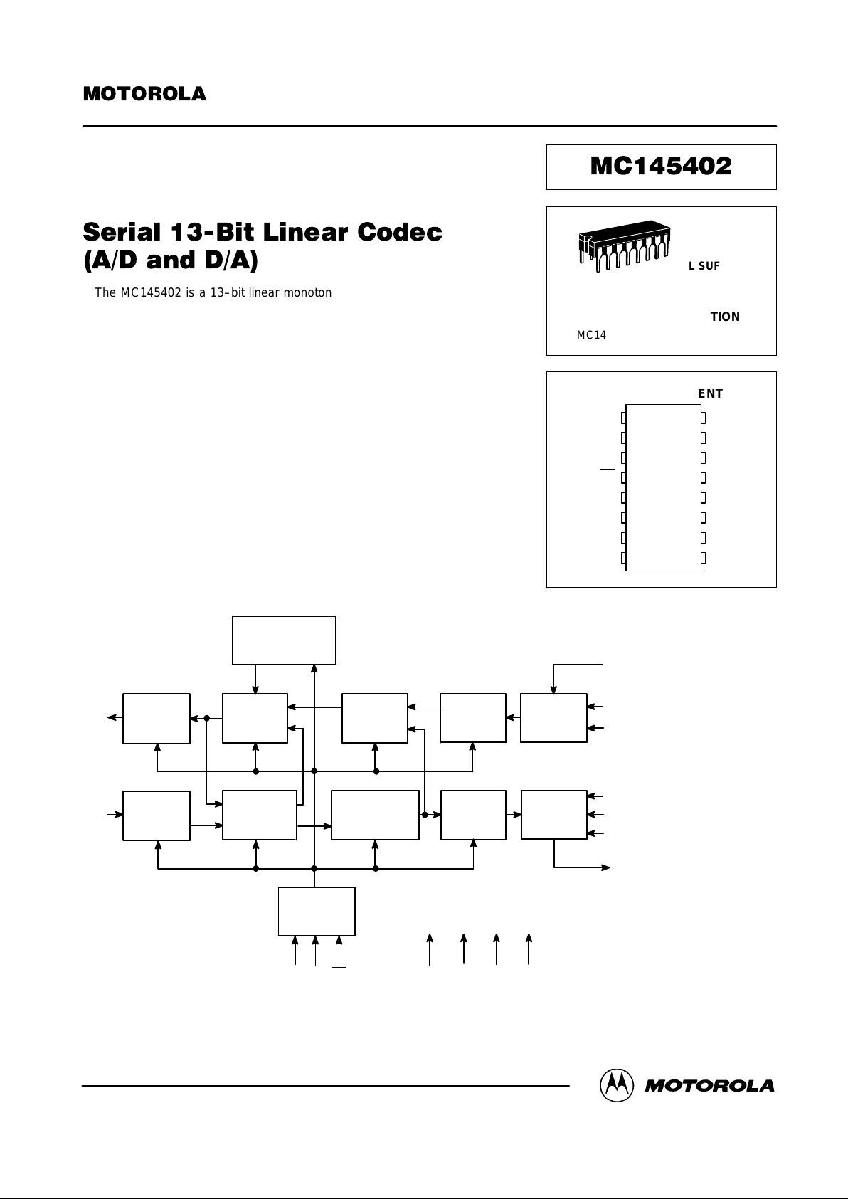
The MC145402 is a 13–bit linear monotonic digital–to–analog and analog–
to–digital converter implemented in a single silicon–gate CMOS IC. Potential
applications include analog interface for Digital Signal Processor (DSP)
applications, high speed modems, telephone systems, SONAR, Adaptive
Differential Pulse Code Modulation (ADPCM) converters, echo cancellers,
repeaters, voice synthesizers, and music synthesizers.
• 60 dB Signal–to–(Noise Plus Distortion) Ratio Typical
• On–Chip Precision Voltage Reference
• Serial Data Ports
• Two’ s Complement Coding
•± 5 V Supply Operation
• Sample Rates from 100 Hz to 16 kHz (Both A/D and D/A), 100 Hz to
21.3 kHz (A/D Only), and 100 Hz to 64 kHz (D/A Only)
• Input Sample and Hold Provided On–Chip
• 5 V CMOS Inputs; Outputs Capable of Driving Two LSTTL Loads
• Available in a 16–Pin DIP
• Low Power Consumption: 50 mW Typical, 1 mW Power–Down
BLOCK DIAGRAM
BANDGAP VOLTAGE
REFERENCE
SAMPLE
AND HOLD
D/A
CONVERTER
DATA
SELECTOR
RECEIVE
LATCH
RECEIVE
SHIFT
REGISTER
15
RDD
13
14
RDC
RCE
2
3
A
out
A
in
7
10
12
11
TDF
TDE
TDC
TDD
65 4 16 8 1 9
VDDVSSVAGV
DG
MSI CCI PDI
SEQUENCE
CONTROLLER
SAMPLE
AND HOLD
COMPARATOR/
OP AMP
SUCCESSIVE
APPROXIMA TION
REGISTER
TRANSMIT
LATCH
TRANSMIT
SHIFT
REGISTER
This document contains information on a new product. Specifications and information herein are subject to change without notice.
Order this document
by MC145402/D
SEMICONDUCTOR TECHNICAL DATA
PIN ASSIGNMENT
L SUFFIX
CERAMIC PACKAGE
CASE 620
ORDERING INFORMATION
MC145402L Ceramic Package
16
1
16
15
14
13
12
11
10
9
V
AG
A
out
A
in
PDI
CCI
MSI
TDF
V
SS
V
DD
RDD
RCE
RDC
TDC
TDE
V
DG
TDD
•
1
2
3
4
5
6
7
8
Motorola, Inc. 1995
Page 2
MC145402 MOTOROLA
2
ABSOLUTE MAXIMUM RATINGS (Voltages Referenced to V
SS
)
Rating Symbol Value Unit
DC Supply Voltage VDD – V
SS
– 0.5 to 11 V
Voltage, Any Pin to VSS V – 0.5 to VDD + 0.5 V
DC Current Drain per Pin (Excluding
VDD, VSS)
I 10 mA
Operating Temperature Range T
A
– 40 to + 85
°C
Storage Temperature Range T
stg
– 85 to + 150
°C
RECOMMENDED OPERATING CONDITIONS
Parameter Pins
0 to 70°C
Min
25°C
Typ
0 to 70°C
Max
Unit
DC Supply Voltage VDD to V
SS
9.5 10 10.5 V
Power Dissipation, PDI = 1 VDD to V
SS
— 50 80 mW
Power Dissipation, PDI = 0 VDD to V
SS
— 1 5 mW
Conversion Rate Full Cycle A/D and D/A
Short Cycle A/D
Short Cycle D/A
MSI 0.1
0.1
0.1
—
—
—
16
21.3
64
kHz
Conversion Sequence Rate CCI 3.2 — 512 kHz
Data Rate TDC, RDC 16 x f
MSI
— 4096 kHz
Full Scale Analog Levels (Referenced to 600 Ω) AI, AO —
—
3.27
9.5
—
—
Vp
dBm
DIGITAL ELECTRICAL CHARACTERISTICS (V
DD
= 5 V, VSS = – 5 V, VAG = VDG = 0 V, TA = 0 to 70°C)
Characteristic Symbol Min Max Unit
High Level Input Voltage V
IH
3.5 — V
Low Level Input Voltage V
IL
— 1.5 V
Input Current I
in
— ± 1.0 µA
Input Capacitance C
in
— 10 pF
High Level Output Voltage TDD I
out
= – 20 µA
I
out
= – 1 mA
V
OH
4.9
4.3
—
—
V
Low Level Output Voltage TDD I
out
= – 20 µA
I
out
= – 1 mA
V
OL
—
—
0.1
0.4
V
This device contains circuitry to protect the
inputs against damage due to high static
voltages or electrical fields; however, it is
advised that normal precautions be taken to
avoid applications of any voltage higher than
maximum rated voltages to this high impedance circuit. For proper operation it is recommended that Vin and V
out
be constrained to
the range VSS ≤ (Vin or V
out
) ≤ VDD on analog
inputs/outputs and VDG
≤ (V
in
or V
out
) ≤ V
DD
on digital inputs/outputs. Reliability of operation is enhanced if unused digital inputs are tied
to an appropriate logic voltage level (e.g.,
either VDG or VDD) and unused analog Inputs
are tied to VAG.
Page 3
MC145402MOTOROLA
3
CODER AND DECODER PERFORMANCE (V
DD
= 5 V ± 5%, VSS = – 5 V ± 5%, VAG = VDG = 0 V,
0 dBm0 = 1.60 Vrms = 6.30 dBm (600 Ω), TA = 0 to 70°C, MSI = TDE = RCE = 8 kHz, TDC = RDC = 2.048 MHz, CCI = 256 kHz)
Coder (A/D) Decoder (D/A)
Characteristic
Min Typ Max Min Typ Max
Unit
Resolution 13 — 13 13 — 13 Bits
Conversion Time Full Cycle A/D and D/A
Short Cycle A/D
Short Cycle D/A
62.5
46.9
—
—
—
—
10,000
10,000
—
62.5
—
15.6
—
—
—
10,000
—
10,000
µs
Differential Nonlinearity — — ± 1 — — ± 1 LSB
Gain Error – 0.35 — + 0.35 – 0.35 — + 0.35 dB
Offset – 15
—
—
—
+ 15
—
—
– 20
—
—
—
+ 20
LSB
mV
Idle Channel Noise, 3 kHz Low–Pass — – 75 — — –79 — dBm0
Signal–to–Noise 3.2 dBm0
(Referenced to 1.02 kHz through 0 dBm0
a f
MSI
/2 Low–Pass Filter) – 10 dBm0
– 20 dBm0
– 30 dBm0
– 40 dBm0
– 50 dBm0
—
—
—
—
—
—
—
61
60
57
50
40
30
20
—
—
—
—
—
—
—
—
—
—
—
—
—
—
62
60
59
52
42
32
22
—
—
—
—
—
—
—
dB
ANALOG ELECTRICAL CHARACTERISTICS (V
DD
= 5 V ± 5%, VSS = – 5 V ± 5%, VAG = VDG = 0 V,
0 dBm0 = 1.60 Vrms = 6.30 dBm (600 Ω), TA = 0 to 70°C, MSI = TDE = RCE = 8 kHz, TDC = RDC = 2.048 MHz, CCI = 256 kHz)
Characteristic Pin Symbol Min Typ Max Unit
Input Current AI I
in
— 0.01 ± 1 µA
AC Input Impedance AI Z
in
0.5 — — MΩ
Input Capacitance AI C
in
— — 15 pF
Output Voltage Range AO V
out
– 3.4 — 3.4 V
Power Supply Rejection Ratio
(100 mV RMS on VDD or VSS, 0 – 50 kHz)
AO, TDD PSRR — 40 — dB
Crosstalk, Ain to A
out
and RDD to TDD Referenced to
0 dBm0 @ 1.02 kHz
AO, TDD — — – 90 – 75 dB
Slew Rate AO SR 1.5 3 — V/µs
Settling Time (Full Scale) AO t
settle
— 8 — µs
Page 4

MC145402 MOTOROLA
4
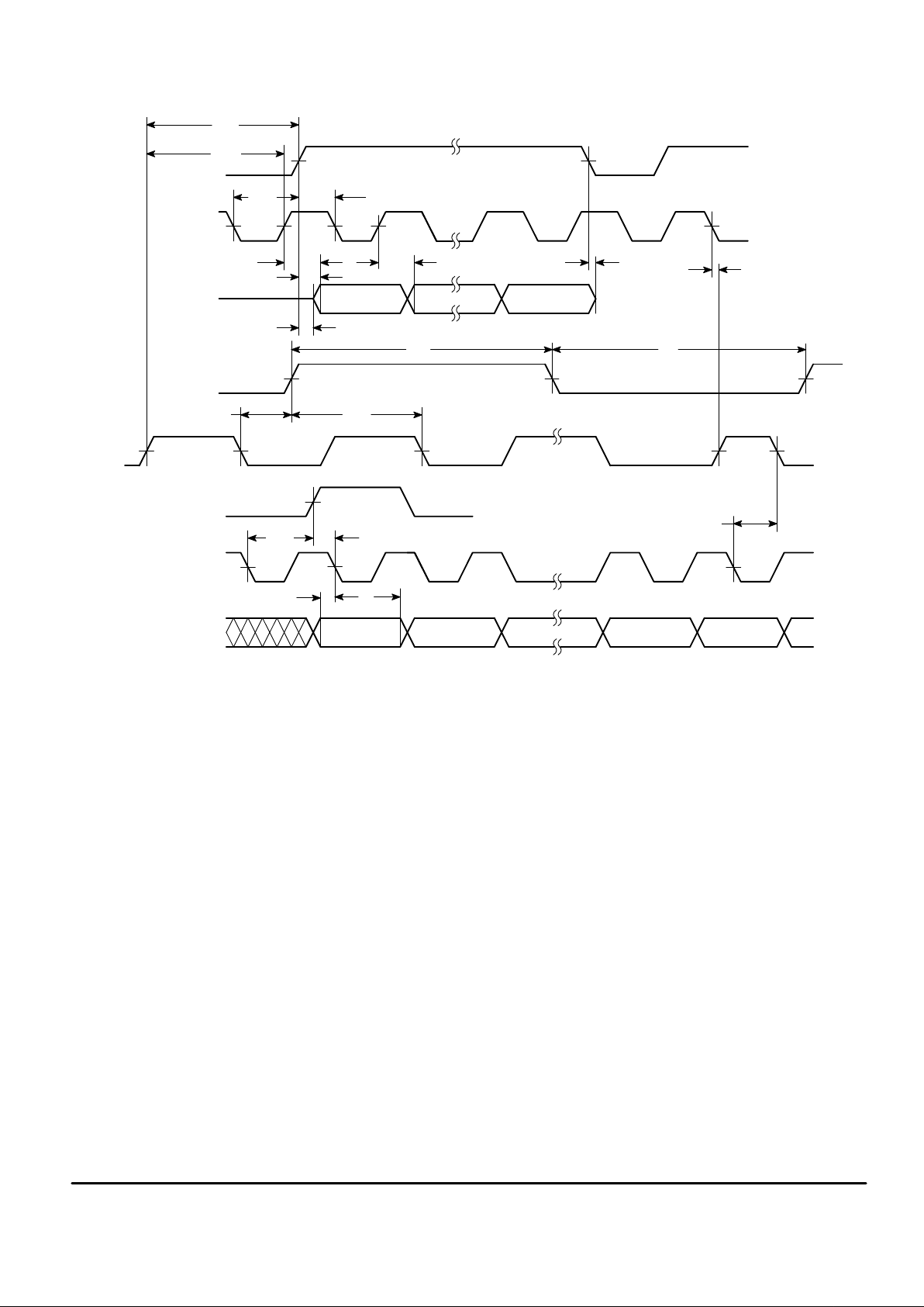
SWITCHING CHARACTERISTICS
(VDD = + 5 V ± 5%, VSS = – 5 V ± 5%, VAG = VDG = 0 V, TA = 0 to 70°C, CL = 50 pF, See Figure 1)
Characteristic Symbol Min Max Unit
Input Rise Time RCE, RDC, TDC, TDE, CCI, MSI t
r
— 100 ns
Input Fall Time RCE, RDC, TDC, TDE, CCI, MSI t
f
— 100 ns
Output Rise Time TDD t
r
— 80 ns
Output Fall Time TDD t
f
— 80 ns
Pulse Width High RDC, MSI, CCI, TDC, RCE t
wH
100 — ns
Pulse Width Low TDE, MSI, TDC, RCE, RDC t
wL
100 — ns
CCI Pulse Width Low t
wL
500 — ns
MSI Clock Frequency f
MSI
0.1 64 kHz
CCI Clock Frequency f
CCI
3.2 512 kHz
TDC and RDC Clock Frequency f
DC
16 x f
MSI
4.1 MHz
TDC Rising Edge to TDD Data Valid During TDE High t
p1
— 150 ns
TDE Rising Edge to TDD Data Valid During TDC High t
p2
— 150 ns
TDE Rising Edge to TDD Low–Impedance Propagation Delay t
p3
0 100 ns
TDE Falling Edge to TDD High–Impedance Propagation Delay t
p4
— 40 ns
TDE Rising Edge to TDC Falling Edge Setup Time t
su1
t
su2
20
100
—
—
ns
RDC Bit 0 Falling Edge to Last CCI Falling Edge Prior to MSI t
su3
20 — ns
MSI Rising Edge to CCI Falling Edge Setup Time t
su4
t
su5
20
100
—
—
ns
Last CCI Rising Edge (Prior to MSI) to TDE Rising Edge t
su6
100 — ns
Last CCI Rising Edge (Prior to MSI) to First TDC Rising Edge t
su6’
100 — ns
First TDC Falling Edge to Last CCI Rising Edge Prior to MSI t
su7
0 — ns
RCE Rising Edge to RDC Falling Edge Setup Time t
su8
t
su9
20
100
—
—
ns
RDD Valid to RDC Falling Edge Setup T ime t
su10
60 — ns
RDD Hold Time from RDC Falling Edge t
h
100 — ns
Page 5
MC145402MOTOROLA
5
t
su1
TDE
TDC
TDD
MSI
CCI
RCE
RDD
t
su6
t
su2
t
p1
t
p2
t
p1
t
p4
t
su7
t
p3
t
wH
t
wL
t
su4
t
su5
t
su8
t
su9
t
su10
t
h
t
su3
S B11 B10 B1 B0
t
su6
′
CCI
LAST
CCI
LAST
Figure 1. AC Timing Diagram
LAST
BIT
CLOCK
RDC
Page 6

MC145402 MOTOROLA
6
PIN DESCRIPTIONS
V
DD
Positive Supply (Pin 16)
The most positive power supply, typically + 5 V in split
power supply configurations, or + 10 V in single supply
systems.
V
SS
Negative Supply (Pin 8)
The most negative power supply, typically – 5 V in split
power supply configurations, or 0 V in single supply systems.
V
AG
Analog Ground (Pin 1)
This is the analog signal reference point. This pin is normally tied to 0 V in split supply operation or VDD/2 in single
supply systems.
V
DG
Digital Ground (Pin 9)
This is the ground reference for all of the digital input and
output pins. CMOS compatible logic signals swing from V
DG
to VDD where VDG can be established anywhere from VDD –
4.75 V to VSS.
A
out
Analog Output (Pin 2)
This is the output of the decoder’s sample and hold circuit
and is a 100% duty cycle analog output of the last digital
word received and decoded by the decoder. A
out
is updated
approximately 60 ns after the rising edge of the last CCI prior
to MSI (see Figure 2). A
out
is capable of driving a 10 kΩ,
50 pF load.
A
in
Analog Input (Pin 3)
This is the high–impedance input to the coder. An A/D
cycle begins on the first falling edge of CCI following the rising edge of MSI. Ain is sampled approximately 50 ns after the
rising edge of CCI prior to the start of the A/D cycle.
PDI
Power–Down Input (Pin 4)
In normal operation this Input should be tied high. A logic
low on this input puts the device into a minimum power dissipation mode. During power–down, all functions stop. Two
complete MSI conversion cycles are required to establish
normal operation after leaving the power–down mode.
CCI
Convert Clock Input (Pin 5)
This input controls the complete conversion sequence during one MSI cycle and must receive a clock which is 32 times
the frequency of MSI. The only exception to 32 times the frequency of MSI is during short–cycle operation. See General
Modes of Operation section. CCI must be synchronous and
approximately rising edge aligned with MSI.
MSI
Master Sync Input (Pin 6)
This pin determines the conversion rate for both the coder
and the decoder. One A/D and D/A conversion takes place
during each period of the digital clock applied to this input
(except in short–cycle operation, see General Modes of
Operation section). MSI must be synchronous and approximately rising edge aligned with CCI.
TDC
Transmit Data Clock (Pin 12)
Digital data from the coder is serially transmitted from TDD
on rising TDC edges whenever TDE is a logic high. TDC
must be approximately rising edge aligned with TDE. Generally, if TDC is low when TDE rises, the first rising edge of
TDC clocks the first data bit. If TDC is high when TDE rises,
the first bit will be clocked by TDE and the first rising edge of
TDC after TDE rises will clock out the second data bit.
TDE
Transmit Data Enable (Pin 10)
This pin is used to initiate the serial transfer of data from
the coder and provides three–state control of the TDD pin.
The rising edge of TDE (or TDC if it follows TDE) signals the
start of data transfer from the TDD pin. A resulting high logic
level on TDE also releases TDD from its high–impedance
state. TDE must remain high throughout the data transfer to
keep TDD in the low–impedance state and must return to a
low state prior to each data transfer. If TDE remains high for
more than 16 TDC clocks, the 16 bits of TDD data will be recirculated. (Note: The A/D cycle begins on the first falling
edge of CCI after the rising edge of MSI. The internal transmit latch is updated one and one half CCI periods prior to the
start of the A/D cycle. A pulse generated by the logical AND
of TDE and the first TDC transfers data to the transmit shift
register, and this pulse must not occur when the transmit
latch is updated. See Figure 2 and see t
su6
, t
su6′
, and t
su7
of Figure 1.
TDD
Transmit Digital Data (Pin 11)
This is the three–state output data pin from the coder and
is controlled by the TDE and TDC pins. TDD is in the high–
impedance state whenever TDE is a logic low. The first data
bit is output from TDD on the rising edge of TDE (or TDC if it
follows TDE) and each subsequent bit is output on rising
edges of TDC. Two output data formats are available as described in the TDF pin description below.
TDF
Transmit Data Format (Pin 7)
The 13–bit digital output of the coder is available in one of
two 16–bit two’s complement formats as determined by the
state of this pin. A logic 0 at this pin causes the data from
TDD to be in a 16–bit sign–extended format as follows:
SSSSM ... L where S, M, and L represent the sign, most significant bit, and the least significant bit, respectively . A logic 1
on this pin formats the data as follows: SM ... LSSS (see Figure 3). RDD data is not affected by the state of this pin and if
a “digital loopback” is needed (TDD data looped back into
RDD), this pin should be high.
Page 7

MC145402MOTOROLA
7
RDC
Receive Data Clock (Pin 13)
Receive digital data is accepted by the decoder on the first
13 falling edges of RDC after an RCE rising edge.
RCE
Receive Clock Enable (Pin 14)
This pin identifies the beginning of a data transfer into the
RDD pin of the decoder. The first 13 falling edges of RDC after an RCE rising edge will clock data into the decoder data
input, RDD. RCE must return low prior to each data transfer.
Since receive data is latched into the receive latch on the last
CCI falling edge prior to MSI, data transfers may not span
this falling edge of CCI without loss of data.
RDD
Receive Digital Data (Pin 15)
This pin is the data input to the decoder and is controlled
by the RDC and RCE pins described above. Two’s complement data are loaded in the following sequence: SM ... L
where S, M, and L represent the sign, most significant bit,
and the least significant bit, respectively. Only the first 13 bits
clocked by RDC after RCE rises will be accepted for decoding. Any additional bits will be ignored (see Figure 3).
GENERAL INFORMATION
GENERAL MODES OF OPERATION
The MC145402 has three modes of operation; a “full” cycle
mode and two ‘‘short” cycle modes. The full cycle mode allows simultaneous analog–to–digital (A/D) and digital–to–
analog (D/A) operation. The short cycle modes allow either
A/D only or D/A only operation. Two MSI cycles are required
for the MC145402 to detect which operating mode has been
selected. See Figure 2 for full versus short cycle clocking.
Full Cycle Operation
When operating in the full cycle mode, the MC145402 performs a 13–bit A/D conversion followed by a 13–bit D/A con–
version. Full cycle operation is selected by using a CCI
frequency that is 32 times the frequency of MSI. MSI is the
sample rate frequency.
Short Cycle Analog–to–Digital Operation
If CCI is 24 times the frequency of MSI, short cycle analog–to–digital operation is selected. This allows a 13–bit A/D
conversion only. In this mode, the D/A is not operational and
any data applied to the RDD input is ignored.
Short Cycle Digital–to–Analog Operation
Short cycle digital–to–analog operation is selected by
using a CCI clock frequency that is eight times the MSI sample rate. During short cycle D/A operation, A/D operation is
disabled and digital data read from TDD is not valid.
CLOCKING RECOMMENDATIONS
For optimum differential nonlinearity performance, all data
transitions on TDD and RDD should be limited to the first four
CCI cycles following the rising edge of MSI. This may be
achieved by setting MSI = TDE = RCE having a duration of
16 da ta clo ck cy cles , and TD C = RDC
≥ 4 x CCI c lock
frequency. Figure 6 shows a circuit that generates this clocking configuration; see Application Circuits section.
SIGNAL TO DISTORTION RATIO
Figures 4 and 5 show graphs of typical signal to distortion
ratios versus signal level for the MC145402. The presented
data is referenced to a 1020 Hz input sinusoidal frequency
with signal levels referenced to 600 Ω and transmission level
point adjusted (e.g., 0 dBm0 at 600 Ω with a TLP of 6.30 dB
is 4.53 V peak–to–peak). For comparison, ideal signal to
noise ratios for 9–, 10–, 11–, 12–, and 13–bit A/D and D/A
converters are also shown. The equation used for an ideal
RMS to RMS signal to distortion ratio is:
S/D = N x 6 dB + 1.76 dB
where N is the number of bits of resolution, 6 dB per bit, and
1.76 = 20
log
(√3
/√2).
(√3
/√2) is approximately the RMS to RMS ratio of a sine
wave to white noise.
The signal to noise plus distortion ratio is measured
through a brickwall low–pass filter set to the Nyquist frequency of the A/D and D/A sample rate. For an 8 kHz sample rate,
the low–pass filter is set to block all signals above 4 kHz.
APPLICATION CIRCUITS
Figure 6 shows a typical circuit for generating the clock
frequencies for the MC145402. This circuit uses an
MC74HC4040 and a 2.048 MHz crystal to generate the
256 kHz frequency for internal sequencing, 1.024 MHz for
the date clocks, and an 8 kHz sample frequency. A
4.096 MHz crystal could be used for a sample rate of 16 kHz.
Figure NO TAG shows the MC145402 interfaced to the
DSP56000 digital signal processor. The DSP56000 can internally generate the clocks for the MC145402 using the SSI
serial interface. SCK provides the sequencing and data
clocks (non–gated continuous dock) and SC2 (setup as the
Frame Sync Out, FSL = 0) provides the sample rate and data
enables for the MC145402. The divide–by–four circuit to
generate the CCI clock is recommended for optimum
MC145402 performance, and allows the DSP56000 to clock
data in and out of the MC145402 quickly, leaving time available for processing by the DSP before another sample is
available. SC0 and SC1 could be used to gate the enables to
select up to four devices on the SSI bus.
TELEPHONE SYSTEM TRANSMISSION LEVEL POINT
FOR A LINEAR A/D OR D/A CONVERTER
REFERENCED TO MU–LAW COMPANDING
Mu–Law companding, as specified by AT&T and CCITT,
requires 8159 quantization levels to implement both A/D and
D/A conversion schemes. This is to be mirrored about signal
ground for the negative part of the wave form.
To implement a 13–bit (± 12–bit) linear converter scheme
requires 8192 quantization levels mirrored about signal
ground. To specify this converter such that it can be used to
interface with, or as an alternative to, telephony based Mu–
Law applications, the following is an explanation of the gain
translation.
A 13–bit linear converter scheme has 8192 quantization
levels. The goal is to be able to convert between these two
encoding schemes with minimal distortion. This dictates setting the LSBs to the same level. For this to be achieved requires the reference voltage of the linear converter to be
Page 8

MC145402 MOTOROLA
8
8192/8159 times the reference voltage of the Mu–Law
converter. The peak amplitude of a Mu–Law converter is
3.17 dBm0. The peak level of the linear converter will be
8192/8159 times the peak level of the Mu–Law converter,
which is 8192/8159 x 3.17 dBm0. However, you cannot multiply a gain factor by a dBm value without using common term
units and math (i.e., we must convert this gain factor to a dB
equivalent), which is:
20 log10 (8192/8159) = 0.03 dB
With the gain factor in dB, we can add it to the Mu–Law
peak level:
3.17 dBm0 + 0.03 dB = 3.20 dBm0
Therefore, the linear converter peak level is 3.20 dBm0.
This is another way of saying the 0 dBm0 level for the linear converter is 3.20 dB below the maximum amplitude.
To determine the absolute 0 dBm0 level for the linear converter from the peak level, we calculate the peak level in dBm
by:
10 log
10
3.27 VpK
/√2 )/(600 Ω)
1 mW
= 9.50 dBm (600 Ω)
and 3.20 dB below this level is the 0 dBm0 absolute amplitude, which is
9.50 dBm – 3.20 dB = 6.30 dBm (600 Ω)
Therefore, the calibration level, or transmission level point
(TLP), for this part is 6.30 dBm (600 Ω), which is 1.6 Vrms
based on the reference voltage of 3.27 V.
Page 9

MC145402MOTOROLA
9
AO UPDATED AND
FULL CYCLE A/D–D/A
SHORT CYCLE A/D ONLY
SHORT CYCLE D/A ONLY
A/D CONVERSION
A/D CONVERSION A/D CONVERSION
AI SAMPLED
AI SAMPLED
AO UPDATED
1 8 16 24 32
MSI
MSI
MSI
CCI
CCI
CCI
TDD DATA TRANSFERRED INT O
D/A
CONVERSION
D/A
CONVERSION
D/A
CONVERSION
D/A
CONVERSION
D/A
CONVERSION
RDD DATA LATCHED INTO
THE RECEIVE LATCH
RDD DATA LATCHED INTO
THE RECEIVE LATCH
THE TRANSMIT LATCH
TDD DATA TRANSFERRED
INTO THE TRANSMIT LA TCH
CLOCK
CYCLE
Figure 2. MC145402 Full and Short Cycle Timing
Page 10

MC145402 MOTOROLA
10
TDE
TDC
RCE
RDC
RDD
TDD
(TDF = 1)
TDD
(TDF = 0)
S
S
SS
S
SSSS b0b9b11 b10 b8 b7 b6 b5 b4 b3 b2 b1
b0b9b11 b10 b8 b7 b6 b5 b4 b3 b2 b1
b0b9b11 b10 b8 b7 b6 b5 b4 b3 b2 b1
Figure 3. MC145402 Digital Data Timing
Page 11

MC145402MOTOROLA
11
(1020 Hz REFERENCED TO 600
INPUT LEVEL (dBm0)
Ω
)
80
70
60
50
40
30
20
10
0
– 60 – 50 – 40 – 30 – 20 – 10 0 10
13–BIT
12–BIT
11–BIT
10–BIT
9–BIT
RMS SIGNAL TO RMS (NOISE + DIST ORTION) (dB)
f
MSI
/2
COMPARED TO 9–13 BIT IDEAL A/D; MSI = 8 kHz;
MEASURED THROUGH A LOW–P ASS FIL TER
WITH A BANDWIDTH OF
Figure 4. MC145402 Encoder (A/D) Signal to Noise Plus Distortion Ratio
(1020 Hz REFERENCED TO 600
INPUT LEVEL (dBm0)
Ω
)
80
70
60
50
40
30
20
10
0
– 60 – 50 – 40 – 30 – 20 – 10 0 10
13–BIT
12–BIT
11–BIT
10–BIT
9–BIT
RMS SIGNAL TO RMS (NOISE + DIST ORTION) (dB)
f
MSI
/2
COMPARED TO 9–13 BIT IDEAL D/A; MSI = 8 kHz;
MEASURED THROUGH A LOW–P ASS FIL TER
WITH A BANDWIDTH OF
Figure 5. MC145402 Decoder (D/A) Signal to Noise Plus Distortion Ratio
Page 12

MC145402 MOTOROLA
12
A/D
2.048 MHz
15 M
20 pF 20 pF
MC74HCU04
+ 5 V
0 V
V
DD
V
CC
16
10
8
CLK
GND
R
9
6
2
4
13
Q1
Q2
Q3
Q4
Q5
Q6
Q7
Q8
Q9
Q10
Q11
Q12
V
SS
V
DG
15
13
14
7
11
12
10
5
6
4
+ 5 V
8 kHz
256 kHz
+ 5 V
MC145402
CONTROL
2
3
16
8
9
1
out
RDD
RDC
RCE
TDF
TDD
TDC
TDE
CCI
MIS
PDI
+ 5 V
–5 V
0 V
µ
F0.1
µ
F0.1
V
CC
GND, PIN 7 = 0 V
, PIN 14 = + 5 V
13–BIT
POWER CONNECTIONS
MC74HCU04 AND MC74HC11
MC74HC1 1
1/3
MHz
1.024
DAT A
SERIAL
IN
DAT A
SERIAL
OUT
VOLT AGE
ANALOG
OUT
VOLT AGE
ANALOG
IN
D/A
13–BIT
11
MC74HC4040
V
AG
A
in
A
Ω
Figure 6. Typical MC145402 Configuration
Page 13

MC145402MOTOROLA
13
+ 5 V
128 f
sample
32 f
samplefsample
+ 5 V
+ 5 V
+ 5 V
V
CC
V
SS
256
kHz
1.024
MHz
8 kHz
DSP56000
1/2 MC74HC74
1/2 MC74HC73
1/2 MC74HC731/2 MC74HC74
SCK
SC2
SRD
STD
PDI
A
in
A
out
TDF
V
AG
V
DG
CCI
TDC
RDC
TDE
RCE
MSI
TDD
RDD
CLK
CLK
CLK
CLK
D
D
R
R R
R
J
J
K
K
Q
Q
Q
Q
Q
Q Q
Q
V
out
V
in
V
SS
V
DD
MC145402
– 5 V
Figure 7. The MC145402, 13–Bit Linear Codec, Interfaced to a Motorola DSP56000,
Digital Signal Processor, SSI Port
Page 14

MC145402 MOTOROLA
14
P ACKAGE DIMENSIONS
L SUFFIX
CERAMIC
CASE 620–09
MIN MINMAX MAX
INCHES MILLIMETERS
DIM
19.05
6.10
—
0.39
1.40
0.23
—
0
°
0.39
19.55
7.36
4.19
0.53
1.77
0.27
5.08
15
°
0.88
0.750
0.240
—
0.015
0.055
0.009
—
0
°
0.015
0.770
0.290
0.165
0.021
0.070
0.011
0.200
15
°
0.035
1.27 BSC
2.54 BSC
7.62 BSC
0.050 BSC
0.100 BSC
0.300 BSC
A
B
C
D
E
F
G
J
K
L
M
N
NOTES:
1. DIMENSIONING AND TOLERANCING PER ANSI
Y14.5M, 1982.
2. CONTROLLING DIMENSION: INCH.
3. DIMENSION L TO CENTER OF LEAD WHEN
FORMED PARALLEL.
4. DIMENSION F MAY NARROW TO 0.76 (0.030)
WHERE THE LEAD ENTERS THE CERAMIC
BODY.
D 16 PL
J 16 PL
SEATING
PLANE
0.25 (0.010) T A
M
S
0.25 (0.010) T B
M
S
18
916
-A-
-B-
K
C
N
G
E
F
-T-
M
L
Page 15

MC145402MOTOROLA
15
This page intentionally left blank.
Page 16

MC145402 MOTOROLA
16
Motorola reserves the right to make changes without further notice to any products herein. Motorola makes no warranty , representation or guarantee regarding
the suitability of its products for any particular purpose, nor does Motorola assume any liability arising out of the application or use of any product or circuit,
and specifically disclaims any and all liability, including without limitation consequential or incidental damages. “T ypical” parameters can and do vary in different
applications. All operating parameters, including “T ypicals” must be validated for each customer application by customer’s technical experts. Motorola does
not convey any license under its patent rights nor the rights of others. Motorola products are not designed, intended, or authorized for use as components in
systems intended for surgical implant into the body, or other applications intended to support or sustain life, or for any other application in which the failure of
the Motorola product could create a situation where personal injury or death may occur. Should Buyer purchase or use Motorola products for any such
unintended or unauthorized application, Buyer shall indemnify and hold Motorola and its officers, employees, subsidiaries, affiliates, and distributors harmless
against all claims, costs, damages, and expenses, and reasonable attorney fees arising out of, directly or indirectly, any claim of personal injury or death
associated with such unintended or unauthorized use, even if such claim alleges that Motorola was negligent regarding the design or manufacture of the part.
Motorola and are registered trademarks of Motorola, Inc. Motorola, Inc. is an Equal Opportunity/Affirmative Action Employer.
How to reach us:
USA/EUROPE: Motorola Literature Distribution; JAPAN: Nippon Motorola Ltd.; Tatsumi–SPD–JLDC, Toshikatsu Otsuki,
P.O. Box 20912; Phoenix, Arizona 85036. 1–800–441–2447 6F Seibu–Butsuryu–Center, 3–14–2 Tatsumi Koto–Ku, To kyo 135, Japan. 03–3521–8315
MFAX: RMF AX0@email.sps.mot.com – T OUCHTONE (602) 244–6609 HONG KONG: Motorola Semiconductors H.K. Ltd.; 8B Tai Ping Industrial Park,
INTERNET: http://Design–NET.com 51 Ting Kok Road, Tai Po, N.T., Hong Kong. 852–26629298
MC145402/D
*MC145402/D*
◊
 Loading...