

Page 1
MOTOROLA CMOS LOGIC DATA
1
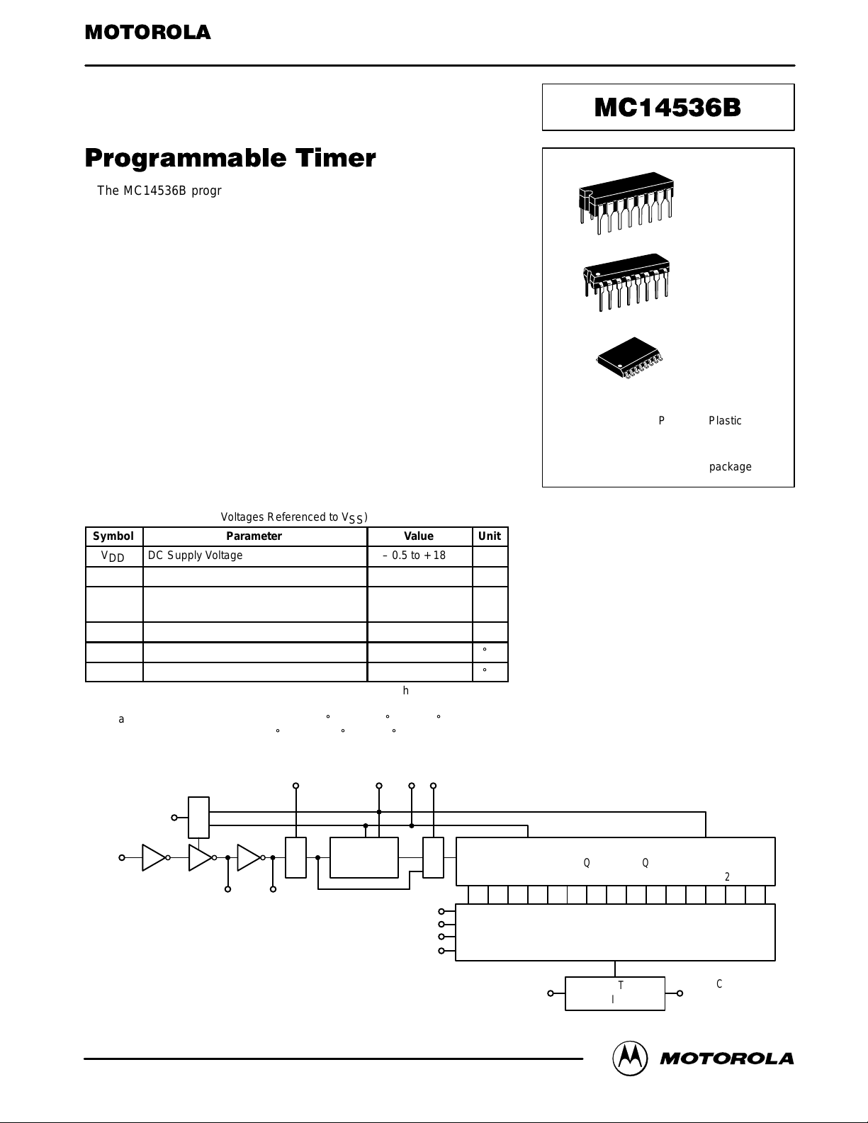
MC14536B
The MC14536B programmable timer is a 24–stage binary ripple counter
with 16 stages selectable by a binary code. Provisions for an on–chip RC
oscillator or an external clock are provided. An on–chip monostable circuit
incorporating a pulse–type output has been included. By selecting the
appropriate counter stage in conjunction with the appropriate input clock
frequency, a variety of timing can be achieved.
• 24 Flip–Flop Stages — Will Count From 20 to 2
24
• Last 16 Stages Selectable By Four–Bit Select Code
• 8–Bypass Input Allows Bypassing of First Eight Stages
• Set and Reset Inputs
• Clock Inhibit and Oscillator Inhibit Inputs
• On–Chip RC Oscillator Provisions
• On–Chip Monostable Output Provisions
• Clock Conditioning Circuit Permits Operation With Very Long Rise and
Fall Times
• Test Mode Allows Fast Test Sequence
• Supply Voltage Range = 3.0 Vdc to 18 Vdc
• Capable of Driving Two Low–power TTL Loads or One Low–power
Schottky TTL Load Over the Rated Temperature Range
MAXIMUM RATINGS* (Voltages Referenced to V
SS
)
Symbol
Parameter Value Unit
V
DD
DC Supply Voltage – 0.5 to + 18.0 V
Vin, V
out
Input or Output Voltage (DC or Transient) – 0.5 to VDD + 0.5 V
Iin, I
out
Input or Output Current (DC or Transient),
per Pin
± 10 mA
P
D
Power Dissipation, per Package† 500 mW
T
stg
Storage Temperature – 65 to + 150
_
C
T
L
Lead Temperature (8–Second Soldering) 260
_
C
*Maximum Ratings are those values beyond which damage to the device may occur.
†Temperature Derating:
Plastic “P and D/DW” Packages: – 7.0 mW/_C From 65_C To 125_C
Ceramic “L” Packages: – 12 mW/_C From 100_C To 125_C
BLOCK DIAGRAM
STAGES 9 THRU 24
Q
24
Q
23
Q22Q
21
Q20Q
19
Q18Q
17
Q16Q
15
Q14Q
13
Q12Q
11
Q10Q
9
DECODER
MONOSTABLE
MULTIVIBRATOR
DECODE
OUT
13MONO–IN 15
D 12
C 11
B 10
A 9
VDD = PIN 16
VSS = PIN 8
STAGES
1 THRU 8
8 BYPASSSETRESETCLOCK INH.
7 2 1 6
5
OUT
2
4
OUT
1
3
IN
1
OSC. INHIBIT 14
SEMICONDUCTOR TECHNICAL DATA
Motorola, Inc. 1995
REV 3
1/94
L SUFFIX
CERAMIC
CASE 620
ORDERING INFORMATION
MC14XXXBCP Plastic
MC14XXXBCL Ceramic
MC14XXXBDW SOIC
TA = – 55° to 125°C for all packages.
P SUFFIX
PLASTIC
CASE 648
DW SUFFIX
SOIC
CASE 751G
Page 2
MOTOROLA CMOS LOGIC DATAMC14536B
2
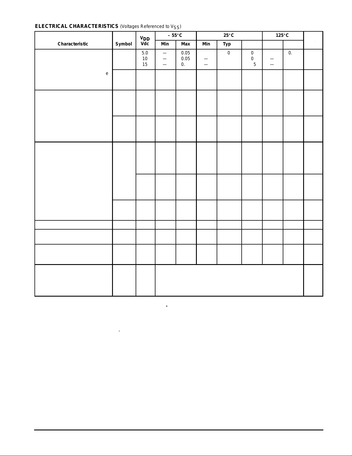
ELECTRICAL CHARACTERISTICS (Voltages Referenced to V
SS
)
V
– 55_C 25_C 125_C
Characteristic
Symbol
V
DD
Vdc
Min Max Min Typ # Max Min Max
Unit
Output Voltage “0” Level
Vin = VDD or 0
V
OL
5.0
10
15
—
—
—
0.05
0.05
0.05
—
—
—
0
0
0
0.05
0.05
0.05
—
—
—
0.05
0.05
0.05
Vdc
“1” Level
Vin = 0 or V
DD
V
OH
5.0
10
15
4.95
9.95
14.95
—
—
—
4.95
9.95
14.95
5.0
10
15
—
—
—
4.95
9.95
14.95
—
—
—
Vdc
Input Voltage “0” Level
(VO = 4.5 or 0.5 Vdc)
(VO = 9.0 or 1.0 Vdc)
(VO = 13.5 or 1.5 Vdc)
V
IL
5.0
10
15
—
—
—
1.5
3.0
4.0
—
—
—
2.25
4.50
6.75
1.5
3.0
4.0
—
—
—
1.5
3.0
4.0
Vdc
“1” Level
(VO = 0.5 or 4.5 Vdc)
(VO = 1.0 or 9.0 Vdc)
(VO = 1.5 or 13.5 Vdc)
V
IH
5.0
10
15
3.5
7.0
11
—
—
—
3.5
7.0
11
2.75
5.50
8.25
—
—
—
3.5
7.0
11
—
—
—
Vdc
Output Drive Current
(VOH = 2.5 Vdc) Source
(VOH = 4.6 Vdc) Pins 4 & 5
(VOH = 9.5 Vdc)
(VOH = 13.5 Vdc)
5.0
5.0
10
15
– 1.2
– 0.25
– 0.62
– 1.8
—
—
—
—
– 1.0
– 0.25
– 0.5
– 1.5
– 1.7
– 0.36
– 0.9
– 3.5
—
—
—
—
– 0.7
– 0.14
– 0.35
– 1.1
—
—
—
—
mAdc
(VOH = 2.5 Vdc) Source
(VOH = 4.6 Vdc) Pin 13
(VOH = 9.5 Vdc)
(VOH = 13.5 Vdc)
5.0
5.0
10
15
– 3.0
– 0.64
– 1.6
– 4.2
—
—
—
—
– 2.4
– 0.51
– 1.3
– 3.4
– 4.2
– 0.88
– 2.25
– 8.8
—
—
—
—
– 1.7
– 0.36
– 0.9
– 2.4
—
—
—
—
mAdc
(VOL = 0.4 Vdc) Sink
(VOL = 0.5 Vdc)
(VOL = 1.5 Vdc)
I
OL
5.0
10
15
0.64
1.6
4.2
—
—
—
0.51
1.3
3.4
0.88
2.25
8.8
—
—
—
0.36
0.9
2.4
—
—
—
mAdc
Input Current I
in
15 — ±0.1 — ±0.00001 ±0.1 — ±1.0 µAdc
Input Capacitance
(Vin = 0)
C
in
— — — — 5.0 7.5 — — pF
Quiescent Current
(Per Package)
I
DD
5.0
10
15
—
—
—
5.0
10
20
—
—
—
0.010
0.020
0.030
5.0
10
20
—
—
—
150
300
600
µAdc
Total Supply Current**†
(Dynamic plus Quiescent,
Per Package)
(CL = 50 pF on all outputs, all
buffers switching)
I
T
5.0
10
15
IT = (1.50 µA/kHz) f + I
DD
IT = (2.30 µA/kHz) f + I
DD
IT = (3.55 µA/kHz) f + I
DD
µAdc
#Data labelled “Typ” is not to be used for design purposes but is intended as an indication of the IC’s potential performance.
**The formulas given are for the typical characteristics only at 25_C.
†To calculate total supply current at loads other than 50 pF:
IT(CL) = IT(50 pF) + (CL – 50) Vfk
where: IT is in µA (per package), CL in pF, V = (VDD – VSS) in volts, f in kHz is input frequency, and k = 0.003.
I
OH
Page 3
MOTOROLA CMOS LOGIC DATA
3
MC14536B
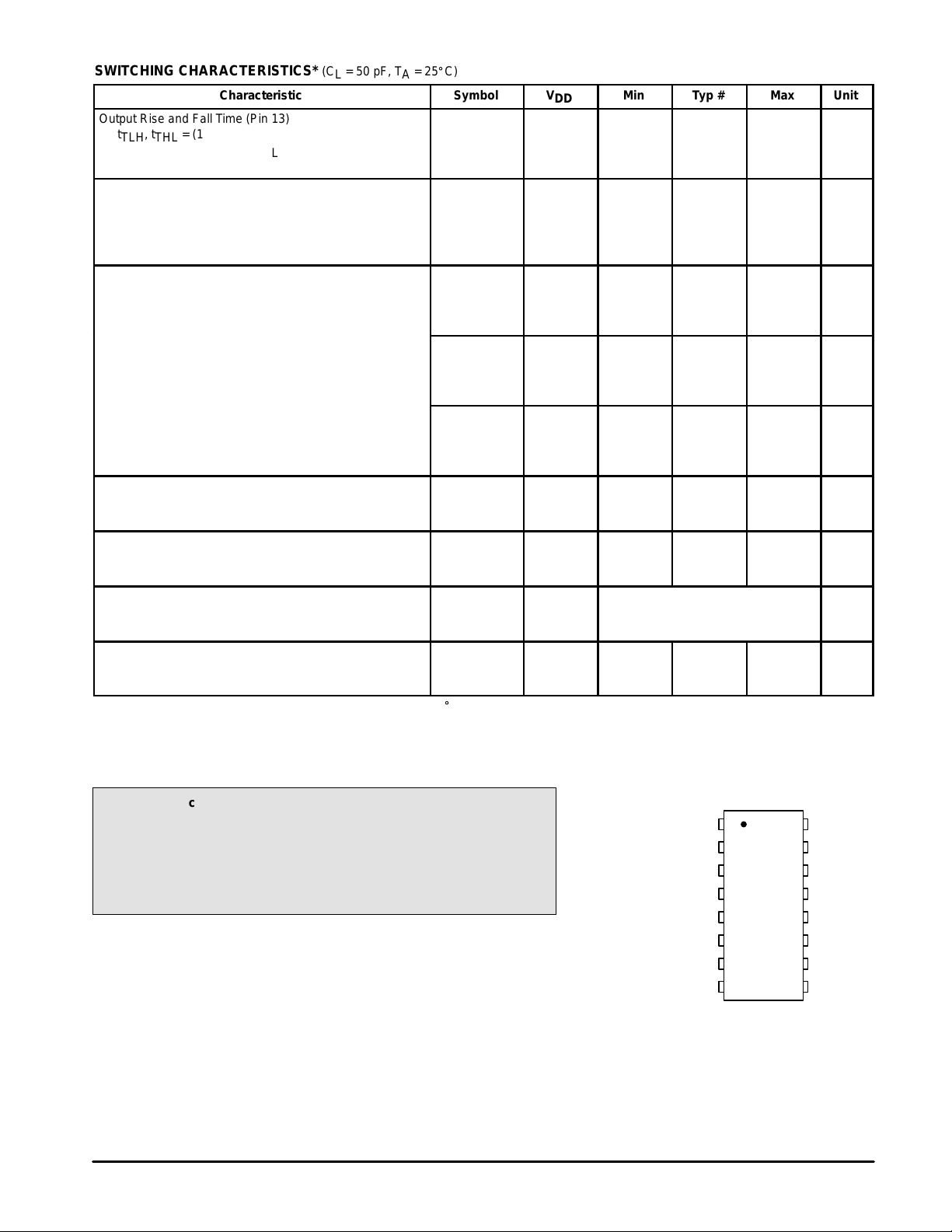
SWITCHING CHARACTERISTICS* (C
L
= 50 pF, TA = 25_C)
Characteristic
Symbol V
DD
Min Typ # Max Unit
Output Rise and Fall Time (Pin 13)
t
TLH
, t
THL
= (1.5 ns/pF) CL + 25 ns
t
TLH
, t
THL
= (0.75 ns/pF) CL + 12.5 ns
t
TLH
, t
THL
= (0.55 ns/pF) CL + 9.5 ns
t
TLH
,
t
THL
5.0
10
15
—
—
—
100
50
40
200
100
80
ns
Propagation Delay Time
Clock to Q1, 8–Bypass (Pin 6) High
t
PLH
, t
PHL
= (1.7 ns/pF) CL + 1715 ns
t
PLH
, t
PHL
= (0.66 ns/pF) CL + 617 ns
t
PLH
, t
PHL
= (0.5 ns/pF) CL + 425 ns
t
PLH
,
t
PHL
5.0
10
15
—
—
—
1800
650
450
3600
1300
1000
ns
Clock to Q1, 8–Bypass (Pin 6) Low
t
PLH
, t
PHL
= (1.7 ns/pF) CL + 3715 ns
t
PLH
, t
PHL
= (0.66 ns/pF) CL + 1467 ns
t
PLH
, t
PHL
= (0.5 ns/pF) CL + 1075 ns
t
PLH
,
t
PHL
5.0
10
15
—
—
—
3.8
1.5
1.1
7.6
3.0
2.3
µs
Clock to Q16
t
PHL
, t
PLH
= (1.7 ns/pF) CL + 6915 ns
t
PHL
, t
PLH
= (0.66 ns/pF) CL + 2967 ns
t
PHL
, t
PLH
= (0.5 ns/pF) CL + 2175 ns
t
PLH
,
t
PHL
5.0
10
15
—
—
—
7.0
3.0
2.2
14
6.0
4.5
µs
Reset to Q
n
t
PHL
= (1.7 ns/pF) CL + 1415 ns
t
PHL
= (0.66 ns/pF) CL + 567 ns
t
PHL
= (0.5 ns/pF) CL + 425 ns
t
PHL
5.0
10
15
—
—
—
1500
600
450
3000
1200
900
ns
Clock Pulse Width t
WH
5.0
10
15
600
200
170
300
100
85
—
—
—
ns
Clock Pulse Frequency
(50% Duty Cycle)
f
cl
5.0
10
15
—
—
—
1.2
3.0
5.0
0.4
1.5
2.0
MHz
Clock Rise and Fall Time t
TLH
,
t
THL
5.0
10
15
No Limit
—
Reset Pulse Width t
WH
5.0
10
15
1000
400
300
500
200
150
—
—
—
ns
*The formulas given are for the typical characteristics only at 25_C.
#Data labelled “Typ” is not to be used for design purposes but is intended as an indication of the IC’s potential performance.
This device contains protection circuitry to guard against damage
due to high static voltages or electric fields. However, precautions must
be taken to avoid applications of any voltage higher than maximum rated
voltages to this high-impedance circuit. For proper operation, Vin and
V
out
should be constrained to the range VSS ≤ (Vin or V
out
) ≤ VDD.
Unused inputs must always be tied to an appropriate logic voltage
level (e.g., either VSS or VDD). Unused outputs must be left open.
PIN ASSIGNMENT
13
14
15
16
9
10
11
125
4
3
2
1
8
7
6
D
DECODE
OSC INH
MONO IN
V
DD
A
B
C
OUT 1
IN 1
RESET
SET
V
SS
CLOCK INH
8–BYPASS
OUT 2
Page 4

MOTOROLA CMOS LOGIC DATAMC14536B
4
PIN DESCRIPTIONS
INPUTS
SET (Pin 1) — A h igh on S et asynchronously forces
Decode Out to a high level. This is accomplished by setting
an output conditioning latch to a high level while at the same
time resetting the 24 flip–flop stages. After Set goes low
(inactive), the occurrence of the first negative clock transition
on IN1 causes Decode Out to go low. The counter’s flip–flop
stages begin counting on the second negative clock transition of IN1. When Set is high, the on–chip RC oscillator is
disabled. This allows for very low–power standby operation.
RESET (Pin 2) — A high on Reset asynchronously forces
Decode Out to a low level; all 24 flip–flop stages are also
reset to a low level. Like the Set input, Reset disables the
on–chip RC oscillator for standby operation.
IN1 (Pin 3) — The device’s internal counters advance on
the negative–going edge of this input. IN1 may be used as an
external clock input or used in conjunction with OUT1 and
OUT2 to form an RC oscillator. When an external clock is
used, both OUT1 and OUT2 may be left unconnected or
used to drive 1 LSTTL or several CMOS loads.
8–BYPASS (Pin 6) — A high on this input causes the first
8 flip–flop stages to be bypassed. This device essentially becomes a 16–stage counter with all 16 stages selectable.
Selection is accomplished by the A, B, C, and D inputs. (See
the truth tables.)
CLOCK INHIBIT (Pin 7) — A high on this input disconnects the first counter stage from the clocking source. This
holds the present count and inhibits further counting. However, the clocking source may continue to run. Therefore,
when Clock Inhibit is brought low, no oscillator start–up time
is required. When Clock Inhibit is low, the counter will start
counting on the occurrence of the first negative edge of the
clocking source at IN1.
OSC INHIBIT (Pin 14) — A high level on this pin stops the
RC oscillator which allows for very low–power standby operation. May also be used, in conjunction with an external
clock, with essentially the same results as the Clock Inhibit
input.
MONO–IN (Pin 15) — Used as the timing pin for the on–
chip monostable multivibrator. If the Mono–In input is connected to VSS, the m onostable circuit is d isabled, a nd
Decode Out is directly connected to the selected Q output.
The monostable circuit is enabled if a resistor is connected
between Mono–In and VDD. This resistor and the device’s internal capacitance will determine the minimum output pulse
widths. With the addition of an external capacitor to VSS, the
pulse width range may be extended. For reliable operation
the resistor value should be limited to the range of 5 kΩ to
100 kΩ and the capacitor value should be limited to a maximum of 1000 pf. (See figures 3, 4, 5, and 10).
A, B, C, D (Pins 9, 10, 11, 12) — These inputs select the
flip–flop stage to be connected to Decode Out. (See the truth
tables.)
OUTPUTS
OUT1, OUT2 (Pin 4, 5) — Outputs used in conjunction with
IN1 to form an RC oscillator. These outputs are buffered and
may be used for 20 frequency division of an external clock.
DECODE OUT (Pin 13) — Output function depends on
configuration. When the monostable circuit is disabled, this
output is a 50% duty cycle square wave during free run.
TEST MODE
The test mode configuration divides the 24 flip–flop stages
into three 8–stage sections to facilitate a fast test sequence.
The test mode is enabled when 8–Bypass, Set and Reset
are at a high level. (See Figure 8.)
Page 5

MOTOROLA CMOS LOGIC DATA
5
MC14536B
TRUTH TABLES
Input
Stage Selected
8–Bypass D C B A
Stage Selected
for Decode Out
0 0 0 0 0 9
0 0 0 0 1 10
0 0 0 1 0 11
0 0 0 1 1 12
0 0 1 0 0 13
0 0 1 0 1 14
0 0 1 1 0 15
0 0 1 1 1 16
0 1 0 0 0 17
0 1 0 0 1 18
0 1 0 1 0 19
0 1 0 1 1 20
0 1 1 0 0 21
0 1 1 0 1 22
0 1 1 1 0 23
0 1 1 1 1 24
Input
Stage Selected
8–Bypass D C B A
Stage Selected
for Decode Out
1 0 0 0 0 1
1 0 0 0 1 2
1 0 0 1 0 3
1 0 0 1 1 4
1 0 1 0 0 5
1 0 1 0 1 6
1 0 1 1 0 7
1 0 1 1 1 8
1 1 0 0 0 9
1 1 0 0 1 10
1 1 0 1 0 11
1 1 0 1 1 12
1 1 1 0 0 13
1 1 1 0 1 14
1 1 1 1 0 15
1 1 1 1 1 16
FUNCTION TABLE
In
1
Set Reset
Clock
Inh
OSC
Inh
Out 1 Out 2
Decode
Out
0 0 0 0 No
Change
0 0 0 0 Advance to
next state
X 1 0 0 0 0 1 1
X 0 1 0 0 0 1 0
X 0 0 1 0 — — No
Change
X 0 0 0 1 0 1 No
Change
0 0 0 0 X 0 1 No
Change
1 0 0 0 Advance to
next state
X = Don’t Care
Page 6

MOTOROLA CMOS LOGIC DATAMC14536B
6
LOGIC DIAGRAM
STAGES
18 THRU
23
2417
STAGES
10 THRU
15
16
T
9
STAGES
2 THRU 7
8
T
1
6
2
RESET
8–BYPASS
14
OSC INHIBIT
3
IN
1
4
OUT 1
OUT 2 5
SET
1
7
CLOCK
INHIBIT
R
En
C
S
Q
A 9
B 10
C 11
D 12
DECODER
DECODER
OUT
13
15
MONO–IN
V
DD
= PIN 16
V
SS
= PIN 8
Page 7

MOTOROLA CMOS LOGIC DATA
7
MC14536B
Figure 1. RC Oscillator Stability Figure 2. RC Oscillator Frequency as a
Function of RTC and C
RS = 0, f = 10.15 kHz @ VDD = 10 V, TA = 25°C
RS = 120 kΩ, f = 7.8 kHz @ VDD = 10 V, TA = 25°C
RTC = 56 k
Ω
,
C = 1000 pF
VDD = 15 V
10 V
5.0 V
8.0
4.0
0
–4.0
–8.0
–12
–16
–55 –25 0 25 50 75 100 125
TA, AMBIENT TEMPERATURE (
°
C)*
*Device Only.
FREQUENCY DEVIATION (%)
TYPICAL RC OSCILLATOR CHARACTERISTICS
(For Circuit Diagram See Figure 11 In Application)
100
0.1
0.2
0.5
1.0
2.0
5.0
10
20
50
1.0 k 10 k 100 k 1.0 M
0.0001 0.001 0.01 0.1
RTC, RESISTANCE (OHMS)
C, CAPACITANCE (µF)
f, OSCILLATOR FREQUENCY (kHz)
f AS A FUNCTION
OF C
(RTC = 56 kΩ)
(RS = 120 k)
f AS A FUNCTION
OF R
TC
(C = 1000 pF)
(RS
≈
2RTC)
VDD = 10 V
Figure 3. Typical CX versus Pulse Width
@ VDD = 5.0 V
Figure 4. Typical CX versus Pulse Width
@ VDD = 10 V
100
0.1
1.0
10
1000100101.0
CX, EXTERNAL CAPACITANCE (pF)
, PULSE WIDTH (t
W
µ
s)
RX = 100 k
Ω
50 k
Ω
10 k
Ω
5 k
Ω
TA = 25°C
VDD = 5 V
FORMULA FOR CALCULATING tW IN
MICROSECONDS IS AS FOLLOWS:
tW = 0.00247 RX • CX 0.85
WHERE R IS IN k
Ω
, CX IN pF.
1000100101.0
CX, EXTERNAL CAPACITANCE (pF)
100
0.1
1.0
10
, PULSE WIDTH (t
W
µ
s)
FORMULA FOR CALCULATING tW IN
MICROSECONDS IS AS FOLLOWS:
tW = 0.00247 RX • CX 0.85
WHERE R IS IN k
Ω
, CX IN pF.
RX = 100 k
Ω
50 k
Ω
10 k
Ω
5 k
Ω
TA = 25°C
VDD = 10 V
Figure 5. Typical CX versus Pulse Width
@ VDD = 15 V
1000100101.0
CX, EXTERNAL CAPACITANCE (pF)
100
0.1
1.0
10
, PULSE WIDTH (t
W
µ
s)
FORMULA FOR CALCULATING tW IN
MICROSECONDS IS AS FOLLOWS:
tW = 0.00247 RX • CX 0.85
WHERE R IS IN k
Ω
, CX IN pF.
RX = 100 k
Ω
50 k
Ω
10 k
Ω
5 k
Ω
TA = 25°C
VDD = 15 V
MONOSTABLE CHARACTERISTICS
(For Circuit Diagram See Figure 10 In Application)
Page 8

MOTOROLA CMOS LOGIC DATAMC14536B
8
Figure 6. Power Dissipation Test
Circuit and Waveform
Figure 7. Switching Time Test Circuit and Waveforms
V
DD
0.01
µ
F
CERAMIC
500
µ
F
I
D
C
L
C
L
C
L
V
SS
PULSE
GENERATOR
SET
RESET
8–BYPASS
IN
1
C INH
MONO IN
OSC INH
C
B
A
D
OUT 1
OUT
2
DECODE
OUT
20 ns
20 ns
90%
10%
50%
50%
DUTY CYCLE
PULSE
GENERATOR
SET
RESET
8–BYPASS
IN
1
C INH
MONO IN
OSC INH
C
B
A
D
OUT 1
OUT
2
DECODE
OUT
C
L
V
SS
V
DD
20 ns
20 ns
50%
IN
1
t
WL
t
WH
50%
t
PHL
90%
10%
t
PLH
t
TLH
t
THL
OUT
FUNCTIONAL TEST SEQUENCE
Test function (Figure 8) has been included for the reduction of test time required to exercise all 24 counter stages.
This test function divides the counter into three 8–stage
sections and 255 counts are loaded in each of the 8–stage
sections in parallel. All flip–flops are now at a “1”. The counter is now returned to the normal 24–stages in series configuration. One more pulse is entered into In1 which will cause
the counter to ripple from an all “1” state to an all “0” state.
Figure 8. Functional Test Circuit
V
DD
V
SS
PULSE
GENERATOR
SET
RESET
8–BYPASS
IN
1
C INH
MONO IN
OSC INH
C
B
A
D
OUT 1
OUT
2
DECODE
OUT
FUNCTIONAL TEST SEQUENCE
Inputs Outputs Comments
In
1
Set Reset 8–Bypass
Decade Out
Q1 thru Q24
1 0 1 1 0
All 24 stages are in Reset mode.
1 1 1 1 0 Counter is in three 8 stage sections in parallel mode.
0 1 1 1 0 First “1” to “0” transition of clock.
1
0
—
—
—
1 1 1 255 “1” to “0” transitions are clocked in the counter.
0 1 1 1 1 The 255 “1” to “0” transition.
0 0 0 0 1 Counter converted back to 24 stages in series mode.
Set and Reset must be connected together and simultaneously
go from “1” to “0”.
1 0 0 0 1 In1 Switches to a “1”.
0 0 0 0 0 Counter Ripples from an all “1” state to an all “0” state.
All 24 stages are in Reset mode.
Page 9

MOTOROLA CMOS LOGIC DATA
9
MC14536B
NOTE: When power is first applied to the device, Decode Out can be either at a high or low state.
On the rising edge of a Set pulse the output goes high if initially at a low state. The output
remains high if initially at a high state. Because Clock Inh is held high, the clock source on
the input pin has no effect on the output. Once Clock Inh is taken low , the output goes low
on the first negative clock transition. The output returns high depending on the 8–Bypass,
A, B, C, and D inputs, and the clock input period. A 2n frequency division (where n = the
number of stages selected from the truth table) is obtainable at Decode Out. A 20–divided
output of IN1 can be obtained at OUT1 and OUT2.
Figure 9. Time Interval Configuration Using an External Clock, Set,
and Clock Inhibit Functions
(Divide–by–2 Configured)
PULSE
GEN.
PULSE
GEN.
CLOCK
8–BYPASS
A
B
C
D
RESET
OSC INH
MONO–IN
SET
CLOCK INH
IN
1
V
SS
DECODE OUT
OUT 2
OUT 1
8
16
+V
6
9
10
11
12
2
14
15
1
7
3 13
5
4
DECODE OUT
CLOCK INH
SET
IN
1
POWER UP
V
DD
Page 10

MOTOROLA CMOS LOGIC DATAMC14536B
10
Figure 10. Time Interval Configuration Using an External Clock, Reset,
and Output Monostable to Achieve a Pulse Output
(Divide–by–4 Configured)
NOTE: When Power is first applied to the device with the Reset input going high, Decode Out initializes low. Bringing the Reset
input low enables the chip’s internal counters. After Reset goes low , the 2n/2 negative transition of the clock input causes
Decode Out to go high. Since the Mono–In input is being used, the output becomes monostable. The pulse width of the
output is dependent on the external timing components. The second and all subsequent pulses occur at 2n x (the clock
period) intervals where n = the number of stages selected from the truth table.
PULSE
GEN.
CLOCK
8–BYPASS
A
B
C
D
RESET
SET
CLOCK INH
MONO–IN
CLOCK INH
IN
1
V
SS
DECODE OUT
OUT 2
OUT 1
8
16
+V
6
9
10
11
12
2
1
7
15
14
3 13
5
4
DECODE OUT
RESET
IN
1
POWER UP
V
DD
R
X
C
X
*tw ≈ .00247 • RX • CX0.85
tw in µsec
RX in kΩ
CX in pF
*t
w
Page 11

MOTOROLA CMOS LOGIC DATA
11
MC14536B
Figure 11. Time Interval Configuration Using On–Chip RC Oscillator and
Reset Input to Initiate Time Interval
(Divide–by–2 Configured)
NOTE: This circuit is designed to use the on–chip oscillation function. The oscillator frequency is deter-
mined by the external R and C components. When power is first applied to the device, Decode Out
initializes to a high state. Because this output is tied directly to the Osc–Inh input, the oscillator is
disabled. This puts the device in a low–current standby condition. The rising edge of the Reset pulse
will cause the output to go low. This in turn causes Osc–Inh to go low . However , while Reset is high,
the oscillator is still disabled (i.e.: standy condition). After Reset goes low, the output remains low
for 2n/2 of the oscillator’s period. After the part times out, the output again goes high.
PULSE
GEN.
8–BYPASS
A
B
C
D
RESET
SET
CLOCK INH
MONO–IN
CLOCK INH
IN
1
V
SS
DECODE OUT
OUT 2
OUT 1
8
16
+V
6
9
10
11
12
2
14
15
1
7
3 13
5
4
V
DD
R
S
R
TC
C
OUT 2
OUT 1
RESET
POWER UP
R
s
F
R
C
DECODE OUT
t
w
≥ R
tc
= Hz
= Ohms
= FARADS
f
osc
^
1
2.3RtcC
Page 12

MOTOROLA CMOS LOGIC DATAMC14536B
12
OUTLINE DIMENSIONS
P SUFFIX
PLASTIC DIP PACKAGE
CASE 648–08
ISSUE R
NOTES:
1. DIMENSIONING AND TOLERANCING PER ANSI
Y14.5M, 1982.
2. CONTROLLING DIMENSION: INCH.
3. DIMENSION L TO CENTER OF LEADS WHEN
FORMED PARALLEL.
4. DIMENSION B DOES NOT INCLUDE MOLD FLASH.
5. ROUNDED CORNERS OPTIONAL.
–A–
B
F
C
S
H
G
D
J
L
M
16 PL
SEATING
1 8
916
K
PLANE
–T–
M
A
M
0.25 (0.010) T
DIM MIN MAX MIN MAX
MILLIMETERSINCHES
A 0.740 0.770 18.80 19.55
B 0.250 0.270 6.35 6.85
C 0.145 0.175 3.69 4.44
D 0.015 0.021 0.39 0.53
F 0.040 0.70 1.02 1.77
G 0.100 BSC 2.54 BSC
H 0.050 BSC 1.27 BSC
J 0.008 0.015 0.21 0.38
K 0.110 0.130 2.80 3.30
L 0.295 0.305 7.50 7.74
M 0 10 0 10
S 0.020 0.040 0.51 1.01
____
L SUFFIX
CERAMIC DIP PACKAGE
CASE 620–10
ISSUE V
NOTES:
1. DIMENSIONING AND TOLERANCING PER
ANSI Y14.5M, 1982.
2. CONTROLLING DIMENSION: INCH.
3. DIMENSION L TO CENTER OF LEAD WHEN
FORMED PARALLEL.
4. DIMENSION F MAY NARROW TO 0.76 (0.030)
WHERE THE LEAD ENTERS THE CERAMIC
BODY.
–A–
–B–
–T–
F
E
G
N
K
C
SEATING
PLANE
16 PLD
S
A
M
0.25 (0.010) T
16 PLJ
S
B
M
0.25 (0.010) T
M
L
DIM MIN MAX MIN MAX
MILLIMETERSINCHES
A 0.750 0.785 19.05 19.93
B 0.240 0.295 6.10 7.49
C ––– 0.200 ––– 5.08
D 0.015 0.020 0.39 0.50
E 0.050 BSC 1.27 BSC
F 0.055 0.065 1.40 1.65
G 0.100 BSC 2.54 BSC
H 0.008 0.015 0.21 0.38
K 0.125 0.170 3.18 4.31
L 0.300 BSC 7.62 BSC
M 0 15 0 15
N 0.020 0.040 0.51 1.01
_ _ _ _
16 9
1 8
Page 13

MOTOROLA CMOS LOGIC DATA
13
MC14536B
OUTLINE DIMENSIONS
DW SUFFIX
PLASTIC SOIC PACKAGE
CASE 751G–02
ISSUE A
DIM MIN MAX MIN MAX
INCHESMILLIMETERS
A 10.15 10.45 0.400 0.411
B 7.40 7.60 0.292 0.299
C 2.35 2.65 0.093 0.104
D 0.35 0.49 0.014 0.019
F 0.50 0.90 0.020 0.035
G 1.27 BSC 0.050 BSC
J 0.25 0.32 0.010 0.012
K 0.10 0.25 0.004 0.009
M 0 7 0 7
P 10.05 10.55 0.395 0.415
R 0.25 0.75 0.010 0.029
M
B
M
0.010 (0.25)
NOTES:
1. DIMENSIONING AND TOLERANCING PER ANSI
Y14.5M, 1982.
2. CONTROLLING DIMENSION: MILLIMETER.
3. DIMENSIONS A AND B DO NOT INCLUDE MOLD
PROTRUSION.
4. MAXIMUM MOLD PROTRUSION 0.15 (0.006) PER
SIDE.
5. DIMENSION D DOES NOT INCLUDE DAMBAR
PROTRUSION. ALLOWABLE DAMBAR
PROTRUSION SHALL BE 0.13 (0.005) TOTAL IN
EXCESS OF D DIMENSION AT MAXIMUM
MATERIAL CONDITION.
–A–
–B– P8X
G14X
D16X
SEATING
PLANE
–T–
S
A
M
0.010 (0.25) B
S
T
16 9
81
F
J
R
X 45
_
_ _ _ _
M
C
K
How to reach us:
USA/EUROPE/Locations Not Listed: Motorola Literature Distribution; JAPAN: Nippon Motorola Ltd.; Tatsumi–SPD–JLDC, 6F Seibu–Butsuryu–Center,
P.O. Box 20912; Phoenix, Arizona 85036. 1–800–441–2447 or 602–303–5454 3–14–2 Tatsumi Koto–Ku, Tokyo 135, Japan. 03–81–3521–8315
MFAX: RMFAX0@email.sps.mot.com – TOUCHTONE 602–244–6609 ASIA/PACIFIC: Motorola Semiconductors H.K. Ltd.; 8B Tai Ping Industrial Park,
INTERNET: http://Design–NET.com 51 Ting Kok Road, Tai Po, N.T., Hong Kong. 852–26629298
Motorola reserves the right to make changes without further notice to any products herein. Motorola makes no warranty , representation or guarantee regarding
the suitability of its products for any particular purpose, nor does Motorola assume any liability arising out of the application or use of any product or circuit,
and specifically disclaims any and all liability, including without limitation consequential or incidental damages. “Typical” parameters which may be provided
in Motorola data sheets and/or specifications can and do vary in different applications and actual performance may vary over time. All operating parameters,
including “Typicals” must be validated for each customer application by customer’s technical experts. Motorola does not convey any license under its patent
rights nor the rights of others. Motorola products are not designed, intended, or authorized for use as components in systems intended for surgical implant
into the body, or other applications intended to support or sustain life, or for any other application in which the failure of the Motorola product could create a
situation where personal injury or death may occur. Should Buyer purchase or use Motorola products for any such unintended or unauthorized application,
Buyer shall indemnify and hold Motorola and its officers, employees, subsidiaries, affiliates, and distributors harmless against all claims, costs, damages, and
expenses, and reasonable attorney fees arising out of, directly or indirectly, any claim of personal injury or death associated with such unintended or
unauthorized use, even if such claim alleges that Motorola was negligent regarding the design or manufacture of the part. Motorola and are registered
trademarks of Motorola, Inc. Motorola, Inc. is an Equal Opportunity/Affirmative Action Employer .
MC14536B/D
*MC14536B/D*
◊
 Loading...