

Page 1
MOTOROLA CMOS LOGIC DATA
1
MC14534B
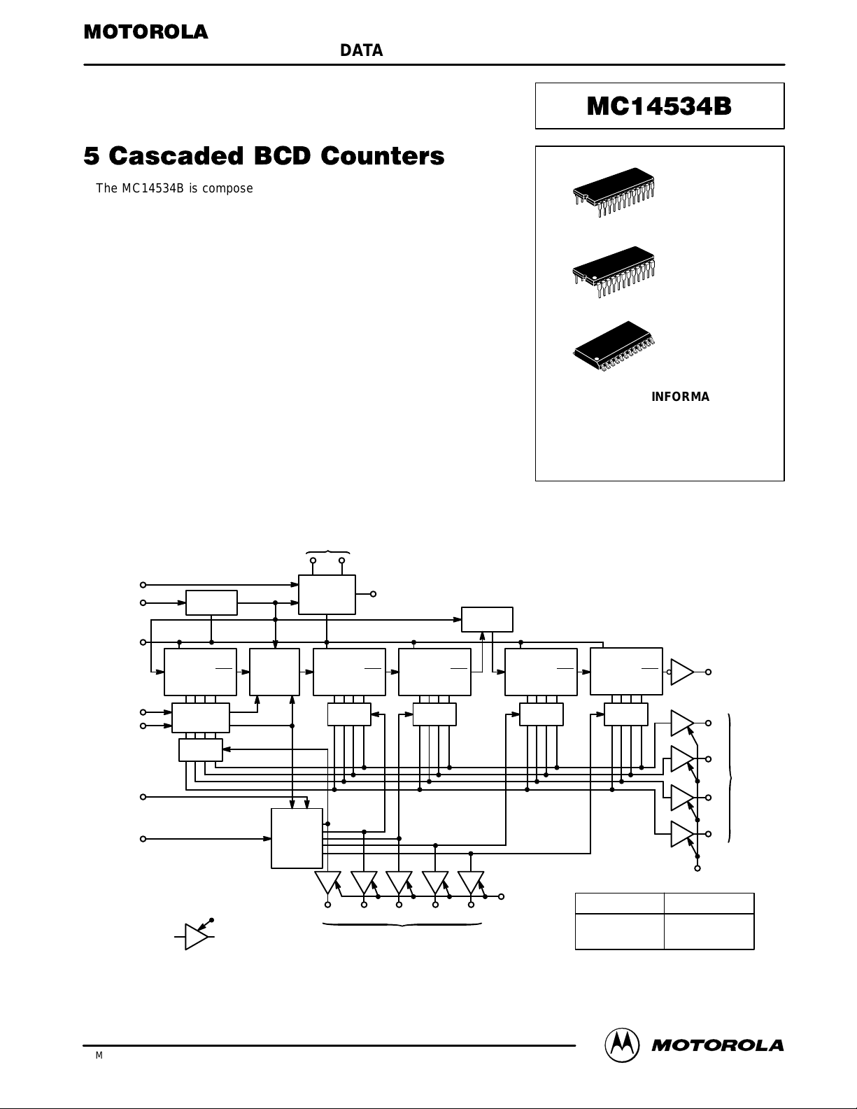
The MC14534B is composed of five BCD ripple counters that have their
respective outputs multiplexed using an internal scanner. Outputs of each
counter are selected by the scanner and appear on four (BCD) p ins.
Selection is indicated by a logic high on the appropriate digit select pin. Both
BCD and digit select outputs have three–state controls providing an
“open–circuit” when these controls are high and allowing multiplexing.
Cascading may be accomplished by using the carry–out pin. The counters
and scanner can be independently reset by applying a high to the counter
master reset (MR) and the scanner r eset (SR). The MC14534B was
specifically designed for application in real time or event counters where
continual updating and multiplexed displays are used.
• Four Operating Modes (See truth table)
• Input Error Detection Circuit
• Clock Conditioning Circuits for Slow Transition Inputs
• Counter Sequences on Positive Transition of Clock A
• Supply Voltage Range = 3.0 Vdc to 18 Vdc
• Capable of Driving Two Low–power TTL Loads or One Low–power
Schottky TTL Load Over the Rated Temperature Range
BLOCK DIAGRAM
PULSE ERROR
DETECTOR
PULSE
SHAPER
TEST
CONTROL
OUTPUT
CONTROL
MUX
MUX MUX MUX MUX
UNITS
CARRY
CONTROL
TENS HUNDREDS THOUSANDS TEN
THOUSANDS
C
÷
10 C ÷ 10 C ÷ 10 C ÷ 10 C ÷ 10
Q0 Q3 Q0 Q3 Q0 Q3 Q0 Q3 Q0 Q3
C
n+4
C
n+4
C
n+4
C
n+4
C
n+4
22
7 8 14 16 11
1
23
4
2
5
6
9
10
CLOCK B
CLOCK A
MASTER
RESET
MODE A
MODE B
SCANNER
RESET
SCANNER
CLOCK
ERROR OUT
3
R
SCANNER
13
17
18
19
20
Q3
Q2
Q1
Q0
21
3–STATE BCD
CONTROL
CARRY OUT
3–STATE DIGIT
CONTROL
15
DS1 DS2 DS3 DS4 DS5
DIGIT SELECT
3–STATE
OUTPUT BUFFER
NOTE:
BCD
OUT
VDD = PIN 24
VSS = PIN 12
TO CAPACITORS
3–State Control Out
Q or DS
High Impedance
0
1
=
SEMICONDUCTOR TECHNICAL DATA
Motorola, Inc. 1995
REV 3
1/94
L SUFFIX
CERAMIC
CASE 623
ORDERING INFORMATION
MC14XXXBCP Plastic
MC14XXXBCL Ceramic
MC14XXXBDW SOIC
TA = – 55° to 125°C for all packages.
P SUFFIX
PLASTIC
CASE 709
DW SUFFIX
SOIC
CASE 751E
Page 2
MOTOROLA CMOS LOGIC DATAMC14534B
2
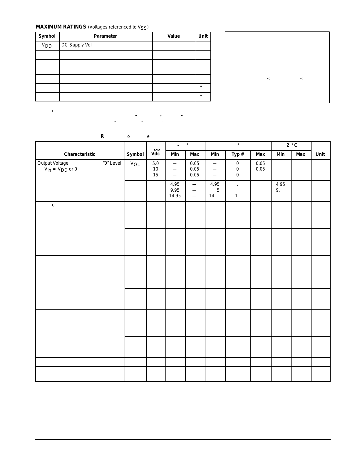
MAXIMUM RATINGS (Voltages referenced to V
SS
)
Symbol
Parameter Value Unit
V
DD
DC Supply Voltage – 0.5 to + 18.0 V
Vin, V
out
Input or Output Voltage (DC or Transient) – 0.5 to VDD + 0.5 V
Iin, I
out
Input or Output Current (DC or Transient),
per Pin
± 10 mA
P
D
Power Dissipation, per Package† 500 mW
T
stg
Storage Temperature – 65 to + 150
_
C
T
L
Lead Temperature (8–Second Soldering) 260
_
C
*Maximum Ratings are those values beyond which damage to the device may occur.
†Temperature Derating:
Plastic “P and D/DW” Packages: – 7.0 mW/_C From 65_C To 125_C
Ceramic “L” Packages: – 12 mW/_C From 100_C To 125_C
ELECTRICAL CHARACTERISTICS (Voltages Referenced to V
SS
)
V
– 55_C 25_C 125_C
Characteristic
Symbol
V
DD
Vdc
Min Max Min Typ # Max Min Max
Unit
V
OL
5.0
10
15
—
—
—
0.05
0.05
0.05
—
—
—
0
0
0
0.05
0.05
0.05
—
—
—
0.05
0.05
0.05
Vdc
V
OH
5.0
10
15
4.95
9.95
14.95
—
—
—
4.95
9.95
14.95
5.0
10
15
—
—
—
4.95
9.95
14.95
—
—
—
Vdc
V
IL
5.0
10
15
—
—
—
1.0
2.0
3.0
—
—
—
1.5
3.0
4.5
1.0
2.0
3.0
—
—
—
1.0
2.0
3.0
Vdc
V
IH
5.0
10
15
4.0
8.0
12
—
—
—
4.0
8.0
12
3.5
7.0
11
—
—
—
4.0
8.0
12
—
—
—
Vdc
I
OH
5.0
5.0
10
15
– 3.0
– 0.64
– 1.6
– 4.2
—
—
—
—
– 2.4
– 0.51
– 1.3
– 3.4
– 4.2
– 0.88
– 2.25
– 8.8
—
—
—
—
– 1.7
– 0.36
– 0.9
– 2.4
—
—
—
—
mAdc
I
OL
5.0
10
15
0.64
1.6
4.2
—
—
—
0.51
1.3
3.4
0.88
2.25
8.8
—
—
—
0.36
0.9
2.4
—
—
—
mAdc
I
OH
5.0
10
15
– 0.31
– 0.31
– 0.9
—
—
– 0.25
– 0.25
– 0.75
– 0.8
– 0.4
– 1.6
—
—
– 0.17
– 0.17
– 0.51
—
—
mAdc
I
OL
5.0
10
15
0.024
0.06
1.3
—
—
—
0.02
0.05
0.25
0.03
0.09
1.63
—
—
—
0.014
0.035
0.175
—
—
—
mAdc
Input Current I
in
15 — ± 0.1 — ± 0.00001 ± 0.1 — ± 1.0 µAdc
Input Capacitance
(Vin = 0)
C
in
— — — — 5.0 7.5 — — pF
#Data labelled “Typ” is not to be used for design purposes but is intended as an indication of the IC’s potential performance. (continued)
This device contains protection circuitry to
guard against damage due to high static
voltages or electric fields. However, precautions must be taken to avoid applications of
any voltage higher than maximum rated voltages to this high–impedance circuit. For proper
operation, Vin and V
out
should be constrained
to the range VSS v (Vin or V
out
) v VDD.
Unused inputs must always be tied to an
appropriate logic voltage level (e.g., either V
SS
or VDD). Unused outputs must be left open.
Output Voltage “0” Level
Vin = VDD or 0
Vin = 0 or V
Input Voltage “0” Level
(VO = 4.5 or 0.5 Vdc)
(VO = 9.0 or 1.0 Vdc)
(VO = 13.5 or 1.5 Vdc)
(VO = 0.5 or 4.5 Vdc)
(VO = 1.0 or 9.0 Vdc)
(VO = 1.5 or 13.5 Vdc)
Output Drive Current
(VOH = 2.5 Vdc) Source
(VOH = 4.6 Vdc)
(VOH = 9.5 Vdc)
(VOH = 13.5 Vdc)
(VOL = 0.4 Vdc) Sink
(VOL = 0.5 Vdc)
(VOL = 1.5 Vdc)
Output Drive Current — Pins 1 and 22
(VOH = 2.5 Vdc)
(VOH = 9.5 Vdc) Source
(VOH = 13.5 Vdc)
(VOL = 0.4 Vdc) Sink
(VOL = 0.5 Vdc)
(VOL = 1.5 Vdc)
DD
“1” Level
“1” Level
Page 3
MOTOROLA CMOS LOGIC DATA
3
MC14534B
ELECTRICAL CHARACTERISTICS (Voltages Referenced to V
SS
) (continued)
V
– 55_C 25_C 125_C
Characteristic
Symbol
V
DD
Vdc
Min Max Min Typ # Max Min Max
Unit
Quiescent Current
(Per Package)
I
DD
5.0
10
15
—
—
—
5.0
10
20
—
—
—
0.010
0.020
0.030
5.0
10
20
—
—
—
150
300
600
µAdc
Total Supply Current**†
(Dynamic plus Quiescent,
Per Package)
(CL = 50 pF on all outputs, all
buffers switching)
I
T
5.0
10
15
IT = (0.5 µA/kHz) f + I
DD Scan Oscillator
IT = (1.0 µA/kHz) f + I
DD Frequency = 1.0 kHz
IT = (1.5 µA/kHz) f + I
DD
µAdc
Three–State Leakage Current I
TL
15 — ± 0.1 — ± 0.0001 ± 0.1 — ± 3.0 µAdc
#Data labelled “Typ” is not to be used for design purposes but is intended as an indication of the IC’s potential performance.
**The formulas given are for the typical characteristics only at 25_C.
†To calculate total supply current at loads other than 50 pF:
IT(CL) = IT(50 pF) + (CL – 50) Vfk
where: IT is in µA (per package), CL in pF, V = (VDD – VSS) in volts, f in kHz is input frequency, and k = 0.001.
Page 4

MOTOROLA CMOS LOGIC DATAMC14534B
4
SWITCHING CHARACTERISTICS* (C
L
= 50 pF, TA = 25_C, see Figure 1)
Characteristic Symbol
V
DD
Vdc
Min Typ # Max Unit
Output Rise and Fall Time t
TLH
,
t
THL
5.0
10
15
—
—
—
100
50
40
200
100
80
ns
t
PLH
,
t
PHL
5.0
10
15
—
—
—
4.0
1.5
1.0
8.0
3.0
2.25
µs
t
PLH
5.0
10
15
—
—
—
3.3
1.1
0.8
6.6
2.2
1.7
µs
t
PHL
5.0
10
15
—
—
—
1.8
0.6
0.5
3.6
1.2
0.9
µs
t
PHL
5.0
10
15
—
—
—
0.6
0.2
0.12
1.5
.5
0.38
µs
t
PLH
,
t
PHL
5.0
10
15
—
—
—
1.8
0.6
0.5
3.6
1.2
0.9
µs
t
PLH
,
t
PLH
5.0
10
15
—
—
—
1.5
0.5
0.4
3.0
1.0
0.75
µs
t
PHZ
5.0
10
15
—
—
—
75
45
40
150
90
80
ns
t
PZH
5.0
10
15
—
—
—
120
55
40
240
110
80
ns
t
PLZ
5.0
10
15
—
—
—
120
55
45
240
110
90
ns
t
PZL
5.0
10
15
—
—
—
160
70
45
320
140
90
ns
Clock Pulse Frequency f
cl
5.0
10
15
—
—
—
1.0
3.0
5.0
0.5
1.0
1.2
MHz
Clock or Scanner Clock Pulse Width t
WH
5.0
10
15
1000
500
375
500
190
125
—
—
—
ns
Scanner Reset Pulse Width t
w
5.0
10
15
320
130
80
160
65
40
—
—
—
ns
Scanner Reset Removal Time t
rem
5.0
10
15
900
150
100
270
80
50
—
—
—
ns
Master Reset Pulse Width t
WH(R)
5.0
10
15
2000
600
450
900
300
250
—
—
—
ns
Master Reset Removal Time t
rem
5.0
10
15
1060
350
250
550
205
140
—
—
—
ns
*The formulas given are for the typical characteristics only at 25_C.
#Data labelled “Typ” is not to be used for design purposes but is intended as an indication of the IC’s potential performance.
Propagation Delay Time,
Clock to Q
t
, t
PLH
t
PLH
t
PLH
Clock to Carry Out
t
PLH
t
PLH
t
PLH
Master Reset to Q
t
PHL
t
PHL
t
PHL
Master Reset to Error Out
t
PHL
t
PHL
t
PHL
Scanner Clock to Q
t
PLH, tPHL
t
PLH
t
PLH
Scanner Clock to Digit Select
t
PHL
t
PHL
t
PHL
Propagation Delay Time
3–State Control to Q
= (1.8 ns/pF) CL + 4.0 µs
PHL
, t
= (0.8 ns/pF) CL + 1.5 µs
PHL
, t
= (0.6 ns/pF) CL + 1.0 µs
PHL
= (1.8 ns/pF) CL + 3.3 µs
= (0.8 ns/pF) CL + 1.1 µs
= (0.6 ns/pF) CL + 0.8 µs
= (1.8 ns/pF) CL + 1.8 µs
= (0.8 ns/pF) CL + 0.6 µs
= (0.6 ns/pF) CL + 0.5 µs
= (1.8 ns/pF) CL + 0.57 µs
= (0.8 ns/pF) CL + 0.19 µs
= (0.6 ns/pF) CL + 0.11 µs
= (1.8 ns/pF) CL + 1.8 µs
, t
= (0.8 ns/pF) CL + 0.6 µs
PHL
, t
= (0.6 ns/pF) CL + 0.5 µs
PHL
, t
= (1.8 ns/pF) CL + 1.5 µs
PLH
, t
= (0.8 ns/pF) CL + 0.5 µs
PLH
, t
= (0.6 ns/pF) CL + 0.4 µs
PLH
Page 5

MOTOROLA CMOS LOGIC DATA
5
MC14534B
COUNTER TIMING DIAGRAM
10
6
10
5
10
4
10
3
10
2
10987654321
CLOCK A
UNITS Q0
UNITS Q1
UNITS Q2
UNITS Q3
UNITS C
n+4
TENS Q0
TENS Q3
TENS C
n+4
HUNDREDS Q0
HUNDREDS Q3
HUNDREDS C
n+4
THOUSANDS Q0
THOUSANDS Q3
THOUSANDS C
n+4
TEN THOUSANDS Q0
TEN THOUSANDS Q3
CARRY OUT
MASTER RESET
MODE CONTROL TRUTH TABLE
Mode A Mode B First Stage Output Carry to Second Stage Application
0 0 Normal Count and Display At 9 to 0 transition of first stage 5–digit Counter
0 1 Inhibited Input Clock Test Mode: Clock directly into stages 1, 2, and 4.
1 1 Inhibited At 4 to 5 transition of first stage 4–digit counter with ÷ 10 and roundoff at front end.
1 0 Counts 3, 4, 5, 6, 7 = 5
Counts 8, 9, 0, 1, 2 = 0
At 7 to 8 transition of first stage 4–digit counter with 1/2 pence capability.
Page 6

MOTOROLA CMOS LOGIC DATAMC14534B
6
SCANNER TIMING DIAGRAM
NOTE: If Mode B = 1, the first decade is inhibited and S1 will not go high, and the cycle will be
shortened to four stages.
DS5 is selected automatically when Scanner Reset goes high.
TEN
THOUSANDS
THOUSANDS
HUNDREDS
TENS
UNITS
SCANNER
CLOCK
SCANNER
RESET
DS1
DS2
DS3
DS4
DS5
ERROR DETECTION TIMING DIAGRAM
NOTE: Error detector looks for inverted pulse on Clock B. Whenever a positive edge at
Clock A is not accompanied by a negative pulse at Clock B (or vice–versa) within
a time period of the one–shots an error is counted. Three errors result in Error Out
to go to a “1”. If error detection is not needed, tie Clock B high or low and leave
Pins 1 and 22 unconnected.
CLOCK A
CLOCK B
RESET
ERROR
OUT
GOOD PULSE
ERROR1ERROR
2
ERROR3ERROR
4
GOOD PULSE
CLOCK SKEW RANGE
NOTES:
1. The skew is the time difference between the
low–to–high transition of CA to the high–to–
low transition of CB or vice–versa. Capacitors
C1 = C22 tied from pins 1 and 22 to VSS.
2. This graph is accurate for C1 = C22 ≥ 100 pF.
3. When the error detection circuitry in not used,
pins 1 and 22 are left open.
1000
500
300
100
50
30
10
5.0
3.0
1.0
3.0 5.0 7.0 9.0 11 13 15 17
VDD (Vdc)
SKEW IN THIS RANGE
RESULTS IN COUNTED
ERROR.
MAX
SKEW IN THIS RANGE
RESULTS IN NO ERROR
COUNTED.
TYP
MIN
SKEW IN THIS RANGE
MAY OR MAY NOT
RESULT IN COUNTED
ERROR.
ALLOWABLE CLOCK SKEW (ns/pF)
Page 7

MOTOROLA CMOS LOGIC DATA
7
MC14534B
APPLICATIONS INFORMATION
Figure 1. Cascade Operation
*Carry Out is high for a single clock period when all five BCD stages go to zero.
(Carry Out also goes high when MR is applied.)
V
DD
CLOCK
CLOCK A CLOCK A
En
C
Q4 C
out
*
1/2
MC14518B
MC14534B MC14534B
Figure 2. Forcing a BCD Stage to the Q Outputs
When the Q outputs of a given stage are required, this configuration will
lock up the selected stage within four clock cycles. The select line feedback
may be hardwired or switched.
CLOCK
BCD FOR
SELECTED
STAGE
Q0
CLOCK A
Q1
Q2
Q3
SC
DS5DS4DS3DS2DS1
MC14534B
MODE B
CLOCK A
E
out
MR
C
ext
DS2
DS1
MODE A Q0
3–ST BCD
C
ext
CLOCK B
V
DD
3–ST DIG
DS4
Q3
5
4
3
2
1
10
9
8
7
6
14
15
16
17
18
19
20
13
11
12
21
22
23
24
C
out
DS3
Q2
Q1
DS5
V
SS
SC
SR
PIN ASSIGNMENT
Page 8

MOTOROLA CMOS LOGIC DATAMC14534B
8
OUTLINE DIMENSIONS
P SUFFIX
PLASTIC DIP PACKAGE
CASE 709–02
ISSUE C
L SUFFIX
CERAMIC DIP PACKAGE
CASE 623–05
ISSUE M
NOTES:
1. POSITIONAL TOLERANCE OF LEADS (D),
SHALL BE WITHIN 0.25 (0.010) AT MAXIMUM
MATERIAL CONDITION, IN RELATION TO
SEATING PLANE AND EACH OTHER.
2. DIMENSION L TO CENTER OF LEADS WHEN
FORMED PARALLEL.
3. DIMENSION B DOES NOT INCLUDE MOLD
FLASH.
DIM MIN MAX MIN MAX
INCHESMILLIMETERS
A 31.37 32.13 1.235 1.265
B 13.72 14.22 0.540 0.560
C 3.94 5.08 0.155 0.200
D 0.36 0.56 0.014 0.022
F 1.02 1.52 0.040 0.060
G 2.54 BSC 0.100 BSC
H 1.65 2.03 0.065 0.080
J 0.20 0.38 0.008 0.015
K 2.92 3.43 0.115 0.135
L 15.24 BSC 0.600 BSC
M 0 15 0 15
N 0.51 1.02 0.020 0.040
_ _ _ _
1 12
1324
B
H
A
F
D
G
K
SEATING
PLANE
N
C
M
J
L
NOTES:
1. DIMENSION L TO CENTER OF LEADS WHEN
FORMED PARALLEL.
2. LEADS WITHIN 0.13 (0.005) RADIUS OF TRUE
POSITION AT SEATING PLANE AT MAXIMUM
MATERIAL CONDITION (WHEN FORMED
PARALLEL).
1 12
24 13
B
A
SEATING
PLANE
F
D
G
K
N
C
M
J
L
DIM MIN MAX MIN MAX
INCHESMILLIMETERS
A 31.24 32.77 1.230 1.290
B 12.70 15.49 0.500 0.610
C 4.06 5.59 0.160 0.220
D 0.41 0.51 0.016 0.020
F 1.27 1.52 0.050 0.060
G 2.54 BSC 0.100 BSC
J 0.20 0.30 0.008 0.012
K 3.18 4.06 0.125 0.160
L 15.24 BSC 0.600 BSC
M 0 15 0 15
N 0.51 1.27 0.020 0.050
_ _ _ _
Page 9

MOTOROLA CMOS LOGIC DATA
9
MC14534B
OUTLINE DIMENSIONS
DW SUFFIX
PLASTIC SOIC PACKAGE
CASE 751E–04
ISSUE E
NOTES:
1. DIMENSIONING AND TOLERANCING PER ANSI
Y14.5M, 1982.
2. CONTROLLING DIMENSION: MILLIMETER.
3. DIMENSIONS A AND B DO NOT INCLUDE
MOLD PROTRUSION.
4. MAXIMUM MOLD PROTRUSION 0.15 (0.006)
PER SIDE.
5. DIMENSION D DOES NOT INCLUDE DAMBAR
PROTRUSION. ALLOWABLE DAMBAR
PROTRUSION SHALL BE 0.13 (0.005) TOTAL IN
EXCESS OF D DIMENSION AT MAXIMUM
MATERIAL CONDITION.
–A–
–B– P12X
D24X
12
1324
1
M
0.010 (0.25) B
M
S
A
M
0.010 (0.25) B
S
T
–T–
G
22X
SEATING
PLANE
K
C
R
X 45
_
M
F
J
DIM MIN MAX MIN MAX
INCHESMILLIMETERS
A 15.25 15.54 0.601 0.612
B 7.40 7.60 0.292 0.299
C 2.35 2.65 0.093 0.104
D 0.35 0.49 0.014 0.019
F 0.41 0.90 0.016 0.035
G 1.27 BSC 0.050 BSC
J 0.23 0.32 0.009 0.013
K 0.13 0.29 0.005 0.011
M 0 8 0 8
P 10.05 10.55 0.395 0.415
R 0.25 0.75 0.010 0.029
____
How to reach us:
USA/EUROPE/Locations Not Listed: Motorola Literature Distribution; JAPAN: Nippon Motorola Ltd.; Tatsumi–SPD–JLDC, 6F Seibu–Butsuryu–Center,
P.O. Box 20912; Phoenix, Arizona 85036. 1–800–441–2447 or 602–303–5454 3–14–2 Tatsumi Koto–Ku, Tokyo 135, Japan. 03–81–3521–8315
MFAX: RMFAX0@email.sps.mot.com – TOUCHTONE 602–244–6609 ASIA/PACIFIC: Motorola Semiconductors H.K. Ltd.; 8B Tai Ping Industrial Park,
INTERNET: http://Design–NET.com 51 Ting Kok Road, Tai Po, N.T., Hong Kong. 852–26629298
Motorola reserves the right to make changes without further notice to any products herein. Motorola makes no warranty , representation or guarantee regarding
the suitability of its products for any particular purpose, nor does Motorola assume any liability arising out of the application or use of any product or circuit,
and specifically disclaims any and all liability, including without limitation consequential or incidental damages. “Typical” parameters which may be provided
in Motorola data sheets and/or specifications can and do vary in different applications and actual performance may vary over time. All operating parameters,
including “Typicals” must be validated for each customer application by customer’s technical experts. Motorola does not convey any license under its patent
rights nor the rights of others. Motorola products are not designed, intended, or authorized for use as components in systems intended for surgical implant
into the body, or other applications intended to support or sustain life, or for any other application in which the failure of the Motorola product could create a
situation where personal injury or death may occur. Should Buyer purchase or use Motorola products for any such unintended or unauthorized application,
Buyer shall indemnify and hold Motorola and its officers, employees, subsidiaries, affiliates, and distributors harmless against all claims, costs, damages, and
expenses, and reasonable attorney fees arising out of, directly or indirectly, any claim of personal injury or death associated with such unintended or
unauthorized use, even if such claim alleges that Motorola was negligent regarding the design or manufacture of the part. Motorola and are registered
trademarks of Motorola, Inc. Motorola, Inc. is an Equal Opportunity/Affirmative Action Employer .
MC14534B/D
*MC14534B/D*
◊
 Loading...