

Page 1
MOTOROLA CMOS LOGIC DATA
1
MC14530B
The MC14530B dual five–input majority logic gate is constructed with
P–channel a nd N –channel e nhancement mode d evices i n a single
monolithic structure. Combinational and sequential logic expressions are
easily implemented with the majority logic gate, often resulting in fewer
components than obtainable with the more basic gates. This device can also
provide numerous logic functions by using the W and some of the logic (A
thru E) inputs as control inputs.
• Diode Protection on All Inputs
• Supply Voltage Range = 3.0 Vdc to 18 Vdc
• Capable of Driving Two Low–power TTL Loads or One Low–power
Schottky TTL Load Over the Rated Temperature Range
MAXIMUM RATINGS* (Voltages Referenced to V
SS
)
Symbol
Parameter
Value
Unit
V
DD
DC Supply Voltage
– 0.5 to + 18.0
V
Vin, V
out
Input or Output Voltage (DC or Transient)
– 0.5 to VDD + 0.5
V
Iin, I
out
Input or Output Current (DC or Transient),
per Pin
± 10
mA
P
D
Power Dissipation, per Package†
500
mW
T
stg
Storage Temperature
– 65 to + 150
_
C
T
L
Lead Temperature (8–Second Soldering)
260
_
C
*Maximum Ratings are those values beyond which damage to the device may occur.
†Temperature Derating:
Plastic “P and D/DW” Packages: – 7.0 mW/_C From 65_C To 125_C
Ceramic “L” Packages: – 12 mW/_C From 100_C To 125_C
LOGIC TABLE
INPUTS A B C D E W Z
0 1
more inputs are logical “0”.
1 0
0 0
more inputs are logical “1”.
1 1
This device contains protection circuitry to guard against damage
due to high static voltages or electric fields. However, precautions must
be taken to avoid applications of any voltage higher than maximum rated
voltages to this high-impedance circuit. For proper operation, Vin and
V
out
should be constrained to the range VSS ≤ (Vin or V
out
) ≤ VDD.
Unused inputs must always be tied to an appropriate logic voltage
level (e.g., either VSS or VDD). Unused outputs must be left open.
SEMICONDUCTOR TECHNICAL DATA
Motorola, Inc. 1995
REV 3
1/94
L SUFFIX
CERAMIC
CASE 620
ORDERING INFORMATION
MC14XXXBCP Plastic
MC14XXXBCL Ceramic
MC14XXXBD SOIC
TA = – 55° to 125°C for all packages.
P SUFFIX
PLASTIC
CASE 648
D SUFFIX
SOIC
CASE 751B
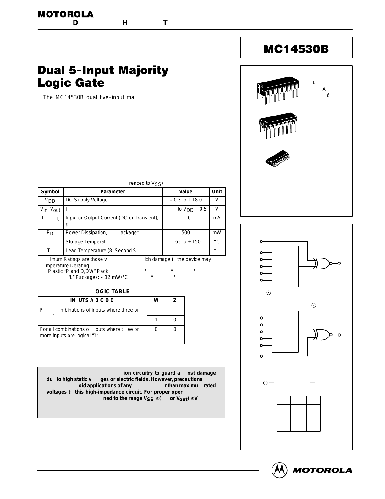
BLOCK DIAGRAM
TRUTH TABLE
M5W Z
0 0 1
0 1 0
1 0 0
1 1 1
VDD = PIN 16
VSS = PIN 8
A
W
1
B
C
D
E
2
3
4
5
6
Z
7
M
5
A
B
C
D
E
M
5
13
12
11
10
9
14
W
Z
15
*Z = M5 W = (ABC+ABD+ABE+ACD+
Z = M5 W = (ACE+ADE+BCD+BCE+
Z = M5 W = (BDE+CDE) W
*M5 is a logical “1” if any three or more
inputs are logical “1”.
Exclusive NOR Exclusive OR
For all combinations of inputs where three or
For all combinations of inputs where three or
Page 2
MOTOROLA CMOS LOGIC DATAMC14530B
2
ELECTRICAL CHARACTERISTICS (Voltages Referenced to V
SS
)
V
– 55_C 25_C 125_C
Characteristic
Symbol
V
DD
Vdc
Min Max Min Typ # Max Min Max
Unit
“0” Level
Vin = VDD or 0
V
OL
5.0
10
15
—
—
—
0.05
0.05
0.05
—
—
—
0
0
0
0.05
0.05
0.05
—
—
—
0.05
0.05
0.05
Vdc
“1” Level
Vin = 0 or V
DD
V
OH
5.0
10
15
4.95
9.95
14.95
—
—
—
4.95
9.95
14.95
5.0
10
15
—
—
—
4.95
9.95
14.95
—
—
—
Vdc
“0” Level
(VO = 4.5 or 0.5 Vdc)
(VO = 9.0 or 1.0 Vdc)
(VO = 13.5 or 1.5 Vdc)
V
IL
5.0
10
15
—
—
—
1.2
2.5
3.0
—
—
—
2.25
4.50
6.75
1.25
2.5
3.0
—
—
—
1.15
2.4
2.9
Vdc
“1” Level
(VO = 0.5 or 4.5 Vdc)
(VO = 1.0 or 9.0 Vdc)
(VO = 1.5 or 13.5 Vdc)
V
IH
5.0
10
15
3.85
7.6
12.1
—
—
—
3.75
7.5
12
2.75
5.50
8.25
—
—
—
3.75
7.5
12
—
—
Vdc
I
OH
5.0
5.0
10
15
– 3.0
– 0.64
– 1.6
– 4.2
—
—
—
—
– 2.4
– 0.51
– 1.3
– 3.4
– 4.2
– 0.88
– 2.25
– 8.8
—
—
—
—
– 1.7
– 0.36
– 0.9
– 2.4
—
—
—
—
mAdc
I
OL
5.0
10
15
0.64
1.6
4.2
—
—
—
0.51
1.3
3.4
0.88
2.25
8.8
—
—
—
0.36
0.9
2.4
—
—
—
mAdc
Input Current I
in
15 — ± 0.1 — ±0.00001 ± 0.1 — ± 1.0 µAdc
Input Capacitance
(Vin = 0)
C
in
— — — — 5.0 7.5 — — pF
Quiescent Current
(Per Package)
I
DD
5.0
10
15
—
—
—
0.25
0.5
1.0
—
—
—
0.0005
0.0010
0.0015
0.25
0.5
1.0
—
—
—
7.5
15
30
µAdc
Total Supply Current**†
(Dynamic plus Quiescent,
Per Package)
(CL = 50 pF on all outputs, all
buffers switching)
I
T
5.0
10
15
IT = (0.75 µA/kHz) f + I
DD
IT = (1.50 µA/kHz) f + I
DD
IT = (2.25 µA/kHz) f + I
DD
µAdc
#Data labelled “Typ” is not to be used for design purposes but is intended as an indication of the IC’s potential performance.
**The formulas given are for the typical characteristics only at 25_C.
*To calculate total supply current at loads other than 50 pF:
IT(CL) = IT(50 pF) + (CL – 50) Vfk
where: IT is in µA (per package), CL in pF, V = (VDD – VSS) in volts, f in kHz is input frequency, and k = 0.002.
PIN ASSIGNMENT
13
14
15
16
9
10
11
125
4
3
2
1
8
7
6
D
B
E
B
W
B
Z
B
V
DD
A
B
B
B
C
B
D
A
C
A
B
A
A
A
V
SS
Z
A
W
A
E
A
Output Voltage
Input Voltage
Output Drive Current
(VOH = 2.5 Vdc) Source
(VOH = 4.6 Vdc)
(VOH = 9.5 Vdc)
(VOH = 13.5 Vdc)
(VOL = 0.4 Vdc) Sink
(VOL = 0.5 Vdc)
(VOL = 1.5 Vdc)
Page 3
MOTOROLA CMOS LOGIC DATA
3
MC14530B
SWITCHING CHARACTERISTICS* (C
L
= 50 pF, TA = 25_C)
Characteristic
Symbol V
DD
Min Typ # Max Unit
Output Rise and Fall Time
t
TLH
, t
THL
= (1.5 ns/pF) CL + 25 ns
t
TLH
, t
THL
= (0.75 ns/pF) CL + 12.5 ns
t
TLH
, t
THL
= (0.55 ns/pF) CL + 9.5 ns
t
TLH
,
t
THL
5.0
10
15
—
—
—
100
50
40
200
100
80
ns
t
PLH
5.0
10
15
—
—
—
375
160
110
960
400
300
ns
t
PHL
5.0
10
15
—
—
—
430
195
120
1200
540
410
ns
t
PLH
5.0
10
15
—
—
—
255
120
86
640
300
210
ns
t
PHL
5.0
10
15
—
—
—
280
125
100
750
330
250
ns
A, B, C, D, E = Gnd; W = Pulse Generator
t
PHL
, t
PLH
= (1.7 ns/pF) CL + 145 ns
t
PHL
, t
PLH
= (0.66 ns/pF) CL + 72 ns
t
PHL
, t
PLH
= (0.5 ns/pF) CL + 50 ns
t
PLH
,
t
PHL
5.0
10
15
—
—
—
230
105
75
575
265
190
ns
*The formulas given are for the typical characteristics only at 25_C.
#Data labelled “Typ” is not to be used for design purposes but is intended as an indication of the IC’s potential performance.
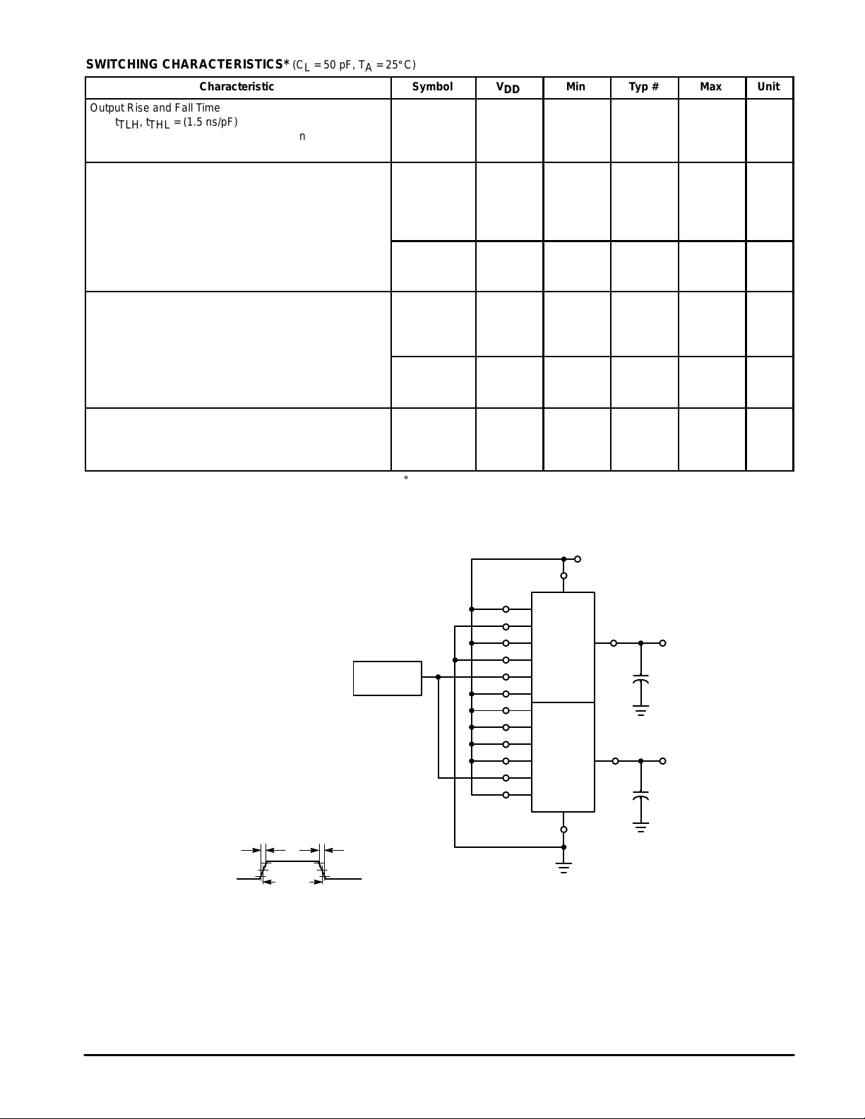
Figure 1. Power Dissipation Test
Circuit and Waveform
A
B
C
D
E
W
A
B
C
D
E
W
PULSE
GENERATOR
V
DD
V
SS
C
L
C
L
Z
Z
8
16
V
DD
V
SS
20 ns 20 ns
V
in
50%
DUTY
CYCLE
Propagation Delay Time
A, C, W = VDD; B, E = Gnd; D = Pulse Generator
t
PLH
t
PLH
t
PLH
t
PHL
t
PHL
t
PHL
A, B, C, D, E = Pulse Generator; W = V
t
PLH
t
PLH
t
PLH
t
PHL
t
PHL
t
PHL
= (1.7 ns/pF) CL + 290 ns
= (0.66 ns/pF) CL + 127 ns
= (0.5 ns/pF) CL + 85 ns
= (1.7 ns/pF) CL + 345 ns
= (0.66 ns/pF) CL + 162 ns
= (0.5 ns/pF) CL + 95 ns
= (1.7 ns/pF) CL + 170 ns
= (0.66 ns/pF) CL + 87 ns
= (0.5 ns/pF) CL + 60 ns
= (1.7 ns/pF) CL + 195 ns
= (0.66 ns/pF) CL + 92 ns
= (0.5 ns/pF) CL + 75 ns
DD
Page 4

MOTOROLA CMOS LOGIC DATAMC14530B
4
SEQUENTIAL LOGIC APPLICATIONS
COINCIDENT FLIP–FLOP
ASTABLE MULTIVIBRATOR
COINCIDENT FLIP–FLOP
x y Q
n+1
0 0 0
0 1 Q
0 0 Q
1 1 1
A flip–flop that will change only when both inputs agree.
x y Q
n+1
0 0 1
0 1 2τ
1 0 2τ
1 1 1
A flip–flop with three output conditions, where the third state is
in oscillation between “1” and “0”. The period of oscillation is
twice the delay of the gate and the feedback element.
t
x
y z Q
n+1
0 0 0 0
0 0 1 Q
n
0 1 0 Q
n
0 1 1 Q
n
1 0 0 Q
n
1 0 1 Q
n
1 1 0 Qn
1 1 1 1
The flip–flop changes state only when all “1’s” or all “0’s” are
entered. This configuration may be extended by cascading M
5
gates to cover n–inputs where all inputs must be “1’s” or “0’s”
before the output will change. As an example, this configuration is useful for controlling an n–stage up/down counter that is
to cycle from a minimum to maximum count and back again
without flipping over (from all “1’s” to all “0’s”.)
Z
0
W
Z
Z
A
B
C
D
E
1
1
x
y
t
0
W
A
B
C
D
E
0
1
x
y
x
W
A
B
C
D
E
1
y
z
Page 5

MOTOROLA CMOS LOGIC DATA
5
MC14530B
BASIC COMBINATIONAL FUNCTIONS 5–INPUT MAJORITY LOGIC GATE APPLICATIONS
DOUBLING THE WEIGHT OF INPUT VARIABLE A
BY TYING IT TO ANY TWO INPUTS
CORRELATION OF MULTIPLE SAMPLES
WITH A TEST BIT
The gate will have a “1” output if
the test bit To matches or correlates with 3, 4 or 5 of the sample
bits S0–S4.
1. Majority Logic Gate Array
yielding the symmetric function
of 1 thru 7 variables true, out
of 7 input variables (X1... X7)
(e.g., if any two–input variables
are true (logical “1”), Z1 and
Z2 are true (logical “1”)
Each package labeled M5 is a single majority logic gate
using five inputs, A thru E, and one output Z.
A
W
0
B
C
D
E
M
5
Z
A
W
1
B
C
D
E
M
5
Z
A
W
0
B
C
M
3
Z
1
0
A
W
1
B
C
M
3
Z
1
0
A
W
1
B
C
OR
3
Z
1
1
A
W
0
B
C
NOR
3
Z
1
1
A
W
1
B
C
AND
3
Z
0
0
A
W
0
B
C
NAND
3
Z
0
0
5–INPUT MAJORITY GATES
3–INPUT MAJORITY GATES
3–INPUT OR GATE
3–INPUT AND GATE 3–INPUT NAND GATE
3–INPUT NOR GATE
A
B
C
D
E
M
5
A
B
C
D
E
M
5
A
B
C
D
E
M
5
A
B
C
D
E
M
5
A
B
C
D
E
M
5
A
B
C
D
E
M
5
A
B
C
D
E
M
5
M
5
M
5
M
5
M
5
M
5
M
5
M
5
M
5
Z1
Z2
Z3
Z4
Z5
Z6
Z7
0
0
0
0
0
0
0
0
0
1
1
1
1
1
1
1
1
1
X1 X4 X6 X7X5X3
X2
A
A
B
C
D
Z
Z
Z
Z
W
W
A
B
C
D
E
To
W
W
W
S0
S1
S2
S3
S4
A
B
C
D
E
To
S0
S1
S2
S3
A
B
C
D
E
To
To
S0
S1
S2
CORRELATION OF 100%
CORRELATION OF 75%, 100%
CORRELATION OF 60%, 80%, 100%
(AB + AC + AD + BCD) W
To
To
Page 6

MOTOROLA CMOS LOGIC DATAMC14530B
6
OUTLINE DIMENSIONS
P SUFFIX
PLASTIC DIP PACKAGE
CASE 648–08
ISSUE R
NOTES:
1. DIMENSIONING AND TOLERANCING PER ANSI
Y14.5M, 1982.
2. CONTROLLING DIMENSION: INCH.
3. DIMENSION L TO CENTER OF LEADS WHEN
FORMED PARALLEL.
4. DIMENSION B DOES NOT INCLUDE MOLD FLASH.
5. ROUNDED CORNERS OPTIONAL.
–A–
B
F
C
S
H
G
D
J
L
M
16 PL
SEATING
1 8
916
K
PLANE
–T–
M
A
M
0.25 (0.010) T
DIM MIN MAX MIN MAX
MILLIMETERSINCHES
A 0.740 0.770 18.80 19.55
B 0.250 0.270 6.35 6.85
C 0.145 0.175 3.69 4.44
D 0.015 0.021 0.39 0.53
F 0.040 0.70 1.02 1.77
G 0.100 BSC 2.54 BSC
H 0.050 BSC 1.27 BSC
J 0.008 0.015 0.21 0.38
K 0.110 0.130 2.80 3.30
L 0.295 0.305 7.50 7.74
M 0 10 0 10
S 0.020 0.040 0.51 1.01
____
L SUFFIX
CERAMIC DIP PACKAGE
CASE 620–10
ISSUE V
NOTES:
1. DIMENSIONING AND TOLERANCING PER
ANSI Y14.5M, 1982.
2. CONTROLLING DIMENSION: INCH.
3. DIMENSION L TO CENTER OF LEAD WHEN
FORMED PARALLEL.
4. DIMENSION F MAY NARROW TO 0.76 (0.030)
WHERE THE LEAD ENTERS THE CERAMIC
BODY.
–A–
–B–
–T–
F
E
G
N
K
C
SEATING
PLANE
16 PLD
S
A
M
0.25 (0.010) T
16 PLJ
S
B
M
0.25 (0.010) T
M
L
DIM MIN MAX MIN MAX
MILLIMETERSINCHES
A 0.750 0.785 19.05 19.93
B 0.240 0.295 6.10 7.49
C ––– 0.200 ––– 5.08
D 0.015 0.020 0.39 0.50
E 0.050 BSC 1.27 BSC
F 0.055 0.065 1.40 1.65
G 0.100 BSC 2.54 BSC
H 0.008 0.015 0.21 0.38
K 0.125 0.170 3.18 4.31
L 0.300 BSC 7.62 BSC
M 0 15 0 15
N 0.020 0.040 0.51 1.01
_ _ _ _
16 9
1 8
Page 7

MOTOROLA CMOS LOGIC DATA
7
MC14530B
OUTLINE DIMENSIONS
D SUFFIX
PLASTIC SOIC PACKAGE
CASE 751B–05
ISSUE J
NOTES:
1. DIMENSIONING AND TOLERANCING PER ANSI
Y14.5M, 1982.
2. CONTROLLING DIMENSION: MILLIMETER.
3. DIMENSIONS A AND B DO NOT INCLUDE
MOLD PROTRUSION.
4. MAXIMUM MOLD PROTRUSION 0.15 (0.006)
PER SIDE.
5. DIMENSION D DOES NOT INCLUDE DAMBAR
PROTRUSION. ALLOWABLE DAMBAR
PROTRUSION SHALL BE 0.127 (0.005) TOTAL
IN EXCESS OF THE D DIMENSION AT
MAXIMUM MATERIAL CONDITION.
1 8
16 9
SEATING
PLANE
F
J
M
R
X 45
_
G
8 PLP
–B–
–A–
M
0.25 (0.010) B
S
–T–
D
K
C
16 PL
S
B
M
0.25 (0.010) A
S
T
DIM MIN MAX MIN MAX
INCHESMILLIMETERS
A 9.80 10.00 0.386 0.393
B 3.80 4.00 0.150 0.157
C 1.35 1.75 0.054 0.068
D 0.35 0.49 0.014 0.019
F 0.40 1.25 0.016 0.049
G 1.27 BSC 0.050 BSC
J 0.19 0.25 0.008 0.009
K 0.10 0.25 0.004 0.009
M 0 7 0 7
P 5.80 6.20 0.229 0.244
R 0.25 0.50 0.010 0.019
_ _ _ _
How to reach us:
USA/EUROPE/Locations Not Listed: Motorola Literature Distribution; JAPAN: Nippon Motorola Ltd.; Tatsumi–SPD–JLDC, 6F Seibu–Butsuryu–Center,
P.O. Box 20912; Phoenix, Arizona 85036. 1–800–441–2447 or 602–303–5454 3–14–2 Tatsumi Koto–Ku, Tokyo 135, Japan. 03–81–3521–8315
MFAX: RMFAX0@email.sps.mot.com – TOUCHTONE 602–244–6609 ASIA/PACIFIC: Motorola Semiconductors H.K. Ltd.; 8B Tai Ping Industrial Park,
INTERNET: http://Design–NET.com 51 Ting Kok Road, Tai Po, N.T., Hong Kong. 852–26629298
Motorola reserves the right to make changes without further notice to any products herein. Motorola makes no warranty , representation or guarantee regarding
the suitability of its products for any particular purpose, nor does Motorola assume any liability arising out of the application or use of any product or circuit,
and specifically disclaims any and all liability, including without limitation consequential or incidental damages. “Typical” parameters which may be provided
in Motorola data sheets and/or specifications can and do vary in different applications and actual performance may vary over time. All operating parameters,
including “Typicals” must be validated for each customer application by customer’s technical experts. Motorola does not convey any license under its patent
rights nor the rights of others. Motorola products are not designed, intended, or authorized for use as components in systems intended for surgical implant
into the body, or other applications intended to support or sustain life, or for any other application in which the failure of the Motorola product could create a
situation where personal injury or death may occur. Should Buyer purchase or use Motorola products for any such unintended or unauthorized application,
Buyer shall indemnify and hold Motorola and its officers, employees, subsidiaries, affiliates, and distributors harmless against all claims, costs, damages, and
expenses, and reasonable attorney fees arising out of, directly or indirectly, any claim of personal injury or death associated with such unintended or
unauthorized use, even if such claim alleges that Motorola was negligent regarding the design or manufacture of the part. Motorola and are registered
trademarks of Motorola, Inc. Motorola, Inc. is an Equal Opportunity/Affirmative Action Employer .
MC14530B/D
*MC14530B/D*
◊
 Loading...