

Datasheet MC14526BDW, MC14526BCP, MC14526BCL, MC14522BCL, MC14522BCP Datasheet (Motorola)
...Page 1
MOTOROLA CMOS LOGIC DATA
1
MC14522B MC14526B
The MC14522B BCD counter and the MC14526B binary counter are
constructed with MOS P–channel and N–channel enhancement mode
devices in a monolithic structure.
These devices are presettable, cascadable, synchronous down counters
with a decoded “0” state output for divide–by–N applications. In single stage
applications the “ 0” output is applied to the Preset Enable input. T he
Cascade Feedback input allows cascade divide–by–N operation with no
additional gates required. The Inhibit input allows disabling o f the pulse
counting function. Inhibit may also be used as a negative edge clock.
These complementary MOS counters can be used in frequency synthesizers, phase–locked loops, and other frequency division applications requiring
low power dissipation and/or high noise immunity.
• Supply Voltage Range = 3.0 Vdc to 18 Vdc
• Logic Edge–Clocked Design — Incremented on Positive Transition of
Clock or Negative Transition of Inhibit
• Asynchronous Preset Enable
• Capable of Driving Two Low–power TTL Loads or One Low–power
Schottky TTL Load Over the Rated Temperature Range
MAXIMUM RATINGS* (Voltages Referenced to V
SS
)
Symbol
Parameter Value Unit
V
DD
DC Supply Voltage – 0.5 to + 18.0 V
Vin, V
out
Input or Output Voltage (DC or Transient) – 0.5 to VDD + 0.5 V
Iin, I
out
Input or Output Current (DC or Transient),
per Pin
± 10 mA
P
D
Power Dissipation, per Package† 500 mW
T
stg
Storage Temperature – 65 to + 150
_
C
T
L
Lead Temperature (8–Second Soldering) 260
_
C
*Maximum Ratings are those values beyond which damage to the device may occur.
†Temperature Derating:
Plastic “P and D/DW” Packages: – 7.0 mW/_C From 65_C To 125_C
Ceramic “L” Packages: – 12 mW/_C From 100_C To 125_C
FUNCTION TABLE
Inputs Output
Clock Reset Inhibit
Preset
Enable
Cascade
Feedback
“0”
Resulting
Function
XXHHXXLHLLLHAsynchronous reset*
Asynchronous reset
X L X H X L Asynchronous preset
No change** (inactive edge)
LLL
LLLLLLNo change** (inactive edge)
No change** (inactive edge)
HLLLL
Decrement**
X = Don’t Care
NOTES:
*Output “0” is low when reset goes high only it PE and CF are low.
**Output “0” is high when reset is low, only if CF is high and count is 0000.
SEMICONDUCTOR TECHNICAL DATA
Motorola, Inc. 1995
REV 3
1/94
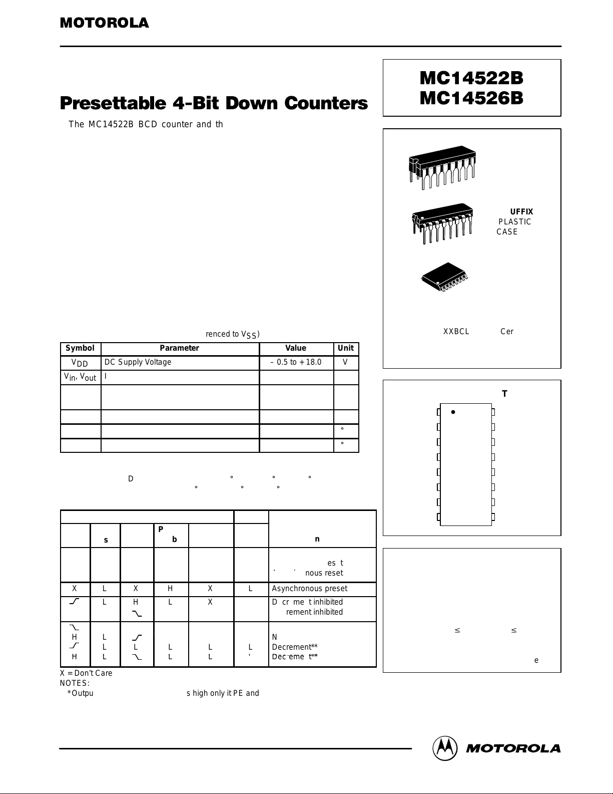
L SUFFIX
CERAMIC
CASE 620
ORDERING INFORMATION
MC14XXXBCP Plastic
MC14XXXBCL Ceramic
MC14XXXBDW SOIC
TA = – 55° to 125°C for all packages.
P SUFFIX
PLASTIC
CASE 648
DW SUFFIX
SOIC
CASE 751G
This device contains protection circuitry to
guard against damage due to high static
voltages or electric fields. However, precautions must be taken to avoid applications of
any voltage higher than maximum rated voltages to this high–impedance circuit. For proper
operation, Vin and V
out
should be constrained
to the range VSS v (Vin or V
out
) v VDD.
Unused inputs must always be tied to an
appropriate logic voltage level (e.g., either V
SS
or VDD). Unused outputs must be left open.
PIN ASSIGNMENT
13
14
15
16
9
10
11
125
4
3
2
1
8
7
6
“0”
CF
P2
Q2
V
DD
Q1
RESET
P1
INHIBIT
PE
P3
Q3
V
SS
Q0
CLOCK
P0
X
X H X X H H Asynchronous reset
L L L X L Decrement inhibited
H
H
L
L
L
X
H L
L L
L L
L
L
X
L
L
L
Asynchronous reset*
L
Decrement inhibited
L
L
Decrement**
Page 2

MOTOROLA CMOS LOGIC DATAMC14522B MC14526B
2
ELECTRICAL CHARACTERISTICS (Voltages Referenced to V
SS
)
V
DD
– 55_C 25_C 125_C
Characteristic
Symbol
DD
Vdc
Min Max Min Typ # Max Min Max
Unit
“0” Level
Vin = VDD or 0
V
OL
5.0
10
15
—
—
—
0.05
0.05
0.05
—
—
—
0
0
0
0.05
0.05
0.05
—
—
—
0.05
0.05
0.05
Vdc
“1” Level
Vin = 0 or V
DD
V
OH
5.0
10
15
4.95
9.95
14.95
—
—
—
4.95
9.95
14.95
5.0
10
15
—
—
—
4.95
9.95
14.95
—
—
—
Vdc
“0” Level
(VO = 4.5 or 0.5 Vdc)
(VO = 9.0 or 1.0 Vdc)
(VO = 13.5 or 1.5 Vdc)
V
IL
5.0
10
15
—
—
—
1.5
3.0
4.0
—
—
—
2.25
4.50
6.75
1.5
3.0
4.0
—
—
—
1.5
3.0
4.0
Vdc
“1” Level
(VO = 0.5 or 4.5 Vdc)
(VO = 1.0 or 9.0 Vdc)
(VO = 1.5 or 13.5 Vdc)
V
IH
5.0
10
15
3.5
7.0
11
—
—
—
3.5
7.0
11
2.75
5.50
8.25
—
—
—
3.5
7.0
11
—
—
—
Vdc
I
OH
5.0
5.0
10
15
– 3.0
– 0.64
– 1.6
– 4.2
—
—
—
—
– 2.4
– 0.51
– 1.3
– 3.4
– 4.2
– 0.88
– 2.25
– 8.8
—
—
—
—
– 1.7
– 0.36
– 0.9
– 2.4
—
—
—
—
mAdc
I
OL
5.0
10
15
0.64
1.6
4.2
—
—
—
0.51
1.3
3.4
0.88
2.25
8.8
—
—
—
0.36
0.9
2.4
—
—
—
mAdc
Input Current I
in
15 — ± 0.1 — ±0.00001 ± 0.1 — ± 1.0 µAdc
Input Capacitance
(Vin = 0)
C
in
— — — — 5.0 7.5 — — pF
Quiescent Current
(Per Package)
I
DD
5.0
10
15
—
—
—
5.0
10
20
—
—
—
0.005
0.010
0.015
5.0
10
20
—
—
—
150
300
600
µAdc
Total Supply Current**†
(Dynamic plus Quiescent,
Per Package)
(CL = 50 pF on all outputs, all
buffers switching)
I
T
5.0
10
15
IT = (1.7 µA/kHz) f + I
DD
IT = (3.4 µA/kHz) f + I
DD
IT = (5.1 µA/kHz) f + I
DD
µAdc
#Data labelled “Typ” is not to be used for design purposes but is intended as an indication of the IC’s potential performance.
**The formulas given are for the typical characteristics only at 25_C.
†To calculate total supply current at loads other than 50 pF:
IT(CL) = IT(50 pF) + (CL – 50) Vfk
where: IT is in µA (per package), CL in pF, V = (VDD – VSS) in volts, f in kHz is input frequency, and k = 0.001.
Output Voltage
Input Voltage
Output Drive Current
(VOH = 2.5 Vdc) Source
(VOH = 4.6 Vdc)
(VOH = 9.5 Vdc)
(VOH = 13.5 Vdc)
(VOL = 0.4 Vdc) Sink
(VOL = 0.5 Vdc)
(VOL = 1.5 Vdc)
Page 3

MOTOROLA CMOS LOGIC DATA
3
MC14522B MC14526B
SWITCHING CHARACTERISTICS* (C
L
= 50 pF, TA = 25_C)
Characteristic
Symbol V
DD
Min Typ # Max Unit
Output Rise and Fall Time
t
TLH
, t
THL
= (1.5 ns/pF) CL + 25 ns
t
TLH
, t
THL
= (0.75 ns/pF) CL + 12.5 ns
t
TLH
, t
THL
= (0.55 ns/pF) CL + 9.5 ns
t
TLH
,
t
THL
(Figures 4, 5)
5.0
10
15
—
—
—
100
50
40
200
100
80
ns
5.0
10
15
—
—
—
550
225
160
1100
450
320
5.0
10
15
—
—
—
240
130
100
480
260
200
Propagation Delay Time
Pn to Q
t
PLH
,
t
PHL
(Figures 4, 7)
5.0
10
15
—
—
—
260
120
100
520
240
200
ns
Propagation Delay Time
Reset to Q
t
PHL
(Figure 8)
5.0
10
15
—
—
—
250
110
80
500
220
160
ns
Propagation Delay Time
Preset Enable to “0”
t
PHL
,
t
PLH
(Figures 4, 9)
5.0
10
15
—
—
—
220
100
80
440
200
160
ns
Clock or Inhibit Pulse Width t
w
(Figures 5, 6)
5.0
10
15
250
100
80
125
50
40
—
—
—
ns
Clock Pulse Frequency (with PE = low) f
max
(Figures 4, 5, 6)
5.0
10
15
—
—
—
2.0
5.0
6.6
1.5
3.0
4.0
MHz
Clock or Inhibit Rise and Fall Time tr,
t
f
(Figures 5, 6)
5.0
10
15
—
—
—
—
—
—
15
5
4
µs
Setup Time
Pn to Preset Enable
t
su
(Figure 10)
5.0
10
15
90
50
40
40
15
10
—
—
—
ns
Hold Time
Preset Enable to Pn
t
h
(Figure 10)
5.0
10
15
30
30
30
– 15
– 5
0
—
—
—
ns
Preset Enable Pulse Width t
w
(Figure 10)
5.0
10
15
250
100
80
125
50
40
—
—
—
ns
Reset Pulse Width t
w
(Figure 8)
5.0
10
15
350
250
200
175
125
100
—
—
—
ns
Reset Removal Time t
rem
(Figure 8)
5.0
10
15
10
20
30
– 110
– 30
– 20
—
—
—
ns
*The formulas given are for the typical characteristics only at 25_C.
#Data labelled “Typ” is not to be used for design purposes but is intended as an indication of the IC’s potential performance.
Propagation Delay Time (Inhibit Used as Negative
Edge Clock)
Clock or Inhibit to Q
t
PLH
t
PLH
t
PLH
Clock or Inhibit to “0”
t
PLH
t
PLH
t
PLH
, t
= (1.7 ns/pF) CL + 465 ns
PHL
, t
= (0.66 ns/pF) CL + 197 ns
PHL
, t
= (0.5 ns/pF) CL + 135 ns
PHL
, t
= (1.7 ns/pF) CL + 155 ns
PHL
, t
= (0.66 ns/pF) CL + 87 ns
PHL
, t
= (0.5 ns/pF) CL + 65 ns
PHL
(Figures 4, 5, 6)
t
,
PLH
t
PHL
ns
Page 4

MOTOROLA CMOS LOGIC DATAMC14522B MC14526B
4
Figure 1. Typical Output Source
Characteristics Test Circuit
Figure 2. Typical Output Sink
Characteristics Test Circuit
CF
PE
P0
P1
P2
P3
RESET
INHIBIT
CLOCK
Q0
Q1
Q2
Q3
“0”
V
SS
VDD = –V
GS
V
OH
I
OH
EXTERNAL
POWER
SUPPLY
CF
PE
P0
P1
P2
P3
RESET
INHIBIT
CLOCK
Q0
Q1
Q2
Q3
“0”
V
SS
VDD = V
GS
V
OL
I
OL
EXTERNAL
POWER
SUPPLY
Figure 3. Power Dissipation Figure 4. Test Circuit
CF
PE
P0
P1
P2
P3
RESET
INHIBIT
CLOCK
Q0
Q1
Q2
Q3
“0”
V
SS
V
DD
C
L
C
L
C
L
C
L
C
L
PULSE
GENERATOR
20 ns 20 ns
CLOCK
90%
10%
50%
VARIABLE
WIDTH
50% DUTY CYCLE
V
SS
V
DD
DEVICE
UNDER
TEST
TEST POINT
Q or “0”
CL*
*Includes all probe and jig capacitance.
Page 5

MOTOROLA CMOS LOGIC DATA
5
MC14522B MC14526B
SWITCHING WAVEFORMS
Figure 5. Figure 6.
V
DD
V
SS
V
DD
V
SS
V
DD
V
SS
V
DD
V
SS
V
DD
V
SS
V
DD
V
SS
V
DD
V
SS
t
r
t
f
t
r
t
f
t
f
t
r
t
r
t
f
V
DD
CLOCK
ANY P
ANY Q
ANY Q
CLOCK
RESET
t
PLH
t
PHL
t
PLH
t
PHL
t
PHL
t
PLH
PRESET
ENABLE
PRESET
ENABLE
ANY P
GND
t
w
t
w
t
w
t
w
ANY Q
OR “0”
ANY Q
OR “0”
t
TLH
t
THL
1/f
max
1/f
max
90%
50%
10%
90%
50%
10%
90%
50%
10%
90%
50%
10%
90%
50%
10%
50%“0”
50%
90%
50%
10%
t
TLH
t
THL
INHIBIT
t
PLH
t
PHL
t
PHL
50%
50%
50%
t
su
t
h
50%
50%
VALID
Figure 7. Figure 8.
Figure 9. Figure 10.
t
rem
Page 6

MOTOROLA CMOS LOGIC DATAMC14522B MC14526B
6
PIN DESCRIPTIONS
Preset Enable (Pin 3) — If Reset is low, a high level on
the Preset Enable input asynchronously loads the counter
with the programmed values on P0, P1, P2, and P3.
Inhibit (Pin 4) — A high level on the Inhibit input pre–
vents the Clock from decrementing the counter. With Clock
(pin 6) held high, Inhibit may be used as a negative edge
clock input.
Clock (Pin 6) — The counter decrements by one for each
rising edge of Clock. See the Function T able for level requirements on the other inputs.
Reset (Pin 10) — A high level on Reset asynchronously
forces Q0, Q1, Q2, and Q3 low and, if Cascade Feedback is
high, causes the “0” output to go high.
“0” (Pin 12) — The “0” (Zero) output issues a pulse one
clock period wide when the counter reaches terminal count
(Q0 = Q1 = Q2 = Q3 = low) if Cascade Feedback is high and
Preset Enable is low. When presetting the counter to a value
other than all zeroes, the “0” output is valid after the rising
edge of Preset Enable (when Cascade Feedback is high).
See the Function Table.
Cascade Feedback (Pin 13) — If the Cascade Feedback
input is high, a high level is generated at the “0” output when
the count is all zeroes. If Cascade Feedback is low, the “0”
output depends on the Preset Enable input level. See the
Function Table.
P0, P1, P2, P3 (Pins 5, 11, 14, 2) — These are the preset
data inputs. P0 is the LSB.
Q0, Q1, Q2, Q3 (Pins 7, 9, 15, 1) — These are the synchronous counter outputs. Q0 is the LSB.
VSS (Pin 8) — The most negative power supply potential.
This pin is usually ground.
VDD (Pin 16) — The most positive power supply potential.
VDD may range from 3 to 18 V with respect to VSS.
STATE DIAGRAMS
MC14522B MC14526B
43210
15
14
13
12 11 10 9 8
7
6
5
43210
15
14
13
12 11 10 9 8
7
6
5
Page 7

MOTOROLA CMOS LOGIC DATA
7
MC14522B MC14526B
MC14522B LOGIC DIAGRAM (BCD Down Counter)
CF
PE
INHIBIT
CLOCK
RESET
13
3
4
6
10
P0 Q0 P1 Q1 P2 Q2 P3 Q3
5 7 11 9 14 15 2 1
D
C
T
R
Q
PE
Q
D
C
T
R
Q
PE
Q
D
C
T
R
Q
PE
Q
D
C
T
R
PE
Q
V
SS
12
“0”
MC14526B LOGIC DIAGRAM (Binary Down Counter)
CF
PE
INHIBIT
CLOCK
RESET
13
3
4
6
10
P0 Q0 P1 Q1 P2 Q2 P3 Q3
5 7 11 9 14 15 2 1
12
“0”
D
C
T
R
Q
PE
Q
D
C
T
R
Q
PE
Q
D
C
T
R
Q
PE
Q
D
C
T
R
PE
Q
V
DD
V
DD
Page 8

MOTOROLA CMOS LOGIC DATAMC14522B MC14526B
8
APPLICATIONS INFORMATION
Divide–By–N, Single Stage
Figure 11 shows a single stage divide–by–N application.
The MC14522B (BCD version) can accept a number greater
than 9 and count down in binary fashion. Hence, the BCD
and binary single stage divide–by–N counters (as shown in
Figure 11) function the same.
To initialize counting a number, N is set on the parallel inputs (P0, P1, P2, and P3) and reset is taken high asynchronously. A zero is forced into the master and slave of each bit
and, at the same time, the “0” output goes high. Because
Preset Enable is tied to the “0” output, preset is enabled. Reset must be released while the Clock is high so the slaves of
each bit may receive N before the Clock goes low. When the
Clock goes low and Reset is low, the “0” output goes low (if
P0 through P3 are unequal to zero).
The counter downcounts with each r ising edge of the
Clock. When the counter reaches the zero state, an output
pulse occurs on “0” which presets N. The propagation delays
from the Clock’s rising and falling edges to the “0” output’s
rising and falling edges are about equal, making the “0” output pulse approximately equal to that of the Clock pulse.
The Inhibit pin may be used to stop pulse counting. When
this pin is taken high, decrementing is inhibited.
Cascaded, Presettable Divide–By–N
Figure 12 shows a three stage cascade application. T aking
Reset high loads N. Only the first stage’s Reset pin (least significant counter) must be taken high to cause the preset for
all stages, but all pins could be tied together, as shown.
When the first stage’s Reset pin goes high, the “0” output is
latched in a high state. Reset must be released while Clock is
high and time allowed for Preset Enable to load N into all
stages before Clock goes low.
When Preset Enable is high and Clock is low, time must be
allowed for the zero digits to propagate a Cascade Feedback
to the first non–zero stage. Worst case is from the most significant bit (M.S.B.) to the L.S.B., when the L.S.B. is equal to
one (i.e. N = 1).
After N is loaded, each stage counts down to zero with
each rising edge of Clock. When any stage reaches zero and
the leading stages (more significant bits) are zero, the “0”
output goes high and feeds back to the preceding stage.
When all stages are zero, the Preset Enable automatically
loads N while the Clock is high and the cycle is renewed.
Figure 11. ÷ N Counter
P0
P1
P2
P3
CF
RESET
INHIBIT
CLOCK
PE
Q0
Q1
Q2
Q3
“0”
N
V
DD
V
SS
f
in
BUFFER
f
in
N
Figure 12. 3 Stages Cascaded
N0 N1 N2 N3 N4 N5 N6 N7
P0 P1 P2 P3 Q0 Q1Q2 Q3
f
in
CLOCK
INHIBIT
V
SS
V
DD
LOAD
N
V
SS
RESET “0” PE
CF
10 K
Ω
V
SS
P0 P1 P2 P3 Q0 Q1Q2 Q3
CLOCK
INHIBIT
RESET “0” PE
CF
CLOCK
INHIBIT
RESET “0” PE
CF
P0 P1 P2 P3 Q0 Q1Q2 Q3
N8 N9 N10 N11
V
SS
V
DD
BUFFER
LSB MSB
f
in
N
Page 9

MOTOROLA CMOS LOGIC DATA
9
MC14522B MC14526B
OUTLINE DIMENSIONS
P SUFFIX
PLASTIC DIP PACKAGE
CASE 648–08
ISSUE R
NOTES:
1. DIMENSIONING AND TOLERANCING PER ANSI
Y14.5M, 1982.
2. CONTROLLING DIMENSION: INCH.
3. DIMENSION L TO CENTER OF LEADS WHEN
FORMED PARALLEL.
4. DIMENSION B DOES NOT INCLUDE MOLD FLASH.
5. ROUNDED CORNERS OPTIONAL.
–A–
B
F
C
S
H
G
D
J
L
M
16 PL
SEATING
1 8
916
K
PLANE
–T–
M
A
M
0.25 (0.010) T
DIM MIN MAX MIN MAX
MILLIMETERSINCHES
A 0.740 0.770 18.80 19.55
B 0.250 0.270 6.35 6.85
C 0.145 0.175 3.69 4.44
D 0.015 0.021 0.39 0.53
F 0.040 0.70 1.02 1.77
G 0.100 BSC 2.54 BSC
H 0.050 BSC 1.27 BSC
J 0.008 0.015 0.21 0.38
K 0.110 0.130 2.80 3.30
L 0.295 0.305 7.50 7.74
M 0 10 0 10
S 0.020 0.040 0.51 1.01
____
L SUFFIX
CERAMIC DIP PACKAGE
CASE 620–10
ISSUE V
NOTES:
1. DIMENSIONING AND TOLERANCING PER
ANSI Y14.5M, 1982.
2. CONTROLLING DIMENSION: INCH.
3. DIMENSION L TO CENTER OF LEAD WHEN
FORMED PARALLEL.
4. DIMENSION F MAY NARROW TO 0.76 (0.030)
WHERE THE LEAD ENTERS THE CERAMIC
BODY.
–A–
–B–
–T–
F
E
G
N
K
C
SEATING
PLANE
16 PLD
S
A
M
0.25 (0.010) T
16 PLJ
S
B
M
0.25 (0.010) T
M
L
DIM MIN MAX MIN MAX
MILLIMETERSINCHES
A 0.750 0.785 19.05 19.93
B 0.240 0.295 6.10 7.49
C ––– 0.200 ––– 5.08
D 0.015 0.020 0.39 0.50
E 0.050 BSC 1.27 BSC
F 0.055 0.065 1.40 1.65
G 0.100 BSC 2.54 BSC
H 0.008 0.015 0.21 0.38
K 0.125 0.170 3.18 4.31
L 0.300 BSC 7.62 BSC
M 0 15 0 15
N 0.020 0.040 0.51 1.01
_ _ _ _
16 9
1 8
Page 10

MOTOROLA CMOS LOGIC DATAMC14522B MC14526B
10
OUTLINE DIMENSIONS
DW SUFFIX
PLASTIC SOIC PACKAGE
CASE 751G–02
ISSUE A
DIM MIN MAX MIN MAX
INCHESMILLIMETERS
A 10.15 10.45 0.400 0.411
B 7.40 7.60 0.292 0.299
C 2.35 2.65 0.093 0.104
D 0.35 0.49 0.014 0.019
F 0.50 0.90 0.020 0.035
G 1.27 BSC 0.050 BSC
J 0.25 0.32 0.010 0.012
K 0.10 0.25 0.004 0.009
M 0 7 0 7
P 10.05 10.55 0.395 0.415
R 0.25 0.75 0.010 0.029
M
B
M
0.010 (0.25)
NOTES:
1. DIMENSIONING AND TOLERANCING PER ANSI
Y14.5M, 1982.
2. CONTROLLING DIMENSION: MILLIMETER.
3. DIMENSIONS A AND B DO NOT INCLUDE MOLD
PROTRUSION.
4. MAXIMUM MOLD PROTRUSION 0.15 (0.006) PER
SIDE.
5. DIMENSION D DOES NOT INCLUDE DAMBAR
PROTRUSION. ALLOWABLE DAMBAR
PROTRUSION SHALL BE 0.13 (0.005) TOTAL IN
EXCESS OF D DIMENSION AT MAXIMUM
MATERIAL CONDITION.
–A–
–B– P8X
G14X
D16X
SEATING
PLANE
–T–
S
A
M
0.010 (0.25) B
S
T
16 9
81
F
J
R
X 45
_
_ _ _ _
M
C
K
How to reach us:
USA/EUROPE/Locations Not Listed: Motorola Literature Distribution; JAPAN: Nippon Motorola Ltd.; Tatsumi–SPD–JLDC, 6F Seibu–Butsuryu–Center,
P.O. Box 20912; Phoenix, Arizona 85036. 1–800–441–2447 or 602–303–5454 3–14–2 Tatsumi Koto–Ku, Tokyo 135, Japan. 03–81–3521–8315
MFAX: RMFAX0@email.sps.mot.com – TOUCHTONE 602–244–6609 ASIA/PACIFIC: Motorola Semiconductors H.K. Ltd.; 8B Tai Ping Industrial Park,
INTERNET: http://Design–NET.com 51 Ting Kok Road, Tai Po, N.T., Hong Kong. 852–26629298
Motorola reserves the right to make changes without further notice to any products herein. Motorola makes no warranty , representation or guarantee regarding
the suitability of its products for any particular purpose, nor does Motorola assume any liability arising out of the application or use of any product or circuit,
and specifically disclaims any and all liability, including without limitation consequential or incidental damages. “Typical” parameters which may be provided
in Motorola data sheets and/or specifications can and do vary in different applications and actual performance may vary over time. All operating parameters,
including “Typicals” must be validated for each customer application by customer’s technical experts. Motorola does not convey any license under its patent
rights nor the rights of others. Motorola products are not designed, intended, or authorized for use as components in systems intended for surgical implant
into the body, or other applications intended to support or sustain life, or for any other application in which the failure of the Motorola product could create a
situation where personal injury or death may occur. Should Buyer purchase or use Motorola products for any such unintended or unauthorized application,
Buyer shall indemnify and hold Motorola and its officers, employees, subsidiaries, affiliates, and distributors harmless against all claims, costs, damages, and
expenses, and reasonable attorney fees arising out of, directly or indirectly, any claim of personal injury or death associated with such unintended or
unauthorized use, even if such claim alleges that Motorola was negligent regarding the design or manufacture of the part. Motorola and are registered
trademarks of Motorola, Inc. Motorola, Inc. is an Equal Opportunity/Affirmative Action Employer .
MC14522B/D
*MC14522B/D*
◊
 Loading...