

Page 1

SEMICONDUCTOR TECHNICAL DATA
Order this document
by MC145220EVK/D
INTRODUCTION
The MC145220EVK makes it easy to exercise features of the MC145220 and build PLLs which meet
individual performance requirements. The EVK is controlled through menu driven software operating on
an IBM PC or compatible. Other Motorola PLL EVKs (MC145190, MC145191, MC145192, MC145200,
MC145201, MC145202) in up to three–board cascades can use the same program. Frequency defaults
that apply to each are automatically selected. All board functions are controlled through the printer port of
an IBM PC. Up to three different EVKs may be controlled at the same time from one printer port. The
functional block diagram is given in Figure 1.
This manual is divided into three sections. Section 1 describes the hardware, Section 2 describes the
software, and Section 3 is the command summary.
All brand names and product names appearing in this document are registered trademarks or trademarks of their respective holders.
This document contains information on a new product. Specifications and information herein are subject to change without notice.
REV 2
10/96
Motorola, Inc. 1996
MOTOROLA
MC145220EVK
1
Page 2

MC145220EVK TABLE OF CONTENTS
Section 1 – Hardware 5. . . . . . . . . . . . . . . . . . . . . . . . . . . . . . . . . . . . . . . . . . . . . . . . . . . . . . . . . . . . . . . . . . . . . . . . .
Features 5. . . . . . . . . . . . . . . . . . . . . . . . . . . . . . . . . . . . . . . . . . . . . . . . . . . . . . . . . . . . . . . . . . . . . . . . . . . . . . . . . . . . .
Contents of Evaluation Kit 5. . . . . . . . . . . . . . . . . . . . . . . . . . . . . . . . . . . . . . . . . . . . . . . . . . . . . . . . . . . . . . . . . . . . . .
Getting Started 5. . . . . . . . . . . . . . . . . . . . . . . . . . . . . . . . . . . . . . . . . . . . . . . . . . . . . . . . . . . . . . . . . . . . . . . . . . . . . . . .
Modifications 5. . . . . . . . . . . . . . . . . . . . . . . . . . . . . . . . . . . . . . . . . . . . . . . . . . . . . . . . . . . . . . . . . . . . . . . . . . . . . . . . .
Typical Performance 7. . . . . . . . . . . . . . . . . . . . . . . . . . . . . . . . . . . . . . . . . . . . . . . . . . . . . . . . . . . . . . . . . . . . . . . . . . .
Support Material 8. . . . . . . . . . . . . . . . . . . . . . . . . . . . . . . . . . . . . . . . . . . . . . . . . . . . . . . . . . . . . . . . . . . . . . . . . . . . . .
Production Test 8. . . . . . . . . . . . . . . . . . . . . . . . . . . . . . . . . . . . . . . . . . . . . . . . . . . . . . . . . . . . . . . . . . . . . . . . . . . . . . .
Board Operation 8. . . . . . . . . . . . . . . . . . . . . . . . . . . . . . . . . . . . . . . . . . . . . . . . . . . . . . . . . . . . . . . . . . . . . . . . . . . . . .
Dual Mode Output 9. . . . . . . . . . . . . . . . . . . . . . . . . . . . . . . . . . . . . . . . . . . . . . . . . . . . . . . . . . . . . . . . . . . . . . . . . . . . .
External Reference Input 11. . . . . . . . . . . . . . . . . . . . . . . . . . . . . . . . . . . . . . . . . . . . . . . . . . . . . . . . . . . . . . . . . . . . . . .
Data Transfer from Computer to EVK 11. . . . . . . . . . . . . . . . . . . . . . . . . . . . . . . . . . . . . . . . . . . . . . . . . . . . . . . . . . . .
Printer Port Configuration 13. . . . . . . . . . . . . . . . . . . . . . . . . . . . . . . . . . . . . . . . . . . . . . . . . . . . . . . . . . . . . . . . . . . . . .
Section 2 – Software Descriptions 14. . . . . . . . . . . . . . . . . . . . . . . . . . . . . . . . . . . . . . . . . . . . . . . . . . . . . . . . . . . . .
Introduction 14. . . . . . . . . . . . . . . . . . . . . . . . . . . . . . . . . . . . . . . . . . . . . . . . . . . . . . . . . . . . . . . . . . . . . . . . . . . . . . . . . . .
Purpose 14. . . . . . . . . . . . . . . . . . . . . . . . . . . . . . . . . . . . . . . . . . . . . . . . . . . . . . . . . . . . . . . . . . . . . . . . . . . . . . . . . . . . . .
Description 14. . . . . . . . . . . . . . . . . . . . . . . . . . . . . . . . . . . . . . . . . . . . . . . . . . . . . . . . . . . . . . . . . . . . . . . . . . . . . . . . . . .
User Interface 14. . . . . . . . . . . . . . . . . . . . . . . . . . . . . . . . . . . . . . . . . . . . . . . . . . . . . . . . . . . . . . . . . . . . . . . . . . . . . . . .
Install 14. . . . . . . . . . . . . . . . . . . . . . . . . . . . . . . . . . . . . . . . . . . . . . . . . . . . . . . . . . . . . . . . . . . . . . . . . . . . . . . . . . . . . . . .
Uninstall 15. . . . . . . . . . . . . . . . . . . . . . . . . . . . . . . . . . . . . . . . . . . . . . . . . . . . . . . . . . . . . . . . . . . . . . . . . . . . . . . . . . . . .
Conventions 15. . . . . . . . . . . . . . . . . . . . . . . . . . . . . . . . . . . . . . . . . . . . . . . . . . . . . . . . . . . . . . . . . . . . . . . . . . . . . . . . . .
Alert and Error Messages 15. . . . . . . . . . . . . . . . . . . . . . . . . . . . . . . . . . . . . . . . . . . . . . . . . . . . . . . . . . . . . . . . . . . . . .
Screens 18. . . . . . . . . . . . . . . . . . . . . . . . . . . . . . . . . . . . . . . . . . . . . . . . . . . . . . . . . . . . . . . . . . . . . . . . . . . . . . . . . . . . . .
‘Define boards to program’ 18. . . . . . . . . . . . . . . . . . . . . . . . . . . . . . . . . . . . . . . . . . . . . . . . . . . . . . . . . . . . . . . . .
Help Screen 19. . . . . . . . . . . . . . . . . . . . . . . . . . . . . . . . . . . . . . . . . . . . . . . . . . . . . . . . . . . . . . . . . . . . . . . . . . . . .
‘Select from the available options’ 20. . . . . . . . . . . . . . . . . . . . . . . . . . . . . . . . . . . . . . . . . . . . . . . . . . . . . . . . . .
‘Available Boards’ 20. . . . . . . . . . . . . . . . . . . . . . . . . . . . . . . . . . . . . . . . . . . . . . . . . . . . . . . . . . . . . . . . . . . .
‘MC145xxx Commands’ 20. . . . . . . . . . . . . . . . . . . . . . . . . . . . . . . . . . . . . . . . . . . . . . . . . . . . . . . . . . . . . .
‘Initialization/System Setup Commands’ 20. . . . . . . . . . . . . . . . . . . . . . . . . . . . . . . . . . . . . . . . . . . . . . . .
PLL Output Frequency 22. . . . . . . . . . . . . . . . . . . . . . . . . . . . . . . . . . . . . . . . . . . . . . . . . . . . . . . . . . . . . . . . . . . .
REFin Frequency and Channel Spacing 23. . . . . . . . . . . . . . . . . . . . . . . . . . . . . . . . . . . . . . . . . . . . . . . . . . . . .
Set Default Low Frequency 24. . . . . . . . . . . . . . . . . . . . . . . . . . . . . . . . . . . . . . . . . . . . . . . . . . . . . . . . . . . . . . . .
Set Function of Output A 25. . . . . . . . . . . . . . . . . . . . . . . . . . . . . . . . . . . . . . . . . . . . . . . . . . . . . . . . . . . . . . . . . .
Change C Register and Prescale 26. . . . . . . . . . . . . . . . . . . . . . . . . . . . . . . . . . . . . . . . . . . . . . . . . . . . . . . . . . .
Change C Register, PD
Change C Register, Phase Detector Select 28. . . . . . . . . . . . . . . . . . . . . . . . . . . . . . . . . . . . . . . . . . . . . . . . . .
Change C Register, Polarity 29. . . . . . . . . . . . . . . . . . . . . . . . . . . . . . . . . . . . . . . . . . . . . . . . . . . . . . . . . . . . . . . .
Change C Register, Standby 30. . . . . . . . . . . . . . . . . . . . . . . . . . . . . . . . . . . . . . . . . . . . . . . . . . . . . . . . . . . . . . .
Set Output Port Address 31. . . . . . . . . . . . . . . . . . . . . . . . . . . . . . . . . . . . . . . . . . . . . . . . . . . . . . . . . . . . . . . . . . .
Set Crystal or Reference Mode 32. . . . . . . . . . . . . . . . . . . . . . . . . . . . . . . . . . . . . . . . . . . . . . . . . . . . . . . . . . . . .
Current 27. . . . . . . . . . . . . . . . . . . . . . . . . . . . . . . . . . . . . . . . . . . . . . . . . . . . . . . . .
out
Section 3 – Command Summary 33. . . . . . . . . . . . . . . . . . . . . . . . . . . . . . . . . . . . . . . . . . . . . . . . . . . . . . . . . . . . . .
[A]! Set board A as target 33. . . . . . . . . . . . . . . . . . . . . . . . . . . . . . . . . . . . . . . . . . . . . . . . . . . . . . . . . . . . . . . . . . . . . . .
[B]! Set board B as target 33. . . . . . . . . . . . . . . . . . . . . . . . . . . . . . . . . . . . . . . . . . . . . . . . . . . . . . . . . . . . . . . . . . . . . . .
[C]! Set board C as target 33. . . . . . . . . . . . . . . . . . . . . . . . . . . . . . . . . . . . . . . . . . . . . . . . . . . . . . . . . . . . . . . . . . . . . .
[L]! Set to low freq. 33. . . . . . . . . . . . . . . . . . . . . . . . . . . . . . . . . . . . . . . . . . . . . . . . . . . . . . . . . . . . . . . . . . . . . . . . . . . .
[M]! Set to medium freq. 34. . . . . . . . . . . . . . . . . . . . . . . . . . . . . . . . . . . . . . . . . . . . . . . . . . . . . . . . . . . . . . . . . . . . . . . .
[H]! Set to high freq. 34. . . . . . . . . . . . . . . . . . . . . . . . . . . . . . . . . . . . . . . . . . . . . . . . . . . . . . . . . . . . . . . . . . . . . . . . . . .
[W] Change default low frequency 34. . . . . . . . . . . . . . . . . . . . . . . . . . . . . . . . . . . . . . . . . . . . . . . . . . . . . . . . . . . . . . .
[Y] Change default medium frequency 35. . . . . . . . . . . . . . . . . . . . . . . . . . . . . . . . . . . . . . . . . . . . . . . . . . . . . . . . . . .
[Z] Change default high frequency 36. . . . . . . . . . . . . . . . . . . . . . . . . . . . . . . . . . . . . . . . . . . . . . . . . . . . . . . . . . . . . . .
[U]! Step frequency up by step size 36. . . . . . . . . . . . . . . . . . . . . . . . . . . . . . . . . . . . . . . . . . . . . . . . . . . . . . . . . . . . . .
[D]! Step frequency down by step size 36. . . . . . . . . . . . . . . . . . . . . . . . . . . . . . . . . . . . . . . . . . . . . . . . . . . . . . . . . . .
[O] Set PLL output frequency 37. . . . . . . . . . . . . . . . . . . . . . . . . . . . . . . . . . . . . . . . . . . . . . . . . . . . . . . . . . . . . . . . . . .
[F] Set REFin frequency and channel spacing 38. . . . . . . . . . . . . . . . . . . . . . . . . . . . . . . . . . . . . . . . . . . . . . . . . . . . .
MC145220EVK
2
MOTOROLA
Page 3

MC145220EVK TABLE OF CONTENTS, continued
[E] Set function of output A 39. . . . . . . . . . . . . . . . . . . . . . . . . . . . . . . . . . . . . . . . . . . . . . . . . . . . . . . . . . . . . . . . . . . . .
[0]! Port 39. . . . . . . . . . . . . . . . . . . . . . . . . . . . . . . . . . . . . . . . . . . . . . . . . . . . . . . . . . . . . . . . . . . . . . . . . . . . . . . . .
[1]! Data Out 39. . . . . . . . . . . . . . . . . . . . . . . . . . . . . . . . . . . . . . . . . . . . . . . . . . . . . . . . . . . . . . . . . . . . . . . . . . . . .
[2]! fv 39. . . . . . . . . . . . . . . . . . . . . . . . . . . . . . . . . . . . . . . . . . . . . . . . . . . . . . . . . . . . . . . . . . . . . . . . . . . . . . . . . . .
[3]! fr 39. . . . . . . . . . . . . . . . . . . . . . . . . . . . . . . . . . . . . . . . . . . . . . . . . . . . . . . . . . . . . . . . . . . . . . . . . . . . . . . . . . . .
[N] Change C Register and Prescale 40. . . . . . . . . . . . . . . . . . . . . . . . . . . . . . . . . . . . . . . . . . . . . . . . . . . . . . . . . . . . .
[0] Change output A – (Port) 40. . . . . . . . . . . . . . . . . . . . . . . . . . . . . . . . . . . . . . . . . . . . . . . . . . . . . . . . . . . . . . .
[0]! Reset output A to 0 40. . . . . . . . . . . . . . . . . . . . . . . . . . . . . . . . . . . . . . . . . . . . . . . . . . . . . . . . . . . . . . .
[1]! Set output A to 1 40. . . . . . . . . . . . . . . . . . . . . . . . . . . . . . . . . . . . . . . . . . . . . . . . . . . . . . . . . . . . . . . . .
[1] Change output B (Out B) (not available on ’220) 40. . . . . . . . . . . . . . . . . . . . . . . . . . . . . . . . . . . . . . . . . . .
[0]! Reset output B to 0 40. . . . . . . . . . . . . . . . . . . . . . . . . . . . . . . . . . . . . . . . . . . . . . . . . . . . . . . . . . . . . . .
[1]! Set output B to 1 40. . . . . . . . . . . . . . . . . . . . . . . . . . . . . . . . . . . . . . . . . . . . . . . . . . . . . . . . . . . . . . . . .
[2] Change PD
[0]! 70% 41. . . . . . . . . . . . . . . . . . . . . . . . . . . . . . . . . . . . . . . . . . . . . . . . . . . . . . . . . . . . . . . . . . . . . . . . . . . .
[1]! 80% 41. . . . . . . . . . . . . . . . . . . . . . . . . . . . . . . . . . . . . . . . . . . . . . . . . . . . . . . . . . . . . . . . . . . . . . . . . . . .
[2]! 90% 41. . . . . . . . . . . . . . . . . . . . . . . . . . . . . . . . . . . . . . . . . . . . . . . . . . . . . . . . . . . . . . . . . . . . . . . . . . . .
[3]! 100% 41. . . . . . . . . . . . . . . . . . . . . . . . . . . . . . . . . . . . . . . . . . . . . . . . . . . . . . . . . . . . . . . . . . . . . . . . . . .
[2] Change PD
[0]! 25% 41. . . . . . . . . . . . . . . . . . . . . . . . . . . . . . . . . . . . . . . . . . . . . . . . . . . . . . . . . . . . . . . . . . . . . . . . . . . .
[1]! 50% 41. . . . . . . . . . . . . . . . . . . . . . . . . . . . . . . . . . . . . . . . . . . . . . . . . . . . . . . . . . . . . . . . . . . . . . . . . . . .
[2]! 75% 41. . . . . . . . . . . . . . . . . . . . . . . . . . . . . . . . . . . . . . . . . . . . . . . . . . . . . . . . . . . . . . . . . . . . . . . . . . . .
[3]! 100% 41. . . . . . . . . . . . . . . . . . . . . . . . . . . . . . . . . . . . . . . . . . . . . . . . . . . . . . . . . . . . . . . . . . . . . . . . . . .
[2] Change PD
[0]! 5% 42. . . . . . . . . . . . . . . . . . . . . . . . . . . . . . . . . . . . . . . . . . . . . . . . . . . . . . . . . . . . . . . . . . . . . . . . . . . . .
[1]! 50% 42. . . . . . . . . . . . . . . . . . . . . . . . . . . . . . . . . . . . . . . . . . . . . . . . . . . . . . . . . . . . . . . . . . . . . . . . . . . .
[2]! 80% 42. . . . . . . . . . . . . . . . . . . . . . . . . . . . . . . . . . . . . . . . . . . . . . . . . . . . . . . . . . . . . . . . . . . . . . . . . . . .
[3]! 100% 42. . . . . . . . . . . . . . . . . . . . . . . . . . . . . . . . . . . . . . . . . . . . . . . . . . . . . . . . . . . . . . . . . . . . . . . . . . .
[3] Change phase detector select 42. . . . . . . . . . . . . . . . . . . . . . . . . . . . . . . . . . . . . . . . . . . . . . . . . . . . . . . . . . .
[0]! phi R & phi V 42. . . . . . . . . . . . . . . . . . . . . . . . . . . . . . . . . . . . . . . . . . . . . . . . . . . . . . . . . . . . . . . . . . . .
[1]! PD
[3] Change phase detector (only available on ’220) 43. . . . . . . . . . . . . . . . . . . . . . . . . . . . . . . . . . . . . . . . . . .
[0]! phi R & phi V 43. . . . . . . . . . . . . . . . . . . . . . . . . . . . . . . . . . . . . . . . . . . . . . . . . . . . . . . . . . . . . . . . . . . .
[1]! PD
[4] Change lock detect enable (not available on ’220) 43. . . . . . . . . . . . . . . . . . . . . . . . . . . . . . . . . . . . . . . . .
[0]! Output low 43. . . . . . . . . . . . . . . . . . . . . . . . . . . . . . . . . . . . . . . . . . . . . . . . . . . . . . . . . . . . . . . . . . . . . .
[1]! Enable output 43. . . . . . . . . . . . . . . . . . . . . . . . . . . . . . . . . . . . . . . . . . . . . . . . . . . . . . . . . . . . . . . . . . . .
[5] Change phase detector polarity 43. . . . . . . . . . . . . . . . . . . . . . . . . . . . . . . . . . . . . . . . . . . . . . . . . . . . . . . . . .
[0]! Non–invert PD
[1]! Invert PD
[6] Change standby 44. . . . . . . . . . . . . . . . . . . . . . . . . . . . . . . . . . . . . . . . . . . . . . . . . . . . . . . . . . . . . . . . . . . . . . .
[0]! Normal operation 44. . . . . . . . . . . . . . . . . . . . . . . . . . . . . . . . . . . . . . . . . . . . . . . . . . . . . . . . . . . . . . . . .
[1]! Standby 44. . . . . . . . . . . . . . . . . . . . . . . . . . . . . . . . . . . . . . . . . . . . . . . . . . . . . . . . . . . . . . . . . . . . . . . . .
[7] Change prescale (only available on ’220) 44. . . . . . . . . . . . . . . . . . . . . . . . . . . . . . . . . . . . . . . . . . . . . . . . .
[0]! Prescale 32/33 44. . . . . . . . . . . . . . . . . . . . . . . . . . . . . . . . . . . . . . . . . . . . . . . . . . . . . . . . . . . . . . . . . . .
[1]! Prescale 64/65 44. . . . . . . . . . . . . . . . . . . . . . . . . . . . . . . . . . . . . . . . . . . . . . . . . . . . . . . . . . . . . . . . . . .
[R] Set crystal/reference mode 45. . . . . . . . . . . . . . . . . . . . . . . . . . . . . . . . . . . . . . . . . . . . . . . . . . . . . . . . . . . . . . . . . .
[0]! Crystal mode, shutdown 45. . . . . . . . . . . . . . . . . . . . . . . . . . . . . . . . . . . . . . . . . . . . . . . . . . . . . . . . . . . . . . .
[1]! Crystal mode, active 45. . . . . . . . . . . . . . . . . . . . . . . . . . . . . . . . . . . . . . . . . . . . . . . . . . . . . . . . . . . . . . . . . . .
[2]! Reference mode, REFin enabled, REF
[3]! Reference mode, REF
[4]! Reference mode, REF
[5]! Reference mode, REF
[6]! Reference mode, REF
[7]! Reference mode, REF
[T]! Set target PLL on board 46. . . . . . . . . . . . . . . . . . . . . . . . . . . . . . . . . . . . . . . . . . . . . . . . . . . . . . . . . . . . . . . . . . . .
[P] Set output port address 46. . . . . . . . . . . . . . . . . . . . . . . . . . . . . . . . . . . . . . . . . . . . . . . . . . . . . . . . . . . . . . . . . . . . .
current with Output A defined as port (not available on ’220) 41. . . . . . . . . . . . . . . . . . .
out
current with Output A NOT defined as port (not available on ’220) 41. . . . . . . . . . . . . .
out
current (only available on ’220) 42. . . . . . . . . . . . . . . . . . . . . . . . . . . . . . . . . . . . . . . . . . . .
out
out
out
out
out
low 45. . . . . . . . . . . . . . . . . . . . . . . . . . . . . . . . . . . . . . . . . . . .
= REF
out
= REFin/2 45. . . . . . . . . . . . . . . . . . . . . . . . . . . . . . . . . . . . . . . . . . . . . . . . . . . . .
out
= REFin/4 45. . . . . . . . . . . . . . . . . . . . . . . . . . . . . . . . . . . . . . . . . . . . . . . . . . . . .
out
= REFin/8 45. . . . . . . . . . . . . . . . . . . . . . . . . . . . . . . . . . . . . . . . . . . . . . . . . . . . .
out
= REFin/16 45. . . . . . . . . . . . . . . . . . . . . . . . . . . . . . . . . . . . . . . . . . . . . . . . . . . .
out
out
in
42. . . . . . . . . . . . . . . . . . . . . . . . . . . . . . . . . . . . . . . . . . . . . . . . . . . . . . . . . . . . . . . . . . . . . . . . . . .
43. . . . . . . . . . . . . . . . . . . . . . . . . . . . . . . . . . . . . . . . . . . . . . . . . . . . . . . . . . . . . . . . . . . . . . . . . . .
43. . . . . . . . . . . . . . . . . . . . . . . . . . . . . . . . . . . . . . . . . . . . . . . . . . . . . . . . . . . . . . . .
43. . . . . . . . . . . . . . . . . . . . . . . . . . . . . . . . . . . . . . . . . . . . . . . . . . . . . . . . . . . . . . . . . . . . .
45. . . . . . . . . . . . . . . . . . . . . . . . . . . . . . . . . . . . . . . . . . . . . . . . . . . . . .
MOTOROLA
MC145220EVK
3
Page 4

MC145220EVK TABLE OF CONTENTS, continued
[G] Change board definitions 46. . . . . . . . . . . . . . . . . . . . . . . . . . . . . . . . . . . . . . . . . . . . . . . . . . . . . . . . . . . . . . . . . . . .
[I]! Initialize board(s), write all registers 46. . . . . . . . . . . . . . . . . . . . . . . . . . . . . . . . . . . . . . . . . . . . . . . . . . . . . . . . . . .
[X]! Terminate demonstration program 46. . . . . . . . . . . . . . . . . . . . . . . . . . . . . . . . . . . . . . . . . . . . . . . . . . . . . . . . . . .
[?]! View help screen 46. . . . . . . . . . . . . . . . . . . . . . . . . . . . . . . . . . . . . . . . . . . . . . . . . . . . . . . . . . . . . . . . . . . . . . . . . .
Appendix 47. . . . . . . . . . . . . . . . . . . . . . . . . . . . . . . . . . . . . . . . . . . . . . . . . . . . . . . . . . . . . . . . . . . . . . . . . . . . . . . . . . . .
MC145220 PLL Evaluation Board 47. . . . . . . . . . . . . . . . . . . . . . . . . . . . . . . . . . . . . . . . . . . . . . . . . . . . . . . . . . . . . . .
MC145220 Power Supply and Reference 48. . . . . . . . . . . . . . . . . . . . . . . . . . . . . . . . . . . . . . . . . . . . . . . . . . . . . . . . .
MC145220EVK Bus Interface 49. . . . . . . . . . . . . . . . . . . . . . . . . . . . . . . . . . . . . . . . . . . . . . . . . . . . . . . . . . . . . . . . . . .
MC145220EVK Signal Plot — Dual Loop Mode Output at 70 MHz 50. . . . . . . . . . . . . . . . . . . . . . . . . . . . . . . . . . .
MC145220EVK Signal Plot — Single Loop Mode PLL on 805 MHz 50. . . . . . . . . . . . . . . . . . . . . . . . . . . . . . . . . .
MC145220EVK Signal Plot — Single Loop Mode PLL on 738 MHz 51. . . . . . . . . . . . . . . . . . . . . . . . . . . . . . . . . .
Bill of Materials: MC145220 PLL Evaluation Board Rev. 4 52. . . . . . . . . . . . . . . . . . . . . . . . . . . . . . . . . . . . . . . . . .
MC145220EVK
4
MOTOROLA
Page 5

SECTION 1 – HARDWARE
FEATURES
1. The EVK is a complete working synthesizer, including VCOs.
2. Board is controlled by an IBM PC–compatible computer through the printer port.
3. Up to three boards can be operated independently through one printer port.
4. A prototype area and mounting holes are provided for VCOs, mixers, and amplifiers.
5. External reference input can be used.
6. Five element loop filter is included.
7. Frequency range of operation, step size and reference frequency can be changed in the control
program.
8. Lock Detect, Out A, and Out B on any single board are accessible through the printer port.
CONTENTS OF EVALUATION KIT
1. Assembled evaluation board.
2. Nine–foot flat cable with four DB–25 male connectors.
3. MC145220EVK manual.
4. 3.5″ PC–compatible disk containing compiled program.
5. PLL device data sheets.
GETTING STARTED
To perform basic functions, do the following:
1. Plug in 12 volts at J8, observing the polarity marked on the board.
2. Short circuit section 1 of the DIP switch (S1) and open circuit all other sections.
3. Connect the supplied flat cable between the computer printer port and the DB–25 connector on
the board (J9).
4. Type PLL at the DOS prompt. Then press enter.
5. Type the number that corresponds with the type of board given in the on–screen menu. The
MC145220 may operate in single loop or dual loop mode. Then press Q.
You should now see the main menu displayed. There should be a signal present at J5 if single loop, or
J12 if dual loop. The frequency will be the current output frequency given in the main menu. If the signal
is not on the correct frequency , check to see if your printer port address is $278 (hexadecimal 278). If not,
then select the P menu item and enter the correct address. After returning to the main menu, select the
I menu item to send data to the board. You should now be on frequency.
MODIFICATIONS
The user may modify the hardware, such as utilizing a different VCO, by using the prototyping area of the
board. After such modifications are made, the default values in the software may need to be changed.
This is facilitated from the ‘Select from the available options’ screen.
Note that the on–board voltage regulators allow for a maximum VCO control voltage range of 0.5 – 4.5
volts.
MOTOROLA
MC145220EVK
5
Page 6
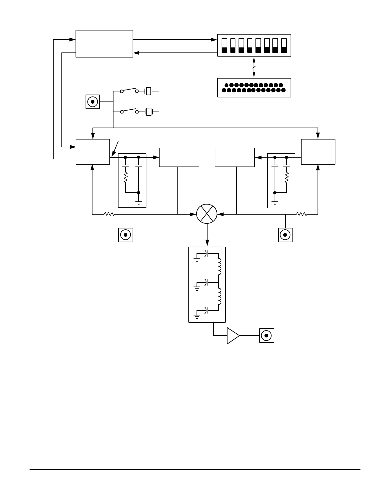
Frequency
Control Data
External Reference
Out A, Out B,
Lock Detect
74HCT241, 74LS126
Buffer Logic
PD
out
MC145220
PLL
F
in
Loop Filter
10.01 MHz TCXO
14.4 MHz TCXO
VCO
733 – 743 MHz
REF
in
790 – 820 MHz
LO RF
Logic Control Switches
Parallel Port Connector
Loop Filter
VCO
′
MC145220
′
PLL
F
in
Single Loop Output
733–743 MHz
Figure 1. Evaluation Kit Block Diagram
IF
Single Loop Output
790 – 820 MHz
Fc = 80 MHz
Dual Mode Output
60 – 80 MHz
(f′ – f)
Amplifier
MC145220EVK
6
MOTOROLA
Page 7

TYPICAL PERFORMANCE
Typical performance applies only to the configuration as shipped. The MC145220EVK is shipped with
V+ = 5 V. For lowest phase noise in single or dual loop mode, a 50 Ω load must be connected to J12.
Single Loop PLL Single Loop PLL′ Dual Loop PLL
Supply Voltage (J8) 11.5 – 12.5 V
Supply Current (J8) (Note 1) 177 mA
Available Current (Note 2)
45 mA
Frequency Range (Note 3) 733 – 743 MHz 790 – 820 MHz 60 – 80 MHz
Reference Frequency (M1) 10.01 MHz
Temperature Stability
< ± 2.5 ppm
(M1, – 30°C to + 70°C)
Reference Frequency (M5) 14.4 MHz
Temperature Stability
< ± 2 ppm
N/A
N/A
(M5, – 30°C to + 85°C)
TCXO Aging (M1, M5) < ± 1 ppm / year
Step Size 10 kHz 10 Hz
Power Output
Frequency Accuracy
Reference Sidebands (Note 4)
Phase Noise (100 Hz)
Phase Noise (10 kHz) (Note 5)
Switching Time (Note 6)
NOTES:
1. Supply current is current the board requires without user modifications.
2. Available current is the sum of currents available to the user (in the prototype area) from the 5 V and 8.5 V supply. The 12 V supply is not
regulated. Current at 12 V is limited by the external power supply . If the on–board VCO and amplifier are disconnected from the power bus,
more current can be drawn in the prototype area. The current flowing into U5 (the 8.5 V regulator) should not exceed 180 mA. This will limit
temperature rise in U5.
3. Frequency ranges require use of the 5 V default charge pump supply voltage.
4. VCO sidebands on PLL at low step sizes (10 kHz) are limited by control line leakage of the VCO. Up to 24 nA of leakage has been seen.
At higher step sizes (100 kHz and above), this effect is much less noticable. This did not affect PLL′ because its VCO leakage was less than
10 pA.
5. 10 kHz phase noise is limited by the PLL device noise. For low noise designs, the loop bandwidth is made narrower and the VCO is relied
upon to provide the 10 kHz phase noise. This can be seen on the EVKs since the VCOs have much lower noise.
6. 10 MHz step, within ± 1 kHz of final frequency (’220).
Due to the software architecture, when the user is measuring the switching time of a single board in dual loop mode, it takes 20 ms to load
the data as compared to single loop mode, which takes 8 ms to load the data. This is a limitation of the software, not the IC.
To find the actual PLL switching time, subtract 8 or 20 ms from the switching time stated in the table.
– 3.0 dBm – 5.0 dBm
± 1.5 kHz ± 1.5 kHz
– 57 dB – 74 dB
– 65 dBc/Hz – 56 dBc/Hz
– 104 dBc/Hz – 90 dBc/Hz
24 ms 40 ms
4.5 – 7.5 dBm
± 50 Hz
– 57 dB
– 50 dBc/Hz
– 89 dBc/Hz
45 ms
MOTOROLA
MC145220EVK
7
Page 8

SUPPORT MATERIAL
The following documents are included in the appendix:
1. Schematic diagram of MC145220EVK.
2. Bill of materials.
3. Parts layout diagram.
4. Mechanical drawing of board.
5. MC145220 data sheet.
6. Typical signal plots.
PRODUCTION TEST
After assembly is complete, the following alignment and test is performed:
1. The control program is started in ’220 single loop mode.
2. [L]! is selected to set PLL frequency to 733 MHz.
3. Power is applied to the board. DIP switch section 1 is closed circuit with all others being open
circuit.
4. After attaching computer cable, [I]! is selected.
5. Trim resistor VR1 is adjusted to obtain an output frequency at J5 of 733 MHz ± 500 Hz.
6. Voltage at the control voltage test point (TP2) is measured. It must be > 0.5 V.
7. [H]! is selected.
8. Voltage at the control voltage test point (TP2) is measured. It must be < 4.4 V.
9. [T]! is selected to toggle to PLL′.
10. [L]! is selected to set PLL′ frequency to 790 MHz.
11. Voltage at the control voltage test point (TP9) is measured. It must be > 0.5 V.
12. [H]! is selected to set PLL′ frequency to 820 MHz.
13. Voltage at the control voltage test point (TP9) is measured. It must be < 4.4 V.
14. [G] is selected and the board type is changed to ’220 dual loop mode.
15. [Q]!, then [I]!, is selected to initialize the dual mode output (J12) to 70 MHz. The frequency should
be 70 MHz ± 50 Hz.
If in step 5 it isn’t possible to obtain a signal on frequency , the adjustment screw in M1 may be turned for
further frequency adjustment range. If neither adjustment works, [P] should be selected and the correct
printer port address entered. [I]! is then selected to reload the data.
BOARD OPERATION
A computer is connected to the DB–25 connector J9. Data is output from the printer port. The printer card
is in slot 0 using the default address in the control program. Data is sent to the PLL device (U1) through
the DIP switch (S1), and 74HCT241 buffer (U2). D1, D2, D3, R7, R8, and R12 are in the data path between the ’HCT241 and PLL device. This limits the high level output voltage of the buffer . V oltage on PLL
device inputs must be no greater than 0.5 V above V+. A ’220 PLL has three output lines which are
routed through a 74LS126 line driver (U3) back to the computer.
U2, the 74HCT241, provides isolation and logic translation for PLL input lines. Logic translation is needed from the TTL levels on the printer port to the CMOS levels on the ’220 inputs.
A 12 V power supply should be used to power the board at J8 (Augat 2SV–02 connector). The 2SV–02
will accept 18–24 AWG bare copper power leads. No tools are needed for connection. If power is properly connected, LED D4 will be lit.
MC145220EVK
8
MOTOROLA
Page 9
Power passes from J8 to U5 (LM317 regulator) configured as an 8.5 V regulator. 8.5 V powers the VCOs.
Regulators U6 and U7 use the 8.5 V supply to produce 3 V and 5 V. The ’220 board can use either to
power the logic and charge pump. V+ voltage is selected by J11. U6 and U7 are cascaded with U5 to
equalize their individual voltage drops.
The ’220 operates in both a single loop and dual loop mode. There are no component changes between
the two modes. The differences are in the programming of the counters and the SMA connector that is
used.
The PLL loop is composed of the MC145220 (U1), 733 – 743 MHz VCO (M2), and a passive loop filter
(R4, R5, C6, C7, C8). In single loop mode, output is taken from J5. A passive loop filter was used to keep
the design simple, reduce noise, and reduce the quantity of traces susceptible to stray pickup. The PLL′
loop is composed of the MC145220 (U1), 790 – 820 MHz VCO (M3), and a passive loop filter (R22, R25,
C24, C26, C30). In single loop mode, output is taken from J10.
Dual mode output is the (f′ – f) frequency output from the mixer. It is low pass filtered (L1, L2, C15, C21,
C22) then amplified (U4). The output is available at J12.
Phase detector current is 2 mA. J1 is a removable jumper used for current measurement of V+.
Two TCXOs, a Motorola Saber 14.4 MHz (M5), and Raltron 10.01 MHz (M1) are supplied. As shipped
from the factory, the 10.01 MHz TCXO is in use. This allows both the 10 kHz and 10 Hz step sizes to be
used with one TCXO. 10.01 MHz cannot be divided for larger step sizes such as 100 kHz. For larger step
sizes use the Saber. Jumpers J3, J4, J13, and J14 determine which TCXO or the external reference
input is in use.
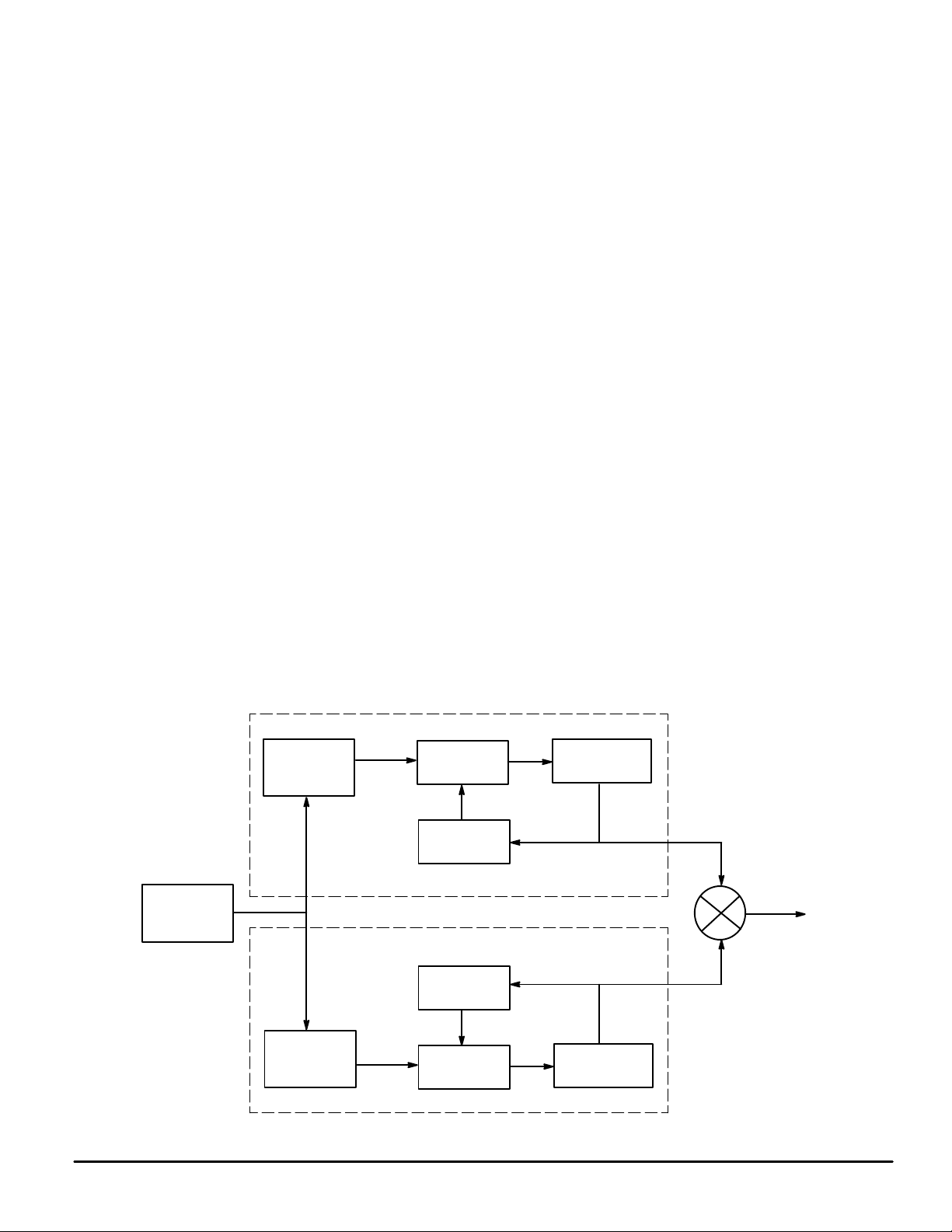
DUAL MODE OUTPUT
The dual mode output (J12) is the difference frequency from mixing PLL and PLL′. By using a reference
frequency of 10.01 MHz, PLL can be operated with a 10.01 kHz step size and PLL′ with a 10 kHz step
size. If both PLL and PLL′ step down in frequency , the mixed output will step up by 10 Hz. More information on the offset reference technique is in AN1277/D, Offset Reference PLLs for Fine Resolution or
Fast Hopping. The block diagram, formulas, and an example are shown in Figure 2.
REFERENCE
10.01 MHz
R COUNTER
÷
1000
10.01 kHz
PLL
PLL
N = 73,001 – 74,000
N
′
′
PHASE
DETECTOR
÷
N
COUNTER
= 79,075 – 82,074
÷
N
′
COUNTER
VCO
730.7 – 740.7 MHz
MIXER
f
f
′
(f
′ – f)
60 – 80 MHz
(10 Hz STEPS)
MOTOROLA
R′ COUNTER
÷
1001
Figure 2. Dual Mode Block Diagram
10 kHz
PHASE
DETECTOR
VCO
790.7 – 820.7 MHz
MC145220EVK
9
Page 10
PLL PLL′
f = N (10.01 kHz) f′ = N′ (10 kHz)
f = 10.01 kHz 74,000 –
N = 74,000 –
r(f′ – f)
10 Hz
r(f′ – f)
10 Hz
f′ = 10 kHz
N′ = N + 74 +
w(f′ – f) + 740 kHz
10 kHz
w(f′ – f)
10 kHz
(f′ – f) = w(f′ – f) + r(f′ – f)
(f′ – f) = Desired Output Frequency
w(f′ – f) = Output Frequency Portion that Divides Evenly by 10 kHz
r(f′ – f) = Remainder from Output Frequency Division by 10 kHz
Dual Mode Formulas
Example: Synthesize 76.849 930 MHz
r(f′ – f) = 9.930 kHz, w(f′ – f) = 76.840 MHz
N = 74,000 –
9.930 kHz
= 73,007
f = 73,007 (10.01 kHz) = 730.800 070 MHz
10 Hz
+ N
N ′= 73,007 + 74 +
76.840 MHz
= 80,765
f′ = 80,765 (10 kHz) = 807.650 000 MHz
10 kHz
(f′ – f)= 807.650 000 MHz – 730.800 070 MHz = 76.849 930 MHz
MC145220EVK
10
MOTOROLA
Page 11

EXTERNAL REFERENCE INPUT
To use an external reference, disconnect J3, J4, J13, and J14. Use a reference signal at J2 which complies with data sheet requirements. Then modify the reference frequency in the program main menu to
reflect the changes made (F menu item).
DATA TRANSFER FROM COMPUTER TO EVK
To control the serial input EVK with the parallel printer port, a conversion is done. Printer cards are designed to output eight bits through eight lines. A bit mask is used to obtain the bit combination for the
three required output lines (Data, Clock, Load). As bytes are sent to the printer card in sequence, it appears to be a serial transfer. The printer port is used because data transfer using the serial port would be
much slower. A standard IBM PC can support a parallel port data rate of 4.77 MHz.
IBM PCs and compatibles can accept up to three printer port configurations. These ports are called
LPT1, LPT2, and LPT3. Each printer port has a unique address. Two sets of addresses are in common
use. One set applies to IBM PC XT, AT, and clones. The other is for the PS 2 line. To load data into the
EVK, the correct address must be selected. The program default is $278. If $278 is not the address in
use, it must be modified by entering the P menu item in the main menu. All allowed addresses given in
hexadecimal are as follows:
Label
IBM PC and Clones PS 2
LPT1 278 3BC
LPT2 378 378
LPT3 3BC 278
Up to three EVK boards can operate independently from one printer port. All lines on the printer port are
connected to every EVK. Even with three boards operating, only three output lines (Clock, Data, and
Load) from the printer card are used. If two boards are controlled together, data for the second board is
received from the Output A of the first. Output A is a configurable output on ’220 devices, which in this
case is used to shift data through chip 1 into chip 2. Output A and Data are connected using a printer port
input line. This was done to avoid connecting extra wires. Fortunately not all port input lines are needed
for computer input. Load and Clock are common to both boards.
A three–board cascade is handled similarly to a two–board cascade. Out A on the first board is fed to
Data on the second. Out A on the second connects to Data on the third. Instructing the program on the
quantity of boards connected together allows it to modify the number of bits sent.
All boards have a DIP switch S1 which gives each a unique address. The configuration menu is used to
tell the program what type of board is connected at a board address. Switch positions for all possible
addresses are given in Figure 3.
MOTOROLA
MC145220EVK
11
Page 12
Single Board Operation
Closed
Open
Closed
Open
Closed
Open
12345678
T wo– or Three–Board Cascade
Board A
12345678
Board B
12345678
Board C
12345678
Closed
Open
Figure 3. Switch Positions
In Figure 3, DIP switch sections 6, 7, and 8 allow the computer to read Out A, Lock Detect′, or Lock
Detect from the PLL device. Each of the inputs can only be read on one board at a time, but each item
could be read on a different board. In a three–board cascade, Out A could be read from the first board,
Out B from the second, and Lock Detect from the third. There is no way to determine the board address
of a particular input with software. The control program does not make use of these inputs; however,
source code could be modified as required. Pin assignment on the printer port connector is:
Label
Pin Number
Out A 12
Out B 13
Lock Detect 15
MC145220EVK
12
MOTOROLA
Page 13
PRINTER PORT CONFIGURATION
Printer port outputs on an IBM PC or clone use TTL–LS logic levels. Inputs are one TTL–LS load. Signal
lines can be used for any purpose. The standard names, direction of data flow, true and inverted data are
shown in Figure 4.
Printer
Signal Name
– Strobe
+ Data Bit 0
+ Data Bit 1
+ Data Bit 2
+ Data Bit 3
+ Data Bit 4
+ Data Bit 5
+ Data Bit 6
+ Data Bit 7
– Acknowledge
+ Busy
+ P. End (out of paper)
+ Select
– Auto Feed
– Error
– Initialize Printer
– Select Input
Ground
Pin Number
1
2
3
4
5
6
7
8
9
10
11
12
13
14
15
16
17
18 – 25
IBM Printer
Port
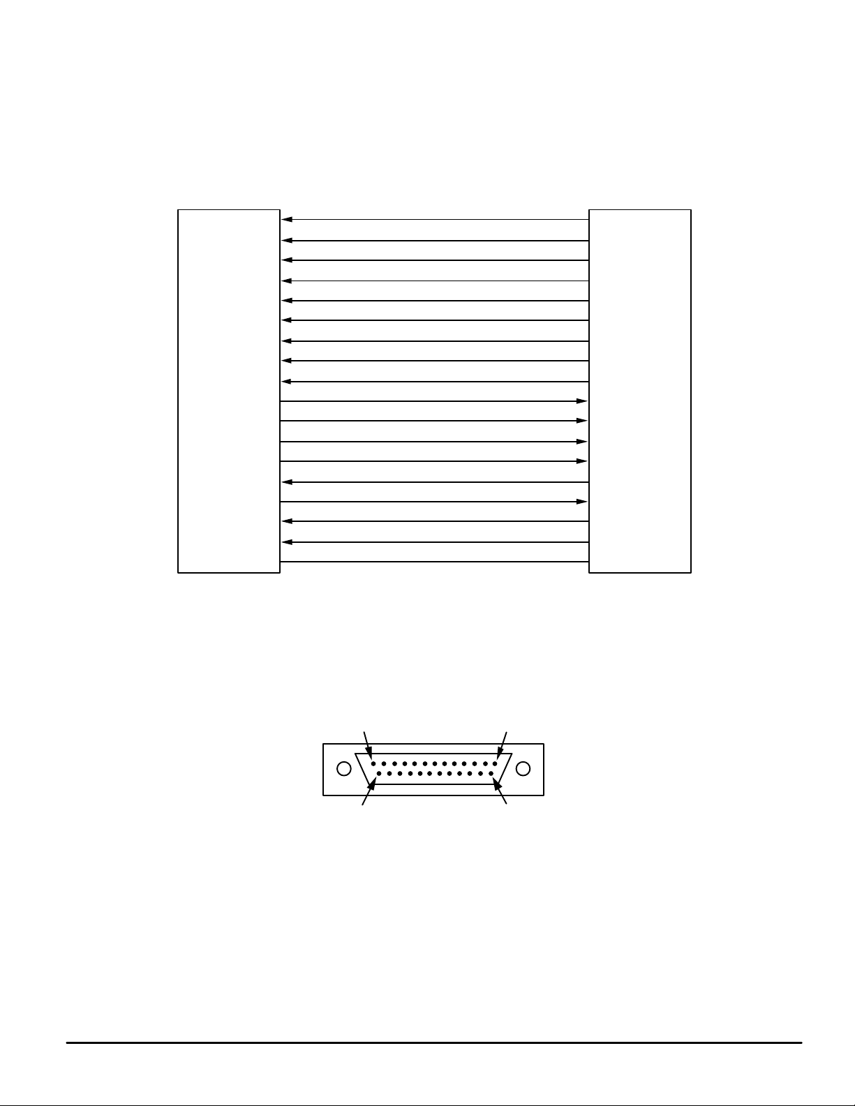
Figure 4. Printer Port Data Lines
Pin numbers for the port connector are shown in Figure 5.
13
25
(front view)
Figure 5. DB–25 Male Connector
1
14
MOTOROLA
MC145220EVK
13
Page 14
SECTION 2 – SOFTWARE DESCRIPTIONS
Á
Á
INTRODUCTION
The MC145xxx PLL software is provided to demonstrate the capabilities of the MC145xxx family of PLLs.
The family includes the following devices:
Table 1.
PURPOSE
БББББББББББ
БББББББББББ
Board Type
MC145190
MC145191
MC145192
MC145200
MC145201
MC145202
MC145220 in Single Loop Mode
MC145220 in Dual Loop Mode
Board Description
ББББББББББ
ББББББББББ
Low voltage version of the ’191
Low voltage version of the ’201
The user guide for the MC145xxx PLL software familiarizes the user with the use and capabilities of the
program referred from here on as PLLDEMO Version 4.0. The guide covers the user interface and a
summary of the commands that are available.
The user should read the data sheet of the PLL frequency synthesizer of interest before using the software.
DESCRIPTION
The PLL software:
• is a Pascal program developed with Borland Turbo Pascal v7.0.
• runs under MS–DOS.
• is a character–based, menu–driven program.
USER INTERFACE
The user interface consists of numerous character–based, menu–driven screens which are displayed
below. Each screen is shown, along with a description of its purpose. Note that all screen shots shown
are a representative sample of the program. They are provided to familiarize the end user with the program.
INSTALL
To install this program, create a directory called “PLLEVAL”. Change directories into “PLLEVAL” and
copy PLL.exe into this directory.
MC145220EVK
14
MOTOROLA
Page 15

UNINSTALL
To uninstall this program, change directories into “PLLEVAL” and type “erase*.*”. After this command,
change out of directory “PLLEVAL” and type “erase PLLEVAL”.
Note: If you are in Windows 3.X or Windows 95, this program adds no entries into .ini or Registry files.
It is recommended that you have the PLL program running while you are reviewing this manual. Due to
the number of screens that may be involved in your evaluation, following the connections, screens, and
commands is easier when the manual and program are used together.
CONVENTIONS
Some of the PLLDEMO screens are necessarily “busy”. Because of this, the program follows several
conventions to help the user quickly absorb the screen information. These conventions are briefly described on a help screen that is available throughout the program. Type the help command, [?], at any
time to view the help screen.
The conventions are as follows:
1. Command keys are surrounded by [ ]s. Type the letter between the [ ]s to execute the command.
[ ]s are followed by a description of the command.
2. [–] indicates a command not available to the user. Commands become available when they are
applicable to the currently targeted board.
3. [ ]s followed by an ! indicate the command will execute immediately. Otherwise a submenu is displayed from which further choices may be made.
4. If no changes are desired to an input field, leave the field blank. The previous value will then be used
for that field. Type the T AB key to move to the next input field, or shift–T AB to move to the prior input
field. Type RETURN to store the new input values while remaining on the same screen. Type Q to
store the new values and return to the prior screen.
5. All numbers are entered as decimal values unless otherwise noted. A $ followed by a value indicates
the value is in hexadecimal format. The output port address is in hexadecimal format.
6. The second line from the top of screen (screen title) states the purpose of the screen.
7. Screen information that can be changed by the user is displayed in bold or reverse video.
8. Commands are case independent. X is the same as x.
9. Frequencies are entered as two numbers, and displayed as one. The two input numbers represent
the desired frequency in MHz, and in kHz. These input values are added together to obtain the final
frequency. Leave either input field blank to retain the prior value for that portion of frequency.
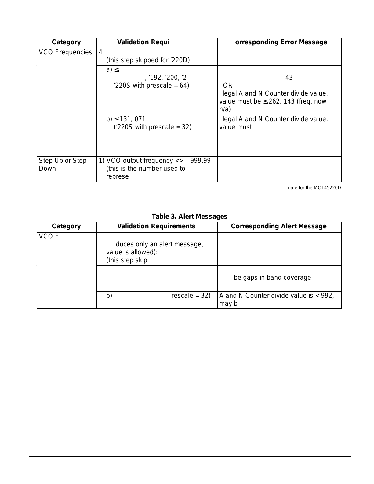
ALERT AND ERROR MESSAGES
This program contains two types of messages that appear when conditions warrant. (See Table 2.)
1. Alert Messages. These messages alert you that though the current values are valid, you are unable
to continuously increment the A and N counters. Hit any key to remove these messages and continue with the program. There are some instances of the alert messages where you may have to hit
any key twice to remove the message.
2. Error Messages. These are messages that indicate you have selected conditions that are outside
of the valid parameters of the IC. After hitting any key to continue, the invalid parameters you selected will change back to the default parameters of the program. Y ou may then enter another value
to continue your evaluation. There are some error messages where you may have to hit any key
twice to remove the message.
MOTOROLA
MC145220EVK
15
Page 16
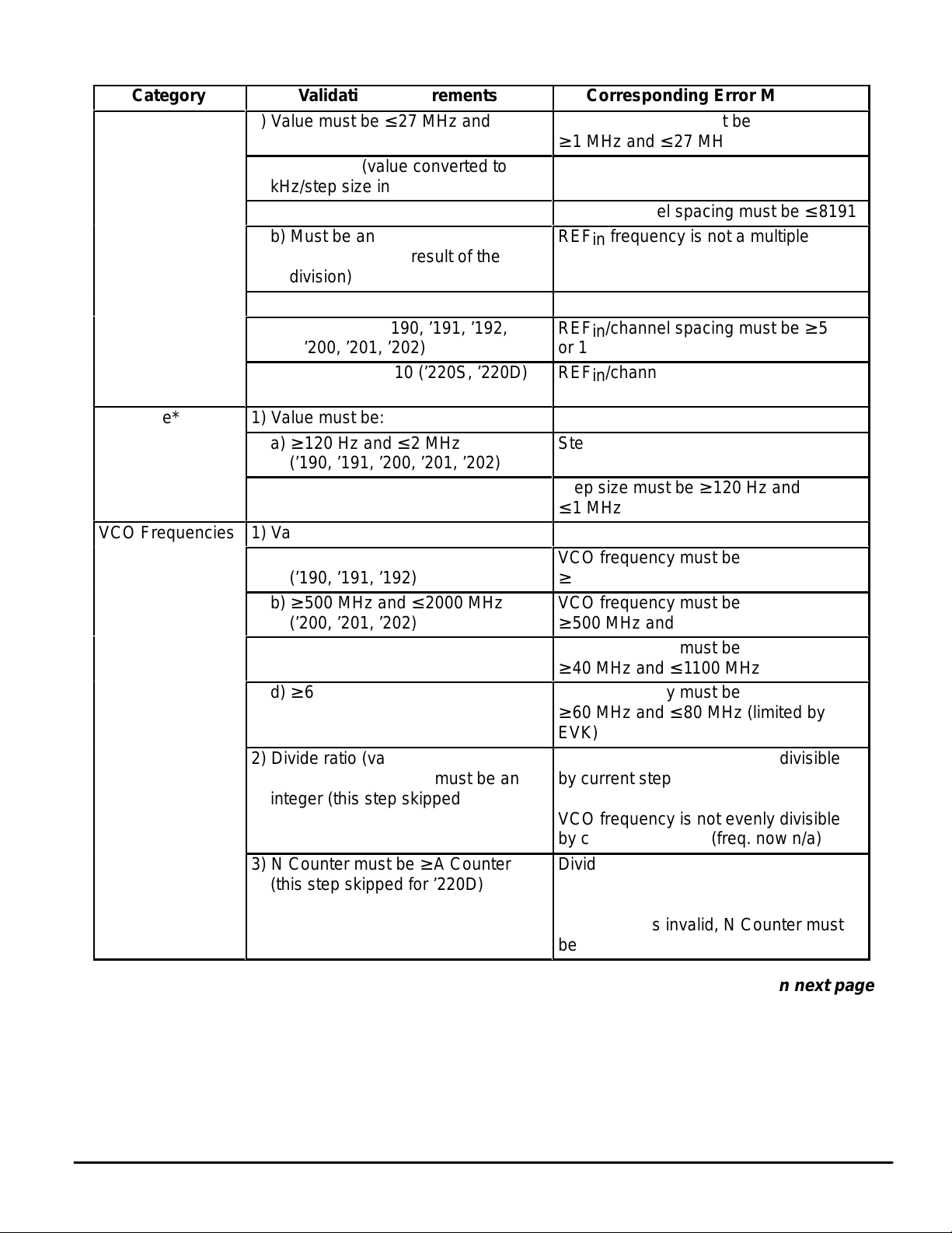
Table 2. Error Messages
Á
Á
Á
Á
Á
Á
Á
Á
Á
Á
Á
Á
Á
Á
Á
Á
Á
Á
Á
Á
Á
Á
Á
Á
Á
Á
Á
Á
Á
Á
Á
Á
Á
Á
Á
Á
Á
Á
Á
Á
Á
Á
Á
Á
Á
Á
Á
Á
Á
Á
Á
Á
Á
Category
REFin Frequency*
ББББББ
1) Value must be ≤ 27 MHz and
Validation Requirements
ББББББББББББ
≥ 1 MHz
2) Divide ratio (value converted to
ББББББÁББББББББББББ
kHz/step size in kHz):
a) Must be ≤ 8191
b) Must be an integer (there must
ББББББ
ББББББ
ББББББББББББ
be no fractional result of the
division)
ББББББББББББ
c) Must be in range:
i) = 1 or ≥ 5 (’190, ’191, ’192,
ББББББÁББББББББББББ
’200, ’201, ’202)
ii) = 1 or be ≥ 10 (’220S, ’220D)
ББББББÁББББББББББББ
Step Size*
ББББББ
1) Value must be:
ББББББББББББ
a) ≥ 120 Hz and ≤ 2 MHz
ББББББ
ББББББÁББББББББББББ
(’190, ’191, ’200, ’201, ’202)
ББББББББББББ
b) ≥ 120 Hz and ≤ 1 MHz
(’192, ’220S, ’220D)
VCO Frequencies
ББББББÁББББББББББББ
ББББББÁББББББББББББ
1) Value must be:
a) ≥ 100 MHz and ≤ 1100 MHz
(’190, ’191, ’192)
b) ≥ 500 MHz and ≤ 2000 MHz
(’200, ’201, ’202)
c) ≥ 40 MHz and ≤ 1100 MHz
ББББББÁББББББББББББ
(’220S)
d) ≥ 60 MHz and ≤ 80 MHz (’220D)
ББББББ
ББББББ
ББББББББББББ
ББББББББББББ
2) Divide ratio (value converted to
ББББББ
ББББББ
ББББББ
kHz/step size in kHz) must be an
ББББББББББББ
integer (this step skipped for ’220D)
ББББББББББББ
ББББББББББББ
3) N Counter must be ≥ A Counter
ББББББ
ББББББ
ББББББ
ББББББ
ББББББББББББ
(this step skipped for ’220D)
ББББББББББББ
ББББББББББББ
ББББББББББББ
Corresponding Error Message
REFin frequency must be
ББББББББББББ
≥ 1 MHz and ≤ 27 MHz
ББББББББББББ
REFin/channel spacing must be ≤ 8191
REFin frequency is not a multiple of the
ББББББББББББ
step size
ББББББББББББ
REFin/channel spacing must be ≥ 5
or 1
ББББББББББББ
REFin/channel spacing must be ≥ 10
or 1
ББББББББББББ
ББББББББББББ
Step size must be ≥ 120 Hz and
≤ 2 MHz
ББББББББББББ
Step size must be ≥ 120 Hz and
ББББББББББББ
≤ 1 MHz
VCO frequency must be
ББББББББББББ
≥ 100 MHz and ≤ 1100 MHz
VCO frequency must be
ББББББББББББ
≥ 500 MHz and ≤ 2000 MHz
VCO frequency must be
ББББББББББББ
≥ 40 MHz and ≤ 1100 MHz
VCO frequency must be
ББББББББББББ
≥ 60 MHz and ≤ 80 MHz (limited by
EVK)
ББББББББББББ
VCO frequency is not evenly divisible
by current step size
ББББББББББББ
–OR–
ББББББББББББ
VCO frequency is not evenly divisible
ББББББББББББ
by current step size (freq. now n/a)
Divide ratio is invalid, N Counter must
ББББББББББББ
be ≥ A Counter
ББББББББББББ
–OR–
Divide ratio is invalid, N Counter must
ББББББББББББ
be ≥ A Counter (freq. now n/a)
ББББББББББББ
MC145220EVK
16
Continued on next page
MOTOROLA
Page 17
Continued from previous page
Á
Á
Á
Á
Á
Á
Á
Á
Á
Á
Á
Á
Á
Á
Á
Á
Á
Á
Á
Á
Á
Á
Á
Á
Á
Á
Á
Á
Á
Á
Á
Á
Á
Á
Á
Á
Á
Á
Á
Á
Á
Á
Á
Á
Á
Á
Á
Á
Á
Á
Á
Category
ББББББ
VCO Frequencies
ББББББ
ББББББ
ББББББ
ББББББ
ББББББ
ББББББ
ББББББ
ББББББ
ББББББ
Step Up or Step
ББББББ
Down
ББББББ
4) Divide ratio must be:
(this step skipped for ’220D)
a) ≤ 262,143
(’190, ’191, ’192, ’200, ’201, ’202,
’220S with prescale = 64)
b) ≤ 131, 071
(’220S with prescale = 32)
1) VCO output frequency <> – 999.99
(this is the number used to
represent n/a)
Validation Requirements
ББББББББББББ
ББББББББББББ
ББББББББББББ
ББББББББББББ
ББББББББББББ
ББББББББББББ
ББББББББББББ
ББББББББББББ
ББББББББББББ
ББББББББББББ
ББББББББББББ
ББББББББББББ
Corresponding Error Message
ББББББББББББ
ББББББББББББ
Illegal A and N Counter divide value,
ББББББББББББ
value must be ≤ 262,143
ББББББББББББ
–OR–
ББББББББББББ
Illegal A and N Counter divide value,
ББББББББББББ
value must be ≤ 262, 143 (freq. now
n/a)
ББББББББББББ
Illegal A and N Counter divide value,
value must be ≤ 131,071
ББББББББББББ
–OR–
ББББББББББББ
Illegal A and N Counter divide value,
ББББББББББББ
value must be ≤ 131.071 (freq. now n/a)
VCO frequency is invalid
ББББББББББББ
ББББББББББББ
*NOTE: REFin and step size are NOT validated on the ’220D board. These validation sequences may not be appropriate for the MC145220D.
Table 3. Alert Messages
Category
VCO Frequencies
ББББББ
ББББББ
ББББББ
ББББББ
ББББББ
ББББББ
ББББББ
1) Divide ratio must be (violation
produces only an alert message,
value is allowed):
(this step skipped for ’220D)
a) ≥ 4032
(’190, ’191, ’192, ’200, ’201,
’220S with prescale = 64)
b) ≥ 992 (’220S with prescale = 32)
Validation Requirements
ББББББББББББ
ББББББББББББ
ББББББББББББ
ББББББББББББ
ББББББББББББ
ББББББББББББ
ББББББББББББ
Corresponding Alert Message
ББББББББББББ
ББББББББББББ
ББББББББББББ
A and N Counter divide value is < 4032,
may be gaps in band coverage
ББББББББББББ
ББББББББББББ
A and N Counter divide value is < 992,
ББББББББББББ
may be gaps in band coverage
ББББББББББББ
MOTOROLA
MC145220EVK
17
Page 18

SCREENS
‘Define boards to program’
The first screen the user sees when the program begins has a screen title of ‘Define boards to program’.
This screen is used to define which boards are connected to the LPT1 printer port of the computer. Refer
to the hardware setup section to determine how to cascade the evaluation boards.
This screen is also available from the main menu. The user may return to this screen by depressing [Q]
to change the boards that are connected to the computer.
The screen is divided into two sections. The upper section shows the current board type settings while
the lower section allows the user to define a board’s type and position in the cascade connection.
Notice the section labeled ‘Available Boards:’ shows three labels, one for each board that may be cascaded. When the program first starts up it shows ‘N/A’ (not applicable) after each label. The user must
enter the boards contiguously. Initially the program requests for the user to enter board A’s type. This is
signified by
typing the corresponding command.
A
(in the screen below) being set to A. The user can the select the board type for board A by
Once board A’s type is selected,
A
automatically increments to B and the process may be repeated.
Once all boards have been correctly defined, the user may select [Q] which sends default data to the
boards and continues to the next screen. NOTE: Before selecting [Q], the user should insure that the
DIP switch settings shown in Figure 2 are correct.
If a board is incorrectly identified, select the board that is not correctly defined by typing the corresponding board letter ([A], [B], or [C]). The user may then reselect the board’s type. Once the board has been
identified, the user may select the letter ([A], [B], or [C]) of the board followed by [S] to change hardware–
dependent variables for that board.
[X] can be selected to exit the program completely. [?] can be selected to view the help screen.
Welcome to MC145xxx EVK Demonstration Program, rev 4.0
Define boards to program
Available Boards:
Brd [A]!: N/A Brd [B]!: N/A Brd [C]!: N/A
––––––––––––––––––––––––––––––––––––––––––––––––––––––––––––––––––––––––––––––––
Board
[–]! no board [5]! MC145201
[1]! MC145190 [6]! MC145202
[2]! MC145191 [7]! MC145220 Single
[3]! MC145192 [8]! MC145220 Dual
[4]! MC145200
A
is:
[–] Boards defined, Continue
MC145220EVK
18
[X]! Terminate demonstration program. [?]! View help screen.
MOTOROLA
Page 19

Help Screen
This is the help screen for the program. It is available from any point throughout the program. A short list
of the interface conventions are presented on this screen.
[X] can be selected to exit the program completely. [Q] can be selected to exit the help screen.
Welcome to MC145xxx EVK Demonstration Program, rev 4.0
1) Command keys are surrounded by []’s. Type the letter between the []’s to execute
the command. []’s are followed by a description of the command.
2) [–] indicates a command not available to the user.
3) []’s followed by an ! indicate the command will execute immediately. Otherwise a
sub menu will be displayed.
4) If no changes are desired to an input field, type the TAB key to move to the next
input field. The previous value will be used for that field.
5) All numbers are entered as decimal values unless otherwise noted. A $ followed by a
value indicates the value is in hexadecimal format.
6) The second line from the top of screen (screen title) states the purpose of the
screen.
7) Screen information that can be changed by the user is displayed in bold or reverse
video.
8) Commands are case independent. X is the same as x.
[X]! Terminate demonstration program. [Q]! Quit help screen.
To access this screen, press shift + ? on your keyboard while within any screen in the program.
MOTOROLA
MC145220EVK
19
Page 20

‘Select from the available options’
This is the main screen of the program. This is where the user enters commands to demonstrate the
capabilities of the various boards connected to the computer. The title of the screen is ‘Select from the
available options’.
This screen is broken down into three sections:
‘Available Boards’
This section displays the board types that are connected to the computer. It also designates which
board is the currently selected ‘target’ board. This is the board that will receive the commands from
‘MC145xxx Commands’ section. This section also provides the ability to change the targeted
board. Type the target board command ([A], [B], or [C]) to target that particular board.
‘MC145xxx Commands’
This section is further divided into three subsections. Each subsection contains commands that can
be sent to the ‘target’ board to demonstrate its capabilities. Each of these commands is described in
full in the Command Summary.
The first subsection, ‘MC145xxx Frequency Commands’, contains commands that are
used to modify the PLL frequency in some way . These commands are available for all possible target board types.
In the top line of this section, ‘Current Output Frequency is
70 MHz’
designates what the
frequency is for the currently targeted board. This value is dynamic.
On the lines below this,
70 MHz
is the current setting for the default medium frequency .
60 MHz
is the current setting for the default low frequency.
80 MHz is
the current setting
for the default high frequency.
The second subsection, ‘MC145xxx Additional Commands’, contains commands that
are used to further modify the currently targeted board. These commands also work with all
of the MC145xxx board types.
The third subsection, ‘MC145220 EVK – Single Specific Commands’, are only displayed when the MC145220EVK in single loop mode is the currently targeted board. This
section shows commands that are specific to this board. This is required since this board
contains the equivalent of two PLLs.
The command letter for ‘Set target PLL on board’ is [T]!. In single loop mode, the user may
toggle between PLL and PLL′ on the MC145220EVK by using this command. Feedback is
given to the user as to whether PLL or PLL′ will be accessed. See near the top of the screen
on the line titled “Available Boards - Current target board is: ...”
‘Initialization/System Setup Commands’
This section contains commands that are used to initialize all boards connected to the computer or
to set up the computer.
MC145220EVK
20
MOTOROLA
Page 21

‘Select from the available options’ (continued)
Welcome to MC145xxx EVK Demonstration Program, rev 4.0
Select from the available options
Available Boards – Current target board is: A, MC145220 Dual
Brd [A]!: MC145220 Dual Brd [–]!: N/A Brd [–]!: N/A
––––––––––––––––––––––––––––––––––––––––––––––––––––––––––––––––––––––––––––––––
MC145xxx Frequency Commands – Current Output Frequency is
[L]! Set to low freq.
[M]! Set to med. freq.
[H]! Set to high freq.
[U]! Step frequency up by step size [O] Set PLL output frequency
[D]! Step frequency down by step size [F] REFin freq. & channel spacing
MC145xxx Additional Commands
[E] Set function of output A [N] Change C register and Prescale
[R] Set crystal/reference mode – Current mode is Ref. mode, REFout low
––––––––––––––––––––––––––––––––––––––––––––––––––––––––––––––––––––––––––––––––
Initialization/System Setup Commands:
[P] Set output port address – Current address is $278
[G] Change board definitions
[I] Initialize board(s), Write all registers
[X]! Terminate demonstration program. [?]! View help screen.
60 MHz
70 MHz
80 MHz
[W] Change default low freq.
[Y] Change default med. freq.
[Z] Change default high freq.
70 MHz
This screen shot is a representative sample of the screens within this program. To access this screen
with the MC145220 Dual EVK selected in the “Define boards to program” screen, press [Q]! . This will
place you in the “Select from the available options” screen you see above.
This sequence to access the “Select from the available options” screen works the same for any selected
board in the “Define boards to program” screen.
MOTOROLA
MC145220EVK
21
Page 22

PLL Output Frequency
This is the resulting screen that is displayed after the user selects the ‘[O] Set PLL output frequency’
command. The user is prompted to enter the new frequency.
The current output frequency is automatically retained if the user hits return or [Q] without entering a
value.
Welcome to MC145xxx EVK Demonstration Program, rev 4.0
Set PLL output frequency
Available Boards – Current target board is: A, MC145220 Dual
Brd [A]!: MC145220 Dual Brd [–]!: N/A Brd [–]!: N/A
––––––––––––––––––––––––––––––––––––––––––––––––––––––––––––––––––––––––––––––––
Input new frequency in integer values of MHz, kHz, and Hz.
Original program default PLL output frequency is 70 MHz
Current PLL output frequency is 70 MHz
Original program default frequency range is 60 MHz to 80 MHz
Current frequency range is 60 MHz to 80 MHz
Frequencies outside the program default frequency range will NOT be accepted.
New PLL frequency: 70 MHz + 000 kHz + 000 Hz
[TAB] to move to next field
[Q] to return to main menu
[X]! Terminate demonstration program. [?]! View help screen.
This screen shot is a representative sample of the screens within this program. To access this screen
with the MC145220 Dual EVK selected in the “Define boards to program” screen, press [Q]! . This will
place you in the “Select from the available options” screen. To access the screen shown above, press
[O].
This sequence to access the “Set PLL output frequency” screen works the same for any selected board
in the “Define boards to program” screen.
MC145220EVK
22
MOTOROLA
Page 23

REFin Frequency and Channel Spacing
This is the resulting screen that is displayed after the user selects the ‘[F] Set REFin freq. and channel
spacing’ command. The user is prompted to enter the new REFin frequency and channel spacing values,
or leave the fields blank to retain the prior settings. In ’220 dual mode, the user does not have the option
of changing REFin frequency or channel spacing.
Welcome to MC145xxx EVK Demonstration Program, rev 4.0
REFin frequency and channel spacing
Available Boards – Current target board is: A, MC145220 Dual
Brd [A]!: MC145220 Dual Brd [–]!: N/A Brd [–]!: N/A
––––––––––––––––––––––––––––––––––––––––––––––––––––––––––––––––––––––––––––––––
Due to the complexity of error checking in Dual Mode,
REFin frequency may not be modified.
The REFin frequency is 10.01 MHz
Due to the complexity of error checking in Dual Mode,
channel spacing may not be modified.
The channel spacing is 10 Hz
[Q] to return to main menu
[X]! Terminate demonstration program. [?]! View help screen.
This screen shot is a representative sample of the screens within this program. To access this screen
with the MC145220 Dual EVK selected in the “Define boards to program” screen, press [Q]! . This will
place you in the “Select from the available options” screen. To access the screen shown above, press [F].
This sequence to access the “REFin frequency and channel spacing” screen works the same for any
selected board in the “Define boards to program” screen.
MOTOROLA
MC145220EVK
23
Page 24

Set Default Low Frequency
This is the resulting screen that is displayed after the user selects the ‘[W] Change default low freq.’ command. The user is prompted to enter the new default low frequency value.
Entering a new value does not change the current output frequency of the target board. Changing the low
frequency simply adjusts the low frequency setting available from the main menu. The ‘[L]! Set to low
freq.’ command changes the current output frequency.
The screen is similar for the Y and Z commands except that the prompts specify medium or high frequency, respectively.
Welcome to MC145xxx EVK Demonstration Program, rev 4.0
Set default low frequency
Available Boards – Current target board is: A, MC145220 Dual
Brd [A]!: MC145220 Dual Brd [–]!: N/A Brd [–]!: N/A
––––––––––––––––––––––––––––––––––––––––––––––––––––––––––––––––––––––––––––––––
Input new default low frequency in integer values of MHz, kHz, and Hz.
Original program default low frequency is 60 MHz
Current low frequency is 60 MHz
New default low frequency: 60 MHz + 000 kHz + 000 Hz
[TAB] to move to next field
[Q] to return to main menu
[X]! Terminate demonstration program. [?]! View help screen.
This screen shot is a representative sample of the screens within this program. To access this screen
with the MC145220 Dual EVK selected in the “Define boards to program” screen, press [Q]! . This will
place you in the “Select from the available options” screen. To access the screen shown above, press
[W].
This sequence to access the “Set default low frequency” screen works the same for any selected board
in the “Define boards to program” screen.
MC145220EVK
24
MOTOROLA
Page 25

Set Function of Output A
This is the resulting screen that is displayed after the user selects the ‘[E] Set function of Output A’ command. The user is provided a submenu to select from.
The current setting for the function of Output A is displayed as Port, Data Out, fv or fr. The user may
choose from the listed commands to adjust this setting.
Welcome to MC145xxx EVK Demonstration Program, rev 4.0
Set function of Output A
Available Boards – Current target board is: A, MC145220 Dual
Brd [A]!: MC145220 Dual Brd [–]!: N/A Brd [–]!: N/A
––––––––––––––––––––––––––––––––––––––––––––––––––––––––––––––––––––––––––––––––
Set Output A function – Currently: Data Out
[0]! Port
[1]! Data Out
[2]! fv
[3]! fr
[Q] to return to main menu
[X]! Terminate demonstration program. [?]! View help screen.
This screen shot is a representative sample of the screens within this program. To access this screen
with the MC145220 Dual EVK selected in the “Define boards to program” screen, press [Q]! . This will
place you in the “Select from the available options” screen. To access the screen shown above, press
[E].
This sequence to access the “Set function of Output A” screen works the same for any selected board in
the “Define boards to program” screen.
MOTOROLA
MC145220EVK
25
Page 26

Change C Register and Prescale
This is the resulting screen that is displayed after the user selects the ‘[N] Change C Register and Prescale’ command. The user is provided a submenu to select from. Each submenu option also shows a
submenu. Note that in ’220 dual mode, some options are deleted. This is notated with the [–] symbol.
Welcome to MC145xxx EVK Demonstration Program, rev 4.0
Change C Register and Prescale
Available Boards – Current target board is: A, MC145220 Dual
Brd [A]!: MC145220 Dual Brd [–]!: N/A Brd [–]!: N/A
––––––––––––––––––––––––––––––––––––––––––––––––––––––––––––––––––––––––––––––––
Change C register:
[–] PDout Current Step Size
[–] Output B – (Out B)
[2] PDout Current – (PDout)
[3] Phase Detector Select – (PDA/B)
[–] Lock Detect Enable – (LDE)
[5] Phase Detector Polarity – (POL)
[6] Standby – (STBY)
Change Prescale:
[7] Prescale
[Q] to return to main menu
[X]! Terminate demonstration program. [?]! View help screen.
This screen shot is a representative sample of the screens within this program. To access this screen
with the MC145220 Dual EVK selected in the “Define boards to program” screen, press [Q]! . This will
place you in the “Select from the available options” screen. To access the screen shown above, press
[N].
MC145220EVK
26
MOTOROLA
Page 27

Change C Register, PD
Current
out
This is the resulting screen that is displayed after the user selects the ‘[N] Change C Register and Prescale’ and then the ‘[2] Change PD
This submenu contains commands to change the PD
Current’ command. The user is provided a submenu to select from.
out
current settings.
out
The screen is slightly different depending on whether Output A is defined as a port or not. See command
[E] from the main menu. Note in ’220 dual mode, PD
current for PLL and PLL′ is modified simulta-
out
neously by the software program.
The current PD
The user can select the [0], [1], [2], and [3] menu options to change the percent of PD
setting is displayed as ‘5%’, ‘50%’, ‘80%’, or ‘100%’.
out
out
If the [Q] command is selected, then the user is returned to the main menu.
Welcome to MC145xxx EVK Demonstration Program, rev 4.0
Change C Register, PDout Current
Available Boards – Current target board is: A, MC145220 Dual
Brd [A]!: MC145220 Dual Brd [–]!: N/A Brd [–]!: N/A
––––––––––––––––––––––––––––––––––––––––––––––––––––––––––––––––––––––––––––––––
Evaluation program modifies PDout Current on both PLL’s for this board.
Change C Register, PDout Current – Currently: 100%
[0]! 5%
[1]! 50%
[2]! 80%
[3]! 100%
[Q] to return to previous menu
current.
[X]! Terminate demonstration program. [?]! View help screen.
This screen shot is a representative sample of the screens within this program. To access this screen
with the MC145220 Dual EVK selected in the “Define boards to program” screen, press [Q]! . This will
place you in the “Select from the available options” screen. In this screen, press [N]. This will place you
in the “Change C Register and Prescale” screen. To access the screen above, press [2].
MOTOROLA
MC145220EVK
27
Page 28

Change C Register, Phase Detector Select
This is the resulting screen that is displayed after the user selects the ‘[N] Change C Register and Prescale’ and then the ‘[3] Change phase detector select’ command. The user is provided a submenu to select from. This submenu contains commands to toggle the phase detector setting.
The current phase detector setting is displayed as ‘phi R & phi V’ or ‘PD
’, depending on the setting.
out
The user can select the [0] and [1] menu options to toggle the phase detector select setting.
If the [Q] command is selected, then the user is returned to the main menu.
Welcome to MC145xxx EVK Demonstration Program, rev 4.0
Change C Register, Phase Detector Select
Available Boards – Current target board is: A, MC145220 Dual
Brd [A]!: MC145220 Dual Brd [–]!: N/A Brd [–]!: N/A
––––––––––––––––––––––––––––––––––––––––––––––––––––––––––––––––––––––––––––––––
Evaluation program modifies Phase Detector Select on both PLL’s for this board.
Change C Register, Phase Detector Select – Currently: PDout
[0]! phi R & phi V, phi R′ & phi V′
[1]! PDout, PDout′
[Q] to return to previous menu
[X]! Terminate demonstration program. [?]! View help screen.
This screen shot is a representative sample of the screens within this program. To access this screen
with the MC145220 Dual EVK selected in the “Define boards to program” screen, press [Q]! . This will
place you in the “Select from the available options” screen. In this screen, press [N]. This will place you
in the “Change C Register and Prescale” screen. To access the screen above, press [3].
This sequence to access the “Change C Register, Phase Detector Select” screen works the same for any
selected board in the “Define boards to program” screen.
MC145220EVK
28
MOTOROLA
Page 29

Change C Register, Polarity
This is the resulting screen that is displayed after the user selects the ‘[N] Change C Register and Prescale’ and then the ‘[5] Change polarity of phase detector’ command. The user is provided a submenu to
select from. This submenu contains commands to toggle the polarity setting.
The default ’220 dual setting of the polarity is displayed as ‘Non–invert PD
and PD
out
change phi R, R′ & phi V, V′ ’.
The user can select the [0] and [1] menu options to toggle the polarity setting.
If the [Q] command is selected, then the user is returned to the main menu.
Welcome to MC145xxx EVK Demonstration Program, rev 4.0
Change C Register, Polarity
Available Boards – Current target board is: A, MC145220 Dual
Brd [A]!: MC145220 Dual Brd [–]!: N/A Brd [–]!: N/A
––––––––––––––––––––––––––––––––––––––––––––––––––––––––––––––––––––––––––––––––
Evaluation program modifies Polarity on both PLL’s for this board.
Change C Register, Polarity – Currently: Non–invert PDout
[0]! Non–invert PDout and PDout′, do not interchange phi R, R′ & phi V, V′
[1]! Invert PDout and PDout′, interchange phi R, R′ & phi V, V′
[Q] to return to previous menu
′, do not inter-
out
[X]! Terminate demonstration program. [?]! View help screen.
This screen shot is a representative sample of the screens within this program. To access this screen
with the MC145220 Dual EVK selected in the “Define boards to program” screen, press [Q]! . This will
place you in the “Select from the available options” screen. In this screen, press [N]. This will place you
in the “Change C Register and Prescale” screen. To access the screen above, press [5].
This sequence to access the “Change C Register, Polarity” screen works the same for any selected
board in the “Define boards to program” screen.
MOTOROLA
MC145220EVK
29
Page 30

Change C Register, Standby
This is the resulting screen that is displayed after the user selects the ‘[N] Change C Register and Prescale’ and then the ‘[6] Change standby’ command. The user is provided a submenu to select from. This
submenu contains commands to toggle the standby state setting.
The standby state setting is displayed as ‘Normal operation’ or ‘Standby’, depending on the current setting.
The user can select the [0] and [1] menu options to toggle the standby state setting.
If the [Q] command is selected, then the user is returned to the main menu.
Welcome to MC145xxx EVK Demonstration Program, rev 4.0
Change C Register, Standby
Available Boards – Current target board is: A, MC145220 Dual
Brd [A]!: MC145220 Dual Brd [–]!: N/A Brd [–]!: N/A
––––––––––––––––––––––––––––––––––––––––––––––––––––––––––––––––––––––––––––––––
Evaluation program modifies Standby on both PLL’s for this board.
Change C Register, Standby – Currently: Normal Operation
[0]! Normal operation
[1]! Standby
[Q] to return to previous menu
[X]! Terminate demonstration program. [?]! View help screen.
This screen shot is a representative sample of the screens within this program. To access this screen
with the MC145220 Dual EVK selected in the “Define boards to program” screen, press [Q]! . This will
place you in the “Select from the available options” screen. In this screen, press [N]. This will place you
in the “Change C Register and Prescale” screen. To access the screen above, press [6].
This sequence to access the “Change C Register, Standby” screen works the same for any selected
board in the “Define boards to program” screen.
MC145220EVK
30
MOTOROLA
Page 31

Set Output Port Address
This is the resulting screen that is displayed after the user selects the ‘[P] Set output port address’ command. The user is prompted to enter the new output port address in hexadecimal. This should be the port
address of the LPT1 printer port for the user’s computer.
The original program default port address and the current setting are displayed.
Enter the new output port address in hexadecimal format.
Welcome to MC145xxx EVK Demonstration Program, rev 4.0
Set output port address
Available Boards – Current target board is: A, MC145220 Dual
Brd [A]!: MC145220 Dual Brd [–]!: N/A Brd [–]!: N/A
––––––––––––––––––––––––––––––––––––––––––––––––––––––––––––––––––––––––––––––––
Input new output port address in hexadecimal.
Original program default port address is $278
Current port address is $278
New output port address: $278
[Q] to return to main menu
[X]! Terminate demonstration program. [?]! View help screen.
This screen shot is a representative sample of the screens within this program. To access this screen
with the MC145220 Dual EVK selected in the “Define boards to program” screen, press [Q]! . This will
place you in the “Select from the available options” screen. To access the screen above, press [P].
This sequence to access the “Set output port address” screen works the same for any selected board in
the “Define boards to program” screen.
MOTOROLA
MC145220EVK
31
Page 32

Set Crystal or Reference Mode
This is the resulting screen that is displayed after the user selects the ‘[R] Set crystal/reference mode’
command. The user is provided a submenu to select from. This submenu contains commands to change
the crystal/reference mode.
The current reference mode is displayed as ‘Crystal mode, Shutdown’; ‘Crystal mode, Active’; ‘Reference mode, REFin enabled, REF
REFin/2’; ‘Reference mode, REF
mode, REF
= REFin/16’, depending on the current setting.
out
The user can select the [0] to [7] menu options to change the crystal/reference mode setting.
If the [Q] command is selected, then the user is returned to the main menu.
Welcome to MC145xxx EVK Demonstration Program, rev 4.0
Available Boards – Current target board is: A, MC145220 Dual
Brd [A]!: MC145220 Dual Brd [–]!: N/A Brd [–]!: N/A
––––––––––––––––––––––––––––––––––––––––––––––––––––––––––––––––––––––––––––––––
Set crystal or reference mode – Currently: Ref. mode, REFout low
[0]! Crystal mode, Shutdown
[1]! Crystal mode, Active
[2]! Reference mode, REFin enabled, REFout low
[3]! Reference mode, REFout = REFin
[4]! Reference mode, REFout = REFin/2
[5]! Reference mode, REFout = REFin/4
[6]! Reference mode, REFout = REFin/8
[7]! Reference mode, REFout = REFin/16
low’; ‘Reference mode, REF
out
= REFin/4’; ‘Reference mode, REF
out
Set crystal or reference mode
= REFin’; ‘Reference mode, REF
out
= REFin/8’; or ‘Reference
out
out
=
[Q] to return to main menu
[X]! Terminate demonstration program. [?]! View help screen.
This screen shot is a representative sample of the screens within this program. To access this screen
with the MC145220 Dual EVK selected in the “Define boards to program” screen, from within the “Define
boards to program” screen, press [Q]! . This will place you in the “Select from the available options”
screen. Select [R], which will place you in the “Set crystal or reference mode” screen you see above.
This sequence to access the “Set crystal or reference mode” screen works the same for any selected
board in the “Define boards to program” screen.
MC145220EVK
32
MOTOROLA
Page 33

SECTION 3 – COMMAND SUMMARY
[A]! Set board A as target
To access this command in the program, at the DOS prompt, type “PLL”. This is the opening default
screen.
See page 18 of this document for a sample screen shot of this command.
This command sets the target board to the board shown as A. This means that the commands that follow
will affect board A only. The user is informed of, and may modify, the target board in any screen of the
program except the help screen.
This is strictly an internal program command and has no effect on the MC145xxx EVKs connected to the
computer.
[B]! Set board B as target
To access this command in the program, at the DOS prompt, type “PLL”. This is the opening default
screen.
See page 18 of this document for a sample screen shot of this command.
This command sets the target board to the board shown as B. This means that the commands that follow
will affect board B only. The user is informed of, and may modify, the target board in any screen of the
program except the help screen.
This is strictly an internal program command and has no effect on the MC145xxx EVKs connected to the
computer.
[C]! Set board C as target
To access this command in the program, at the DOS prompt, type “PLL”. This is the opening default
screen.
See page 18 of this document for a sample screen shot of this command.
This command sets the target board to the board shown as C. This means that the commands that follow
will affect board C only. The user is informed of, and may modify, the target board in any screen of the
program except the help screen.
This is strictly an internal program command and has no effect on the MC145xxx EVKs connected to the
computer.
[L]! Set to low freq.
To access this command in the program, select a board in the “Define boards to program” screen and
then press [Q]! . This will place you in the “Select from the available options” screen. The command [L]!
is on this screen.
See page 21 of this document for a sample screen shot of this command.
This command is used to set the frequency of the currently selected board to the currently defined low
value. This value can be changed via the [W] command.
This is accomplished by correctly adjusting the A register for the targeted board.
If the current EVK is the MC145220 and the board is in DUAL mode, then the currently targeted PLL on
the board is set to the specified low frequency. Otherwise, if the board is in SINGLE mode, both on–
board PLLs are set to the new frequency.
MOTOROLA
MC145220EVK
33
Page 34

[M]! Set to medium freq.
Á
Á
Á
Á
To access this command in the program, select a board in the “Define boards to program” screen and
then press [Q]! . This will place you in the “Select from the available options” screen. The command [M]!
is on this screen.
See page 21 of this document for a sample screen shot of this command.
This command is used just as the [L]! command except that the defined medium frequency value is used.
This default value can be changed by selecting command [N]. Reference [L]! command for further details.
[H]! Set to high freq.
To access this command in the program, select a board in the “Define boards to program” screen and
then press [Q]! . This will place you in the “Select from the available options” screen. The command [H]!
is on this screen.
See page 21 of this document for a sample screen shot of this command.
This command is used just like the [L]! command except that the defined high frequency value is used.
This default value can be changed by selecting command [W]. Reference [L]! command for further details.
[W] Change default low frequency
To access this command in the program, select a board in the “Define boards to program” screen and
then press [Q]! . This will place you in the “Select from the available options” screen. The command [W]
is on this screen.
See page 21 of this document for a sample screen shot of this command.
This command prompts the user to input a decimal value in MHz for the default low frequency. The program default low value is displayed along with the current value. The user may leave the low frequency
value as is by entering return without a value. The program low default value is dependent on the targeted board type. (See Table 4.)
This value is not sent to the board immediately . It is the value that is sent to the board when the [L] command is executed.
Table 4.
БББББББББББББББ
Board Type
MC145190
MC145191
MC145192
MC145200
MC145201
MC145202
MC145220 in Single Loop Mode
БББББББББББББББ
MC145220 in Dual Loop Mode
БББББББББББББББББ
БББББББББББББББББ
Program Default Low Frequency
741 MHz
733 MHz
733 MHz
1482 MHz
1466 MHz
1466 MHz
733 MHz (PLL)
790 MHz (PLL′)
60 MHz
MC145220EVK
34
MOTOROLA
Page 35

[Y] Change default medium frequency
Á
Á
To access this command in the program, select a board in the “Define boards to program” screen and
then press [Q]! . This will place you in the “Select from the available options” screen. The command [Y]
is on this screen.
See page 21 of this document for a sample screen shot of this command.
This command prompts the user to input a decimal value in MHz for the default medium frequency. The
program default medium value is displayed along with the current value. The user may leave the medium
frequency value as is by entering return without a value. The program medium default value is dependent on the targeted board type. (See Table 5.)
This value is not sent to the board at this time. It is the value that is sent to the board when the [M] command is executed.
Table 5.
Board Type
MC145190
MC145191
MC145192
MC145200
MC145201
MC145202
БББББББББББББББ
MC145220 in Single Loop Mode
MC145220 in Dual Loop Mode
Program Default Medium Frequency
746 MHz
738 MHz
738 MHz
1492 MHz
1476 MHz
1476 MHz
БББББББББББББББББ
738 MHz (PLL)
805 MHz (PLL′)
70 MHz
MOTOROLA
MC145220EVK
35
Page 36

[Z] Change default high frequency
Á
Á
To access this command in the program, select a board in the “Define boards to program” screen and
then press [Q]! . This will place you in the “Select from the available options” screen. The command [Z] is
on this screen.
See page 21 of this document for a sample screen shot of this command.
This command prompts the user to input a decimal value in MHz for the default high frequency . The program default high value is displayed along with the current value. The user may leave the high frequency
value as is by entering return without a value. The program high default value is dependent on the targeted board type. (See Table 6.)
This value is not sent to the board immediately . It is the value that is sent to the board when the [L] command is executed.
Table 6.
Board Type
MC145190
MC145191
MC145192
MC145200
MC145201
БББББББББББББББ
БББББББББББББББ
БББББББББББББББ
MC145220 in Single Loop Mode
MC145220 in Dual Loop Mode
MC145202
БББББББББББББББББ
БББББББББББББББББ
БББББББББББББББББ
Program Default High Frequency
751 MHz
743 MHz
743 MHz
1502 MHz
1486 MHz
1486 MHz
743 MHz (PLL)
820 MHz (PLL′)
80 MHz
[U]! Step frequency up by step size
To access this command in the program, select a board in the “Define boards to program” screen and
then press [Q]! . This will place you in the “Select from the available options” screen. The command [U]!
is on this screen.
See page 21 of this document for a sample screen shot of this command.
This command increments the NCOUNTER and ACOUNTER fields of the A register for the currently
targeted board. This steps up the PLL’s frequency by the current step size for the board.
If the currently selected board is an MC145220 in DUAL mode, then the currently targeted PLL on the
board is “stepped”. If the MC145220 is in SINGLE mode, then both PLLs on the board are “stepped”.
[D]! Step frequency down by step size
To access this command in the program, select a board in the “Define boards to program” screen and
then press [Q]! . This will place you in the “Select from the available options” screen. The command [D]!
is on this screen.
See page 21 of this document for a sample screen shot of this command.
This command decrements the NCOUNTER and ACOUNTER fields of the A register for the currently
targeted board. This is the effect of stepping down the PLL’s frequency by the current step size for the
board.
If the currently selected board is an MC145220 in DUAL mode, then the currently targeted PLL on the
board is “stepped”. If the MC145220 is in SINGLE mode, then both PLLs on the board are “stepped”.
MC145220EVK
36
MOTOROLA
Page 37

[O] Set PLL output frequency
Á
Á
Á
Á
Á
Á
To access this command in the program, select a board in the “Define boards to program” screen and
then press [Q]! . This will place you in the “Select from the available options” screen. The command [O]
is on this screen.
See page 21 of this document for a sample screen shot of this command.
This command prompts the user to input a decimal value in MHz and kHz to set the targeted board frequency. The program default PLL output frequency is displayed along with the current value. The user
may leave the output frequency value as is by entering return without entering a value. The program
validates the entered frequency by checking to ensure that the value is a multiple of the board’s current
step size and that the entered frequency / frequency step size is ≥ 4032. The program accepts total divide values < 4032 if N ≥ A. (Total divide must be ≤ 262,143 for all PLLs.)
N*P+A = total divide (p = prescale = 64 for ’191), (p = prescale = 32 or 64 for ’220)
A further check is made to ensure that the entered frequency is within the capability of the currently tar-
geted demonstration board. (See Table 7.) Frequencies outside the range are allowed for users who use
their own VCO. Note in ’220 dual mode, frequencies outside the program default will not be accepted due
to the complexity of error checking the results.
Table 7.
Board Type
MC145190
MC145191
MC145192
MC145200
ББББББББББ
ББББББББББ
MC145220 in Single Loop Mode
ББББББББББ
MC145220 in Dual Loop Mode
ББББББББББ
MC145201
MC145202
Minimum Frequency
741 MHz
733 MHz
733 MHz
1482 MHz
ББББББББББ
ББББББББББ
ББББББББББ
1466 MHz
1466 MHz
733 MHz (PLL)
790 MHz (PLL′)
ББББББББББ
60 MHz
Maximum Frequency
751 MHz
743 MHz
738 MHz
1502 MHz
ББББББББББ
ББББББББББ
ББББББББББ
1486 MHz
1486 MHz
743 MHz (PLL)
820 MHz (PLL′)
ББББББББББ
80 MHz
Once validated, the NCOUNTER and ACOUNTER fields of the A register are appropriately modified to
set the PLL frequency for the targeted board to the specified value.
If the currently targeted board is an MC145220 in DUAL mode, then the currently targeted PLL on the
board will have its frequency set. If the MC145220 is in single mode, then both PLLs on the board will
have their frequencies set.
MOTOROLA
MC145220EVK
37
Page 38

[F] Set REFin frequency and channel spacing
Á
Á
Á
Á
Á
Á
Á
Á
Á
To access this command in the program, select a board in the “Define boards to program” screen and
then press [Q]! . This will place you in the “Select from the available options” screen. The command [F] is
on this screen.
See page 23 of this document for a sample screen shot of this command.
This command prompts the user to input two values. First, a decimal value, in the form of
XX MHz + XXX kHz, to set the reference frequency of the targeted board. The program default frequency
is displayed along with the current value. The user may leave the reference frequency value as is by
entering return. A second input, in the form of XX MHz + XXX kHz, sets the channel spacing (step size)
of the targeted board. The program default step size is displayed along with the current value. The user
may leave the step size as is by entering return.
The inputs are validated by checking that the step size remains ≤ 2 MHz (≤ 1 MHz for the ’220) for all
boards. The entered frequency is validated to ensure that the new reference frequency / new step size is
< 8191 and is an even multiple of the new channel spacing.
Finally , the RCOUNTER of the R register is set with the value of (new reference frequency / new channel
spacing) and R register is written to the targeted board. Then the ACOUNTER and NCOUNTER are reset to the previous frequency using the new channel spacing (previous frequency / new channel spacing)
and the A register is written out.
Note that due to the complexity of error checking in dual mode, REFin frequency and channel spacing
may not be modified.
Board Type
MC145190
MC145191
MC145192
MC145200
ББББББББББ
ББББББББББ
MC145201
MC145202
MC145220 in Single Loop Mode
MC145220 in Dual Loop Mode
ББББББББББ
Table 8.
Default Reference Frequency
14.4 MHz
14.4 MHz
14.4 MHz
14.4 MHz
ББББББББББ
ББББББББББ
14.4 MHz
14.4 MHz
10.01 MHz
10.01 MHz
ББББББББББ
Default Step Size
100 kHz
100 kHz
100 kHz
200 kHz
ББББББББББ
ББББББББББ
200 kHz
200 kHz
10 kHz
10 Hz (10.01 kHz (PLL),
ББББББББББ
10 kHz (PLL′))
MC145220EVK
38
MOTOROLA
Page 39

[E] Set function of output A
To access this command in the program, select a board in the “Define boards to program” screen and
then press [Q]! . This will place you in the “Select from the available options” screen. The command [E]
is on this screen.
See page 25 of this document for a sample screen shot of this command.
This command displays a submenu with the next four options displayed if the currently targeted board is
the last board in the cascade. The user may only change the Output A configuration on the last board in
line. The user can select one of the following options to configure the Output A:
[0]! Port
Bits A23 and A22 (A22, A21 on ’220) are set to 00 binary while the remaining bits of register A are
preserved and the A register is written to the targeted board. Enable the [C][A] command.
[1]! Data Out
Bits A23 and A22 (A22, A21 on ’220) are set to 01 binary while the remaining bits of register A are
preserved and the A register is written to the targeted board. Disable the [C][A] command.
[2]! fv
Bits A23 and A
22
(A
, A21 on ’220) are set to 10 binary while the remaining bits of register A are
22
preserved and the A register is written to the targeted board. Disable the [C][A] command.
[3]! fr
Bits A23 and A22 (A22, A21 on ’220) are set to 1 1 binary while the remaining bits of register A are
preserved and the A register is written to the targeted board. Disable the [C][A] command.
MOTOROLA
MC145220EVK
39
Page 40

[N] Change C Register and Prescale
To access this command in the program, select a board in the “Define boards to program” screen and
then press [Q]! . This will place you in the “Select from the available options” screen. The command [N]
is on this screen.
See page 26 of this document for a sample screen shot of this command.
This command displays a submenu with the next seven options displayed. This is where the user can
modify the C register settings.
[0] Change output A – (Port)
To access this command in the program, select a board in the “Define boards to program” screen
and then press [Q]! . This will place you in the “Select from the available options” screen. Press [N],
which will place you in the “Change C Register” screen. The command [0] is on this screen.
This is only available with Output A configured as a port for the currently targeted board. See [A][0]!
command. Command not available in dual mode.
[0]! Reset output A to 0
This resets the PORT field of register C (C
1) to 0 and then writes register C to the currently
targeted board.
[1]! Set output A to 1
This sets the PORT field of register C (C
1) to 1 and then writes register C to the currently
targeted board.
[1] Change output B (Out B) (not available on ’220)
To access this command in the program, select a board in the “Define boards to program” screen
and then press [Q]! . This will place you in the “Select from the available options” screen. Press [N],
which will place you in the “Change C Register” screen. The command [1] is on this screen.
Selects the logic state of output B.
[0]! Reset output B to 0
This resets the OUTB bit of register C (C0) to 0 and then writes register C to the currently
targeted board.
[1]! Set output B to 1
This sets the OUTB bit of register C (C0) to 1 and then writes register C to the currently targeted board.
MC145220EVK
40
MOTOROLA
Page 41

[2] Change PD
current with Output A defined as port (not available on ’220)
out
To access this command in the program, select a board in the “Define boards to program” screen
and then press [Q]! . This will place you in the “Select from the available options” screen. Press [N],
which will place you in the “Change C Register” screen. The command [2] is on this screen.
If A23, A22 are both 0 then the currently targeted board is set up as a port and the following sub–
menu options are provided:
[0]! 70%
The PD
field of register C (bits C3 and C2) is set to 00 binary while the remaining bits of
out
register C are preserved and the C register is written to the targeted board.
[1]! 80%
The PD
field of register C (bits C3 and C2) is set to 01 binary while the remaining bits of
out
register C are preserved and the C register is written to the targeted board.
[2]! 90%
The PD
field of register C (bits C3 and C2) is set to 10 binary while the remaining bits of
out
register C are preserved and the C register is written to the targeted board.
[3]! 100%
The PD
field of register C (bits C3 and C2) is set to 1 1 binary while the remaining bits of
out
register C are preserved and the C register is written to the targeted board.
[2] Change PD
current with Output A NOT defined as port (not available on ’220)
out
To access this command in the program, select a board in the “Define boards to program” screen
and then press [Q]! . This will place you in the “Select from the available options” screen. Press [N],
which will place you in the “Change C Register” screen. The command [2] is on this screen.
[0]! 25%
MOTOROLA
The PD
field of register C (bits C3 and C2) is set to 00 binary while the remaining bits of
out
register C are preserved and the C register is written to the targeted board.
[1]! 50%
The PD
field of register C (bits C3 and C2) is set to 01 binary while the remaining bits of
out
register C are preserved and the C register is written to the targeted board.
[2]! 75%
The PD
field of register C (bits C3 and C2) is set to 10 binary while the remaining bits of
out
register C are preserved and the C register is written to the targeted board.
[3]! 100%
The PD
field of register C (bits C3 and C2) is set to 1 1 binary while the remaining bits of
out
register C are preserved and the C register is written to the targeted board.
MC145220EVK
41
Page 42

[2] Change PD
current (only available on ’220)
out
To access this command in the program, select a board in the “Define boards to program” screen
and then press [Q]! . This will place you in the “Select from the available options” screen. Press [N],
which will place you in the “Change C Register” screen. The command [2] is on this screen.
See page 27 of this document for a sample screen shot of this command.
[0]! 5%
The PD
field of register C (bits C5 and C4) is set to 00 binary while the remaining bits of
out
register C are preserved and the C register is written to the targeted board.
[1]! 50%
The PD
field of register C (bits C5 and C4) is set to 01 binary while the remaining bits of
out
register C are preserved and the C register is written to the targeted board.
[2]! 80%
The PD
field of register C (bits C5 and C4) is set to 10 binary while the remaining bits of
out
register C are preserved and the C register is written to the targeted board.
[3]! 100%
The PD
field of register C (bits C5 and C4) is set to 1 1 binary while the remaining bits of
out
register C are preserved and the C register is written to the targeted board.
[3] Change phase detector select
To access this command in the program, select a board in the “Define boards to program” screen
and then press [Q]! . This will place you in the “Select from the available options” screen. Press [N],
which will place you in the “Change C Register” screen. The command [3] is on this screen.
See page 28 of this document for a sample screen shot of this command.
This command displays a submenu with the following options. It gives the user the ability to select
which phase detector is selected.
[0]! phi R & phi V
Bit C6 of register C is reset to 0 while the remaining bits are preserved and the C register is
written to the targeted board.
[1]! PD
out
Bit C6 of register C is set to 1 while the remaining bits are preserved and the C register is
written to the targeted board.
MC145220EVK
42
MOTOROLA
Page 43

[3] Change phase detector (only available on ’220)
To access this command in the program, select a board in the “Define boards to program” screen
and then press [Q]! . This will place you in the “Select from the available options” screen. Press [N],
which will place you in the “Change C Register” screen. The command [3] is on this screen.
This command displays a submenu with the following options. It gives the user the ability to select
which phase detector is selected.
[0]! phi R & phi V
Bit C2 of register C is set to 1 while the remaining bits are preserved and the C register is
written to the targeted board.
[1]! PDout
Bit C2 of register C is reset to 0 while the remaining bits are preserved and the C register is
written to the targeted board.
[4] Change lock detect enable (not available on ’220)
To access this command in the program, select a board in the “Define boards to program” screen
and then press [Q]! . This will place you in the “Select from the available options” screen. Press [N],
which will place you in the “Change C Register” screen. The command [4] is on this screen.
This command displays a submenu with the following options. It gives the user the ability to change
the lock detect setting.
[0]! Output low
Bit C5 of the C register is reset to 0 while the remaining bits are preserved and the C register
is written to the targeted board.
[1]! Enable output
Bit C5 of the C register is set to 1 while the remaining bits are preserved and the C register is
written to the targeted board.
[5] Change phase detector polarity
To access this command in the program, select a board in the “Define boards to program” screen
and then press [Q]! . This will place you in the “Select from the available options” screen. Press [N],
which will place you in the “Change C Register” screen. The command [5] is on this screen.
See page 29 of this document for a sample screen shot of this command.
This command displays a submenu with the following options. It gives the user the ability to change
the output polarity of the phase detector.
[0]! Non–invert PD
out
Bit C7 (C0 for ’220) of the C register is reset to 0 while the remaining bits are preserved and
the C register is written to the targeted board.
MOTOROLA
[1]! Invert PD
out
Bit C7 (C0 for ’220) of the C register is set to 1 while the remaining bits are preserved and the
C register is written to the targeted board.
MC145220EVK
43
Page 44

[6] Change standby
To access this command in the program, select a board in the “Define boards to program” screen
and then press [Q]! . This will place you in the “Select from the available options” screen. Press [N],
which will place you in the “Change C Register” screen. The command [6] is on this screen.
See page 30 of this document for a sample screen shot of this command.
This command displays a submenu with the following commands available to set the STBY (standby) field of the C register:
[0]! Normal operation
The STBY field of register C (bit C4) is reset to 0 while the remaining bits of register C are
preserved and the C register is written to the targeted board.
[1]! Standby
The STBY field of register C (bit C4) is set to 1 while the remaining bits of register C are
preserved and the C register is written to the targeted board.
[7] Change prescale (only available on ’220)
To access this command in the program, select a board in the “Define boards to program” screen
and then press [Q]! . This will place you in the “Select from the available options” screen. Press [N],
which will place you in the “Change C Register” screen. The command [7] is on this screen.
This command displays a submenu with the following commands available to set the prescale:
[0]! Prescale 32/33
The prescale is set to 32/33 while the remaining bits of the C register are preserved and the
C register is written to the targeted board.
[1]! Prescale 64/65
The prescale is set to 64/65 while the remaining bits of the C register are preserved and the
C register is written to the targeted board.
MC145220EVK
44
MOTOROLA
Page 45

[R] Set crystal/reference mode
To access this command in the program, select a board in the “Define boards to program” screen and
then press [Q]! . This will place you in the “Select from the available options” screen. The command [R]
is on this screen.
See page 32 of this document for a sample screen shot of this command.
This command displays a submenu with the following commands:
[0]! Crystal mode, shutdown
Bits R15, R14, and R13 of register R are reset to 000 binary while the remaining bits are preserved
and the R register is written to the targeted board.
[1]! Crystal mode, active
Bits R15, R14, and R13 of register R are set to 001 binary while the remaining bits are preserved and
the R register is written to the targeted board.
[2]! Reference mode, REFin enabled, REF
out
low
Bits R15, R14, and R13 of register R are set to 010 binary while the remaining bits are preserved and
the R register is written to the targeted board.
[3]! Reference mode, REF
out
= REF
in
Bits R15, R14, and R13 of register R are set to 01 1 binary while the remaining bits are preserved and
the R register is written to the targeted board.
[4]! Reference mode, REF
= REFin/2
out
Bits R15, R14, and R13 of register R are set to 100 binary while the remaining bits are preserved and
the R register is written to the targeted board.
[5]! Reference mode, REF
= REFin/4
out
Bits R15, R14, and R13 of register R are set to 101 binary while the remaining bits are preserved and
the R register is written to the targeted board.
[6]! Reference mode, REF
= REFin/8
out
Bits R15, R14, and R13 of register R are set to 1 10 binary while the remaining bits are preserved and
the R register is written to the targeted board.
[7]! Reference mode, REF
= REFin/16
out
Bits R15, R14, and R13 of register R are set to 1 11 binary while the remaining bits are preserved and
the R register is written to the targeted board.
MOTOROLA
MC145220EVK
45
Page 46

[T]! Set target PLL on board
To access this command in the program, select a board in the “Define boards to program” screen and
then press [Q]! . This will place you in the “Select from the available options” screen. The command [T]!
is on this screen.
See page 21 of this document for a sample screen shot of this command.
This command is only available when the targeted board is a MC145220EVK, and that board is in single
loop mode (see [B]! command). The MC145220EVK contains two PLLs, which are designated PLL and
PLL′. This command is a toggle function which directs the program to “steer” subsequent commands to
either PLL or PLL′ on the targeted MC145220EVK.
[P] Set output port address
To access this command in the program, select a board in the “Define boards to program” screen and
then press [Q]! . This will place you in the “Select from the available options” screen. The command [P]
is on this screen.
See page 31 of this document for a sample screen shot of this command.
This command prompts the user to input a hexadecimal address of the printer port on their computer.
This address is where the EVK boards are connected. The entered address is displayed on the main
menu next to the [P] command prompt.
[G] Change board definitions
To access this command in the program, select a board in the “Define boards to program” screen and
then press [Q]! . This will place you in the “Select from the available options” screen. The command [G]
is on this screen.
This command returns the user to the board definition screen. The user may then define a different cascade of boards.
[I]! Initialize board(s), write all registers
To access this command in the program, select a board in the “Define boards to program” screen and
then press [Q]! . This will place you in the “Select from the available options” screen. The command [I] is
on this screen.
See page 21 of this document for a sample screen shot of this command.
This command writes out all of the registers for all of the boards that are currently attached to the computer. The current settings are used for the registers.
This correctly writes out the C, R, and A registers for each EVK board connected to the bus. In the case
of MC145220EVKs, they are set to SINGLE (RESET/DEFAULT) mode and then have both PLL and PLL′
registers written.
[X]! Terminate demonstration program
This command is available on all screens within the program.
This command causes the program to terminate and returns the user to DOS.
[?]! View help screen
This command is available on all screens within the program.
This command displays the help screen.
MC145220EVK
46
MOTOROLA
Page 47

APPENDIX
MC145220 PLL Evaluation Board
MOTOROLA
MC145220EVK
47
Page 48

MC145220 Power Supply and Reference
MC145220EVK
48
MOTOROLA
Page 49

MC145220EVK Bus Interface
MOTOROLA
MC145220EVK
49
Page 50

MC145220EVK Signal Plot — Dual Loop Mode Output at 70 MHz
MC145220EVK Signal Plot — Single Loop Mode PLL on 805 MHz
MC145220EVK
50
MOTOROLA
Page 51

MC145220EVK Signal Plot — Single Loop Mode PLL on 738 MHz
MOTOROLA
MC145220EVK
51
Page 52

Bill of Materials
MC145220 PLL Evaluation Board Rev. 4
Part Type Package Manufacturer Value Quantity References
2SV–02 Pwr Connect Special Augat 1 J8
50–651–0000–31 SMA Female Special ITT Sealectro 4 J2, J5, J10, J12
51R05279V17 VCO Special Special 1 M2
76SB08S Logic Switch 16–Pin DIP Grayhill 1 S1
617Y–025SAJ120 DB–25 Female Special Amphenol 1 J9
3266W1–103 Trim Pot. Special Bourns 10 k 2 VR1, VR2
Capacitor 5% NPO 0805 0.001 µF 4 C6, C13, C20, C27
Capacitor 5% NPO 0805 0.02 µF 1 C24
Capacitor Ceramic 0805 0.1 µF 10 C3, C5, C8, C11,
Capacitor 5% NPO 0805 0.15 µF 1 C26
Capacitor 5% NPO 0805 10 1 C29
Capacitor 5% NPO 0805 47 1 C21
Capacitor 5% NPO 0805 75 1 C22
Capacitor 5% NPO 0805 82 1 C15
Capacitor 5% NPO 0805 100 5 C4, C12, C14, C17,
Capacitor 5% NPO 0805 3000 1 C7
HLMP–6001–011 LED Special HP 1 D4
HSMS–8101 Diode SOT–23 HP 3 D1, D2, D3
INA–10386 HP 1 U4
Inductor 1008CS 1008 Coilcraft 33 nH 1 L2
Inductor 1008CS 1008 Coilcraft 47 nH 1 L1
Jumper 2 x 1 Header 0.1″ Grid 1 J1
KXN1142AA SP01 Saber TCXO Special Motorola 14.4 MHz 1 M5
LM317MDT Regulator Special Motorola 3 U5, U6, U7
MC74HCT241ADW Octal Buffer SO–20 Motorola 1 U2
MC145220F PLL IC SOG–20 Motorola 1 U1
Resistor 5% CF 0805 0 2 R6, R26
Resistor 5% CF 0805 1 k 5 R4, R7, R8, R12, R24
Resistor 5% CF 0805 3.3 1 R15
Resistor 5% CF 0805 3.3 k 1 R22
Resistor 5% CF 0805 10 k 3 R1, R18, R21
Resistor 5% CF 0805 16 1 R33
Resistor 5% CF 0805 18 k 1 R3
Resistor 5% CF 0805 20 k 2 R5, R9
Resistor 5% CF 0805 47 1 R13
Resistor 5% CF 0805 51 2 R10, R36
Resistor 5% CF 0805 100 1 R25
C18, C23, C28, C31,
C32, C34
C33
MC145220EVK
52
Continued on next page
MOTOROLA
Page 53

Continued from previous page
Resistor 5% CF 0805 120 1 R23
Resistor 5% CF 0805 160 1 R14
Resistor 5% CF 0805 180 3 R11, R16, R34
Resistor 5% CF 0805 300 5 R27, R32, R37, R46,
Resistor 5% CF 0805 430 1 R35
Resistor 5% CF 0805 910 1 R29
Resistor 5% CF 0805 1800 1 R28
RTVXO–231BX TCXO Special Raltron 10.01 MHz 1 M1
SN74LS126D Quad Buffer SO–14 Motorola 1 U3
TDC–105K050NSE Tant. Cap. Special Mallory 1.0 µF, 50 V 1 C30
TDC–336K010NSF Tant. Cap. Special Mallory 33 µF, 10 V 2 C2, C10
TUF–2SM Diode Mixer Mini Circuits 1 M4
URAE4–417A VCO Special Alps 1 M3
Wire Jumper 0.6″, 24 AWG 2 J3, J4
Wire Jumper 2–Way 0.6″, 24 A WG 1 J11
SJ5027SPBL Rubber Bumpers 3M 5
NOTES:
1. J11 connects V+ to + 5 V.
2. Test point holes should not be filled with solder.
3. The rubber bumpers must be glued on bottom side of board in the four corners and in the center.
4. Do not wash the board.
R48
MOTOROLA
MC145220EVK
53
Page 54

Motorola reserves the right to make changes without further notice to any products herein. Motorola makes no warranty , representation or guarantee regarding
the suitability of its products for any particular purpose, nor does Motorola assume any liability arising out of the application or use of any product or circuit, and
specifically disclaims any and all liability, including without limitation consequential or incidental damages. “T ypical” parameters which may be provided in Motorola
data sheets and/or specifications can and do vary in different applications and actual performance may vary over time. All operating parameters, including “Typicals”
must be validated for each customer application by customer’s technical experts. Motorola does not convey any license under its patent rights nor the rights of
others. Motorola products are not designed, intended, or authorized for use as components in systems intended for surgical implant into the body, or other
applications intended to support or sustain life, or for any other application in which the failure of the Motorola product could create a situation where personal injury
or death may occur. Should Buyer purchase or use Motorola products for any such unintended or unauthorized application, Buyer shall indemnify and hold Motorola
and its officers, employees, subsidiaries, affiliates, and distributors harmless against all claims, costs, damages, and expenses, and reasonable attorney fees
arising out of, directly or indirectly, any claim of personal injury or death associated with such unintended or unauthorized use, even if such claim alleges that
Motorola was negligent regarding the design or manufacture of the part. Motorola and are registered trademarks of Motorola, Inc. Motorola, Inc. is an Equal
Opportunity/Affirmative Action Employer.
How to reach us:
USA/EUROPE/ Locations Not Listed: Motorola Literature Distribution; JAPAN: Nippon Motorola Ltd.; Tatsumi–SPD–JLDC, 6F Seibu–Butsuryu–Center,
P.O. Box 20912; Phoenix, Arizona 85036. 1–800–441–2447 or 602–303–5454 3–14–2 Tatsumi Koto–Ku, Tokyo 135, Japan. 81–3–3521–8315
MFAX: RMF AX0@email.sps.mot.com – TOUCHT ONE 602–244–6609 ASIA/PACIFIC: Motorola Semiconductors H.K. Ltd.; 8B Tai Ping Industrial Park,
INTERNET: http://Design–NET.com 51 Ting Kok Road, Tai Po, N.T., Hong Kong. 852–26629298
MC145220EVK
54
◊
MC145220EVK/D
MOTOROLA
*MC145220EVK/D*
 Loading...