

Datasheet MC14521BFEL, MC14521BF, MC14521BDR2, MC14521BD, MC14521BCP Datasheet (MOTOROLA)
...Page 1

Semiconductor Components Industries, LLC, 2000
March, 2000 – Rev. 3
1 Publication Order Number:
MC14521B/D
MC14521B
24-Stage Frequency Divider
The MC14521B consists of a chain of 24 flip–flops with an input
circuit that allows three modes of operation. The input will function as
a crystal oscillator, an RC oscillator, or as an input buffer for an
external oscillator. Each flip–flop divides the frequency of the
previous flip–flop by two, consequently this part will count up to 2
24
=
16,777,216. The count advances on the negative going edge of the
clock. The outputs of the last seven–stages are available for added
flexibility.
• All Stages are Resettable
• Reset Disables the RC Oscillator for Low Standby Power Drain
• RC and Crystal Oscillator Outputs Are Capable of Driving External
Loads
• Test Mode to Reduce Test Time
• V
DD
′ and VSS′ Pins Brought Out on Crystal Oscillator Inverter to
Allow the Connection of External Resistors for Low–Power
Operation
• Supply Voltage Range = 3.0 Vdc to 18 Vdc
• Capable of Driving Two Low–power TTL Loads or One Low–power
Schottky TTL Load over the Rated Temperature Range.
MAXIMUM RATINGS (Voltages Referenced to V
SS
) (Note 2.)
Symbol
Parameter Value Unit
V
DD
DC Supply Voltage Range –0.5 to +18.0 V
Vin, V
out
Input or Output Voltage Range
(DC or Transient)
–0.5 to VDD + 0.5 V
Iin, I
out
Input or Output Current
(DC or Transient) per Pin
±10 mA
P
D
Power Dissipation,
per Package (Note 3.)
500 mW
T
A
Ambient Temperature Range –55 to +125 °C
T
stg
Storage Temperature Range –65 to +150 °C
T
L
Lead Temperature
(8–Second Soldering)
260 °C
2. Maximum Ratings are those values beyond which damage to the device
may occur.
3. Temperature Derating:
Plastic “P and D/DW” Packages: – 7.0 mW/_C From 65_C T o 125_C
This device contains protection circuitry to guard against damage due to high
static voltages or electric fields. However, precautions must be taken to avoid
applications of any voltage higher than maximum rated voltages to this
high–impedance circuit. For proper operation, V
in
and V
out
should be constrained
to the range V
SS
v (Vin or V
out
) v VDD.
Unused inputs must always be tied to an appropriate logic voltage level (e.g.,
either V
SS
or VDD). Unused outputs must be left open.
http://onsemi.com
A = Assembly Location
WL or L = Wafer Lot
YY or Y = Year
WW or W = Work Week
Device Package Shipping
ORDERING INFORMATION
MC14521BCP PDIP–16 2000/Box
MC14521BD SOIC–16 48/Rail
MC14521BDR2 SOIC–16 2500/Tape & Reel
1. For ordering information on the EIAJ version of
the SOIC packages, please contact your local
ON Semiconductor representative.
MARKING
DIAGRAMS
1
16
PDIP–16
P SUFFIX
CASE 648
MC14521BCP
AWLYYWW
SOIC–16
D SUFFIX
CASE 751B
1
16
14521B
AWLYWW
SOEIAJ–16
F SUFFIX
CASE 966
1
16
MC14521B
AWLYWW
MC14521BFEL SOEIAJ–16 See Note 1.
MC14521BFR2 SOEIAJ–16 See Note 1.
MC14521BF SOEIAJ–16 See Note 1.
Page 2

MC14521B
http://onsemi.com
2
PIN ASSIGNMENT
13
14
15
16
9
10
11
125
4
3
2
1
8
7
6
Q20
Q21
Q22
V
DD
IN 1
Q18
Q19
OUT 2
V
SS
′
RESET
Q24
V
SS
IN 2
V
DD
′
Q23
BLOCK DIAGRAM
Output Count Capacity
Q18 2
18
= 262,144
Q19 2
19
= 524,288
Q20 2
20
= 1,048,576
Q21 2
21
= 2,097,152
Q22 2
22
= 4,194,304
Q23 2
23
= 8,388,608
Q24 2
24
= 16,777,216
STAGES
18 THRU 24
STAGES
1 THRU 17
Q18 Q19 Q20 Q21 Q22 Q23 Q24
10 11 12 13 14 15 1
2
6
IN 2
9
IN 1
7
RESET
V
DD
= PIN 16
VSS = PIN 8
5
3
4
OUT 1
V
DD
′
V
SS
′
OUT2
Page 3

MC14521B
http://onsemi.com
3
ELECTRICAL CHARACTERISTICS (Voltages Referenced to V
SS
)
V
– 55_C 25_C 125_C
Characteristic Symbol
V
DD
Vdc
Min Max Min Typ
(4.)
Max Min Max
Unit
Output Voltage “0” Level
V
in
= VDD or 0
V
OL
5.0
10
15
—
—
—
0.05
0.05
0.05
—
—
—
0
0
0
0.05
0.05
0.05
—
—
—
0.05
0.05
0.05
Vdc
“1” Level
V
in
= 0 or V
DD
V
OH
5.0
10
15
4.95
9.95
14.95
—
—
—
4.95
9.95
14.95
5.0
10
15
—
—
—
4.95
9.95
14.95
—
—
—
Vdc
Input Voltage “0” Level
(V
O
= 4.5 or 0.5 Vdc)
(V
O
= 9.0 or 1.0 Vdc)
(V
O
= 13.5 or 1.5 Vdc)
V
IL
5.0
10
15
—
—
—
1.5
3.0
4.0
—
—
—
2.25
4.50
6.75
1.5
3.0
4.0
—
—
—
1.5
3.0
4.0
Vdc
“1” Level
(V
O
= 0.5 or 4.5 Vdc)
(V
O
= 1.0 or 9.0 Vdc)
(V
O
= 1.5 or 13.5 Vdc)
V
IH
5.0
10
15
3.5
7.0
11
—
—
—
3.5
7.0
11
2.75
5.50
8.25
—
—
—
3.5
7.0
11
—
—
—
Vdc
Output Drive Current
(V
OH
= 2.5 Vdc) Source
(V
OH
= 4.6 Vdc) Pins 4 & 7
(V
OH
= 9.5 Vdc)
(V
OH
= 13.5 Vdc)
I
OH
5.0
5.0
10
15
– 1.2
– 0.25
– 0.62
– 1.8
—
—
—
—
– 1.0
– 0.2
– 0.5
– 1.5
– 1.7
– 0.36
– 0.9
– 3.5
—
—
—
—
– 0.7
– 0.14
– 0.35
– 1.1
—
—
—
—
mAdc
(VOH = 2.5 Vdc) Source
(V
OH
= 4.6 Vdc) Pins 1, 10,
(V
OH
= 9.5 Vdc) 1 1, 12, 13, 14
(V
OH
= 13.5 Vdc) and 15
5.0
5.0
10
15
– 3.0
– 0.64
– 1.6
– 4.2
—
—
—
—
– 2.4
– 0.51
– 1.3
– 3.4
– 4.2
– 0.88
– 2.25
– 8.8
—
—
—
—
– 1.7
– 0.36
– 0.9
– 2.4
—
—
—
—
mAdc
(VOL = 0.4 Vdc) Sink
(V
OL
= 0.5 Vdc)
(V
OL
= 1.5 Vdc)
I
OL
5.0
10
15
0.64
1.6
4.2
—
—
—
0.51
1.3
3.4
0.88
2.25
8.8
—
—
—
0.36
0.9
2.4
—
—
—
mAdc
Input Current I
in
15 — ± 0.1 — ±0.00001 ± 0.1 — ± 1.0 µAdc
Input Capacitance
(V
in
= 0)
C
in
— — — — 5.0 7.5 — — pF
Quiescent Current
(Per Package)
I
DD
5.0
10
15
—
—
—
5.0
10
20
—
—
—
0.005
0.010
0.015
5.0
10
20
—
—
—
150
300
600
µAdc
Total Supply Current
(5.) (6.)
(Dynamic plus Quiescent,
Per Package)
(C
L
= 50 pF on all outputs, all
buffers switching)
I
T
5.0
10
15
IT = (0.42 µA/kHz) f + I
DD
IT = (0.85 µA/kHz) f + I
DD
IT = (1.40 µA/kHz) f + I
DD
µAdc
4. Data labelled “Typ” is not to be used for design purposes but is intended as an indication of the IC’s potential performance.
5. The formulas given are for the typical characteristics only at 25_C.
6. To calculate total supply current at loads other than 50 pF:
I
T(CL
) = IT(50 pF) + (CL – 50) Vfk
where: I
T
is in µA (per package), CL in pF, V = (VDD – VSS) in volts, f in kHz is input frequency, and k = 0.003.
Page 4
MC14521B
http://onsemi.com
4
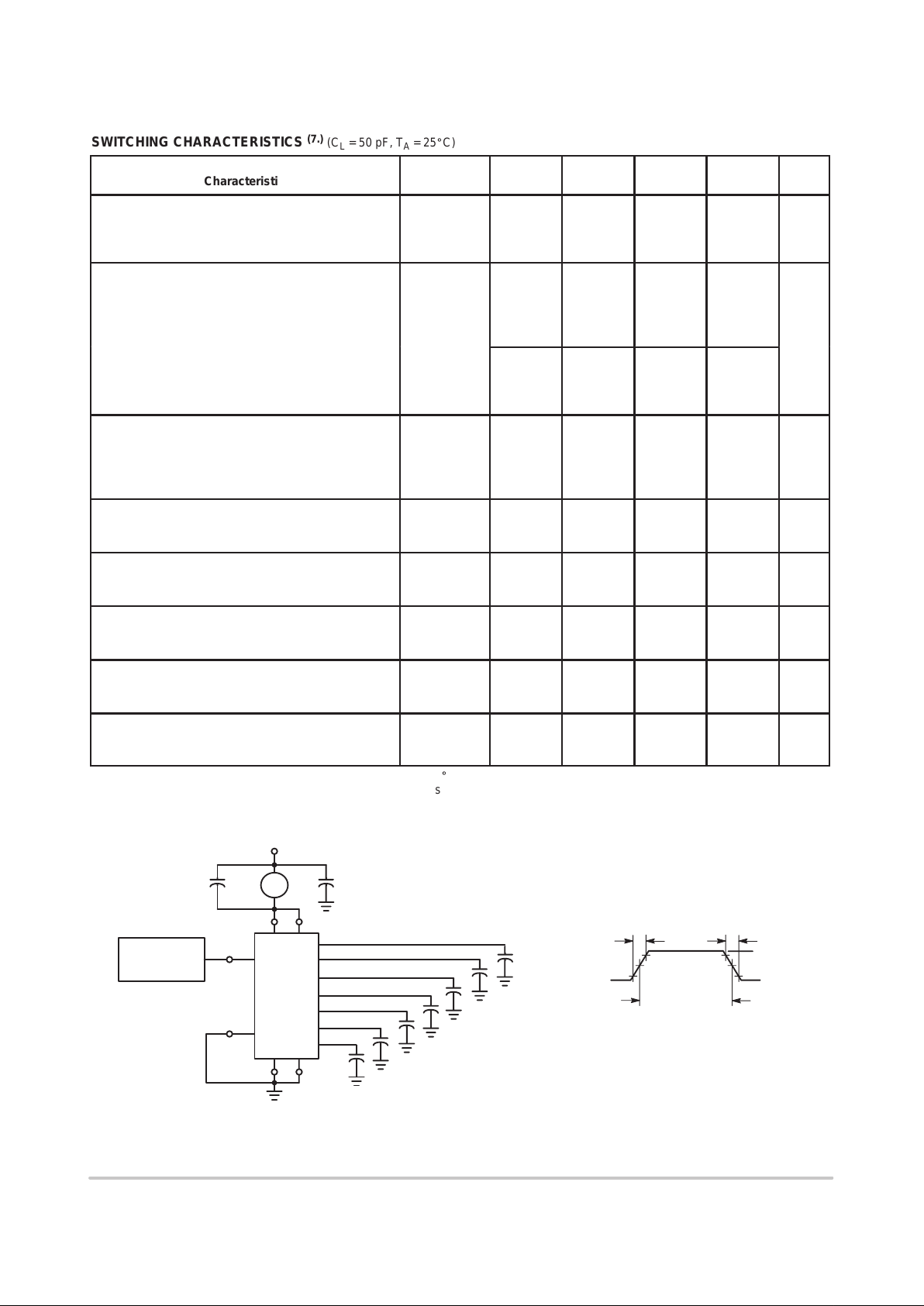
SWITCHING CHARACTERISTICS
(7.)
(C
L
= 50 pF, T
A
= 25_C)
Characteristic
Symbol
V
DD
Vdc
Min Typ
(8.)
Max Unit
Output Rise and Fall Time (Counter Outputs)
t
TLH
, t
THL
= (1.5 ns/pF) CL + 25 ns
t
TLH
, t
THL
= (0.75 ns/pF) CL + 12.5 ns
t
TLH
, t
THL
= (0.55 ns/pF) CL + 12.5 ns
t
TLH
, t
THL
5.0
10
15
—
—
—
100
50
40
200
100
80
ns
Propagation Delay Time
Clock to Q18
t
PHL
, t
PLH
= (1.7 ns/pF) CL + 4415 ns
t
PHL
, t
PLH
= (0.66 ns/pF) CL + 1667 ns
t
PHL
, t
PLH
= (0.5 ns/pF) CL + 1275 ns
t
PHL
, t
PLH
5.0
10
15
—
—
—
4.5
1.7
1.3
9.0
3.5
2.7
µs
Clock to Q24
t
PHL
, t
PLH
= (1.7 ns/pF) CL + 5915 ns
t
PHL
, t
PLH
= (0.66 ns/pF) CL + 2167 ns
t
PHL
, t
PLH
= (0.5 ns/pF) CL + 1675 ns
5.0
10
15
—
—
—
6.0
2.2
1.7
12
4.5
3.5
Propagation Delay Time
Reset to Q
n
t
PHL
= (1.7 ns/pF) CL + 1215 ns
t
PHL
= (0.66 ns/pF) CL + 467 ns
t
PHL
= (0.5 ns/pF) CL + 350 ns
t
PHL
5.0
10
15
—
—
—
1300
500
375
2600
1000
750
ns
Clock Pulse Width t
WH(cl)
5.0
10
15
385
150
120
140
55
40
—
—
—
ns
Clock Pulse Frequency f
cl
5.0
10
15
—
—
—
3.5
9.0
12
2.0
5.0
6.5
MHz
Clock Rise and Fall Time t
TLH
, t
THL
5.0
10
15
—
—
—
—
—
—
15
5.0
4.0
µs
Reset Pulse Width t
WH(R)
5.0
10
15
1400
600
450
700
300
225
—
—
—
ns
Reset Removal Time t
rem
5.0
10
15
30
0
– 40
– 200
– 160
– 110
—
—
—
ns
7. The formulas given are for the typical characteristics only at 25_C.
8. Data labelled “Typ” is not to be used for design purposes but is intended as an indication of the IC’s potential performance.
Figure 1. Power Dissipation Test Circuit and Waveform
PULSE
GENERATOR
V
DD
V
DD
V
DD
V
SS
V
SS
Q18
Q19
Q20
Q21
Q22
Q23
Q24
C
L
C
L
C
L
C
L
C
L
C
L
C
L
I
D
IN 2
R
500 µF
0.01 µF
CERAMIC
20 ns 20 ns
V
DD
0 V
V
in
50% DUTY CYCLE
90%
10%
50%
Page 5

MC14521B
http://onsemi.com
5
Figure 2. Switching Time Test Circuit and Waveforms
PULSE
GENERATOR
Q18
Q19
Q20
Q21
Q22
Q23
Q24
IN 2
R
V
DD
VDD′
V
SS
VSS′
C
L
C
L
C
L
C
L
C
L
C
L
C
L
V
DD
20 ns 20 ns 20 ns
10%
50%
90%
10%
50%
90%
IN 2
Q
n
t
PLH
t
PHL
t
TLH
t
THL
t
WL
t
WH
Characteristic
500 kHz
Circuit
50 kHz
Circuit
Unit
Crystal Characteristics
Resonant Frequency
Equivalent Resistance, R
S
500
1.0
50
6.2
kHz
kΩ
External Resistor/Capacitor Values
R
o
C
T
C
S
47
82
20
750
82
20
kΩ
pF
pF
Frequency Stability
Frequency Change as a Function
of V
DD
(TA = 25_C)
V
DD
Change from 5.0 V to 10 V
V
DD
Change from 10 V to 15 V
Frequency Change as a Function
of Temperature (VDD = 10 V)
T
A
Change from – 55_C to + 25_C
MC14521 only
Complete Oscillator*
T
A
Change from +25_C to+125_C
MC14521 only
Complete Oscillator*
+ 6.0
+ 2.0
– 4.0
+ 100
– 2.0
– 160
+ 2.0
+ 2.0
– 2.0
+ 120
– 2.0
– 560
ppm
ppm
ppm
ppm
ppm
ppm
*Complete oscillator includes crystal, capacitors, and resistors.
ООООООООООООООООО
Î
Figure 4. Typical Data for Crystal Oscillator Circuit
Figure 3. Crystal Oscillator Circuit
V
DD
VDDVDD′
V
SSVSS
′
OUT 1
OUT 2
Q18
Q19
Q20
Q21
Q22
Q23
Q24
IN 1
IN 2
R
R*
R*
C
S
C
T
R
o
18 M
*Optional for low power operation,
10 kΩ ≤ R ≤ 70 kΩ.
Page 6

MC14521B
http://onsemi.com
6
Figure 5. RC Oscillator Stability Figure 6. RC Oscillator Frequency as a
Function of RTC and C
–55 –25 0 25 50 75 100 125
8.0
4.0
0
–4.0
–8.0
–12
–16
FREQUENCY DEVIA TION (%)
TA, AMBIENT TEMPERATURE (°C), DEVICE ONLY
TEST CIRCUIT
FIGURE 7
VDD = 15 V
10 V
5.0 V
RTC = 56 kΩ,
C = 1000 pF
RS = 0, f = 10.15 kHz @ VDD = 10 V, TA = 25°C
R
S
= 120 kΩ, f = 7.8 kHz @ VDD = 10 V, TA = 25°C
{
f, OSCILLATOR FREQUENCY (kHz)
100
50
20
10
5.0
1.0
2.0
0.1
0.2
0.5
1.0 k 10 k 100 k 1.0 m
0.0001 0.001 0.01 0.1
R
TC
, RESISTANCE (OHMS)
C, CAPACITANCE (µF)
VDD = 10 V
f AS A FUNCTION
OF R
TC
(C = 1000 pF)
(R
S
≈ 2RTC)
TEST CIRCUIT
FIGURE 7
f AS A FUNCTION
OF C
(R
TC
= 56 kΩ)
(R
S
= 120 k)
Figure 7. RC Oscillator Circuit Figure 8. Functional Test Circuit
OUT 1
OUT 2
Q18
Q19
Q20
Q21
Q22
Q23
Q24
IN 1
IN 2
R
V
DDVDD
′
VSSVSS′
V
DD
R
S
R
TC
C
Q18
Q19
Q20
Q21
Q22
Q23
Q24
OUT 1
OUT 2
IN 1
IN 2
R
V
DD
′
V
DD
VSSV
SS
PULSE
GENERATOR
Page 7

MC14521B
http://onsemi.com
7
FUNCTIONAL TEST SEQUENCE
Inputs Outputs Comments
Reset In 2 Out 2 VSS′ VDD′ Q18 thru
Q24
Counter is in three 8–stage
sections in parallel mode
Counter is reset. In 2 and
1 0 0
V
DD
Gnd 0
Out 2 are connected
together
A test function (see Figure 8) has been
included for the reduction of test time re
q
uired to
0
1 1 First “0” to “1” transition
on In 2, Out 2 node.
included for the reduction of test time required to
exercise all 24 counter stages. This test function
divides the counter into three 8–stage sections,
and 255 counts are loaded in each of the
8–stage sections in parallel. All flip–flops are
now at a lo
g
ic “1”. The counter is now returned
0
1
—
—
—
0
1
—
—
—
255 “0” to “1” transitions
are clocked into this In 2,
Out 2 node.
g
to the normal 24–stages in series configuration.
One more pulse is entered into Input 2 (In 2)
1 1 1
The 255th “0” to “1”
transition.
which will cause the counter to ripple from an all
“1” state to an all “0” state.
0
0
0
0
1
1
1 0
Gnd
V
DD
1
Counter converted back to
24–stages in series mode.
1 0 1
Out 2 converts back to an
output.
0 1 0
Counter ripples from an all
“1” state to an all “0” stage.
Page 8

MC14521B
http://onsemi.com
8
LOGIC DIAGRAM
V
DD
5
RESET
2
9
IN 1
6
IN 2
7
OUT 13V
SS
4
OUT 2
STAGES
3 THRU 7
STAGES
11 THRU 15
12 8
910 16
17 18 19 20 21 22 23 24
10
Q1811Q1912Q2013Q2114Q2215Q23
1
Q24
V
DD
= PIN 16
VSS = PIN 8
Page 9

MC14521B
http://onsemi.com
9
P ACKAGE DIMENSIONS
PDIP–16
P SUFFIX
PLASTIC DIP PACKAGE
CASE 648–08
ISSUE R
NOTES:
1. DIMENSIONING AND TOLERANCING PER ANSI
Y14.5M, 1982.
2. CONTROLLING DIMENSION: INCH.
3. DIMENSION L TO CENTER OF LEADS WHEN
FORMED PARALLEL.
4. DIMENSION B DOES NOT INCLUDE MOLD FLASH.
5. ROUNDED CORNERS OPTIONAL.
–A–
B
F
C
S
H
G
D
J
L
M
16 PL
SEATING
18
916
K
PLANE
–T–
M
A
M
0.25 (0.010) T
DIM MIN MAX MIN MAX
MILLIMETERSINCHES
A 0.740 0.770 18.80 19.55
B 0.250 0.270 6.35 6.85
C 0.145 0.175 3.69 4.44
D 0.015 0.021 0.39 0.53
F 0.040 0.70 1.02 1.77
G 0.100 BSC 2.54 BSC
H 0.050 BSC 1.27 BSC
J 0.008 0.015 0.21 0.38
K 0.110 0.130 2.80 3.30
L 0.295 0.305 7.50 7.74
M 0 10 0 10
S 0.020 0.040 0.51 1.01
____
Page 10

MC14521B
http://onsemi.com
10
P ACKAGE DIMENSIONS
SOIC–16
D SUFFIX
PLASTIC SOIC PACKAGE
CASE 751B–05
ISSUE J
NOTES:
1. DIMENSIONING AND TOLERANCING PER ANSI
Y14.5M, 1982.
2. CONTROLLING DIMENSION: MILLIMETER.
3. DIMENSIONS A AND B DO NOT INCLUDE
MOLD PROTRUSION.
4. MAXIMUM MOLD PROTRUSION 0.15 (0.006)
PER SIDE.
5. DIMENSION D DOES NOT INCLUDE DAMBAR
PROTRUSION. ALLOWABLE DAMBAR
PROTRUSION SHALL BE 0.127 (0.005) TOTAL
IN EXCESS OF THE D DIMENSION AT
MAXIMUM MATERIAL CONDITION.
18
16 9
SEATING
PLANE
F
J
M
R
X 45
_
G
8 PLP
–B–
–A–
M
0.25 (0.010) B
S
–T–
D
K
C
16 PL
S
B
M
0.25 (0.010) A
S
T
DIM MIN MAX MIN MAX
INCHESMILLIMETERS
A 9.80 10.00 0.386 0.393
B 3.80 4.00 0.150 0.157
C 1.35 1.75 0.054 0.068
D 0.35 0.49 0.014 0.019
F 0.40 1.25 0.016 0.049
G 1.27 BSC 0.050 BSC
J 0.19 0.25 0.008 0.009
K 0.10 0.25 0.004 0.009
M 0 7 0 7
P 5.80 6.20 0.229 0.244
R 0.25 0.50 0.010 0.019
____
Page 11

MC14521B
http://onsemi.com
11
P ACKAGE DIMENSIONS
H
E
A
1
DIM MIN MAX MIN MAX
INCHES
––– 2.05 ––– 0.081
MILLIMETERS
0.05 0.20 0.002 0.008
0.35 0.50 0.014 0.020
0.18 0.27 0.007 0.011
9.90 10.50 0.390 0.413
5.10 5.45 0.201 0.215
1.27 BSC 0.050 BSC
7.40 8.20 0.291 0.323
0.50 0.85 0.020 0.033
1.10 1.50 0.043 0.059
0
0.70 0.90 0.028 0.035
––– 0.78 ––– 0.031
A
1
H
E
Q
1
L
E
_
10
_
0
_
10
_
L
E
Q
1
_
NOTES:
1. DIMENSIONING AND TOLERANCING PER ANSI
Y14.5M, 1982.
2. CONTROLLING DIMENSION: MILLIMETER.
3. DIMENSIONS D AND E DO NOT INCLUDE
MOLD FLASH OR PROTRUSIONS AND ARE
MEASURED AT THE PARTING LINE. MOLD FLASH
OR PROTRUSIONS SHALL NOT EXCEED 0.15
(0.006) PER SIDE.
4. TERMINAL NUMBERS ARE SHOWN FOR
REFERENCE ONLY.
5. THE LEAD WIDTH DIMENSION (b) DOES NOT
INCLUDE DAMBAR PROTRUSION. ALLOWABLE
DAMBAR PROTRUSION SHALL BE 0.08 (0.003)
TOTAL IN EXCESS OF THE LEAD WIDTH
DIMENSION AT MAXIMUM MATERIAL CONDITION.
DAMBAR CANNOT BE LOCATED ON THE LOWER
RADIUS OR THE FOOT. MINIMUM SPACE
BETWEEN PROTRUSIONS AND ADJACENT LEAD
TO BE 0.46 ( 0.018).
M
L
DETAIL P
VIEW P
c
A
b
e
M
0.13 (0.005)
0.10 (0.004)
1
16 9
8
D
Z
E
A
b
c
D
E
e
L
M
Z
SOEIAJ–16
F SUFFIX
PLASTIC EIAJ SOIC PACKAGE
CASE 966–01
ISSUE O
Page 12

MC14521B
http://onsemi.com
12
ON Semiconductor and are trademarks of Semiconductor Components Industries, LLC (SCILLC). SCILLC reserves the right to make changes
without further notice to any products herein. SCILLC makes no warranty , representation or guarantee regarding the suitability of its products for any particular
purpose, nor does SCILLC assume any liability arising out of the application or use of any product or circuit, and specifically disclaims any and all liability ,
including without limitation special, consequential or incidental damages. “Typical” parameters which may be provided in SCILLC data sheets and/or
specifications can and do vary in different applications and actual performance may vary over time. All operating parameters, including “Typicals” must be
validated for each customer application by customer’s technical experts. SCILLC does not convey any license under its patent rights nor the rights of others.
SCILLC products are not designed, intended, or authorized for use as components in systems intended for surgical implant into the body, or other applications
intended to support or sustain life, or for any other application in which the failure of the SCILLC product could create a situation where personal injury or
death may occur. Should Buyer purchase or use SCILLC products for any such unintended or unauthorized application, Buyer shall indemnify and hold
SCILLC and its officers, employees, subsidiaries, affiliates, and distributors harmless against all claims, costs, damages, and expenses, and reasonable
attorney fees arising out of, directly or indirectly , any claim of personal injury or death associated with such unintended or unauthorized use, even if such claim
alleges that SCILLC was negligent regarding the design or manufacture of the part. SCILLC is an Equal Opportunity/Affirmative Action Employer .
PUBLICATION ORDERING INFORMATION
CENTRAL/SOUTH AMERICA:
Spanish Phone: 303–308–7143 (Mon–Fri 8:00am to 5:00pm MST)
Email: ONlit–spanish@hibbertco.com
ASIA/PACIFIC : LDC for ON Semiconductor – Asia Support
Phone: 303–675–2121 (T ue–Fri 9:00am to 1:00pm, Hong Kong Time)
T oll Free from Hong Kong & Singapore:
001–800–4422–3781
Email: ONlit–asia@hibbertco.com
JAPAN: ON Semiconductor, Japan Customer Focus Center
4–32–1 Nishi–Gotanda, Shinagawa–ku, T okyo, Japan 141–8549
Phone: 81–3–5740–2745
Email: r14525@onsemi.com
ON Semiconductor Website: http://onsemi.com
For additional information, please contact your local
Sales Representative.
MC14521B/D
NORTH AMERICA Literature Fulfillment:
Literature Distribution Center for ON Semiconductor
P.O. Box 5163, Denver, Colorado 80217 USA
Phone: 303–675–2175 or 800–344–3860 T oll Free USA/Canada
Fax: 303–675–2176 or 800–344–3867 Toll Free USA/Canada
Email: ONlit@hibbertco.com
Fax Response Line: 303–675–2167 or 800–344–3810 T oll Free USA/Canada
N. American Technical Support: 800–282–9855 Toll Free USA/Canada
EUROPE: LDC for ON Semiconductor – European Support
German Phone: (+1) 303–308–7140 (M–F 1:00pm to 5:00pm Munich Time)
Email: ONlit–german@hibbertco.com
French Phone: (+1) 303–308–7141 (M–F 1:00pm to 5:00pm Toulouse T ime)
Email: ONlit–french@hibbertco.com
English Phone: (+1) 303–308–7142 (M–F 12:00pm to 5:00pm UK Time)
Email: ONlit@hibbertco.com
EUROPEAN TOLL–FREE ACCESS*: 00–800–4422–3781
*Available from Germany, France, Italy , England, Ireland
 Loading...