

Page 1
MOTOROLA CMOS LOGIC DATA
1
MC14521B
" !
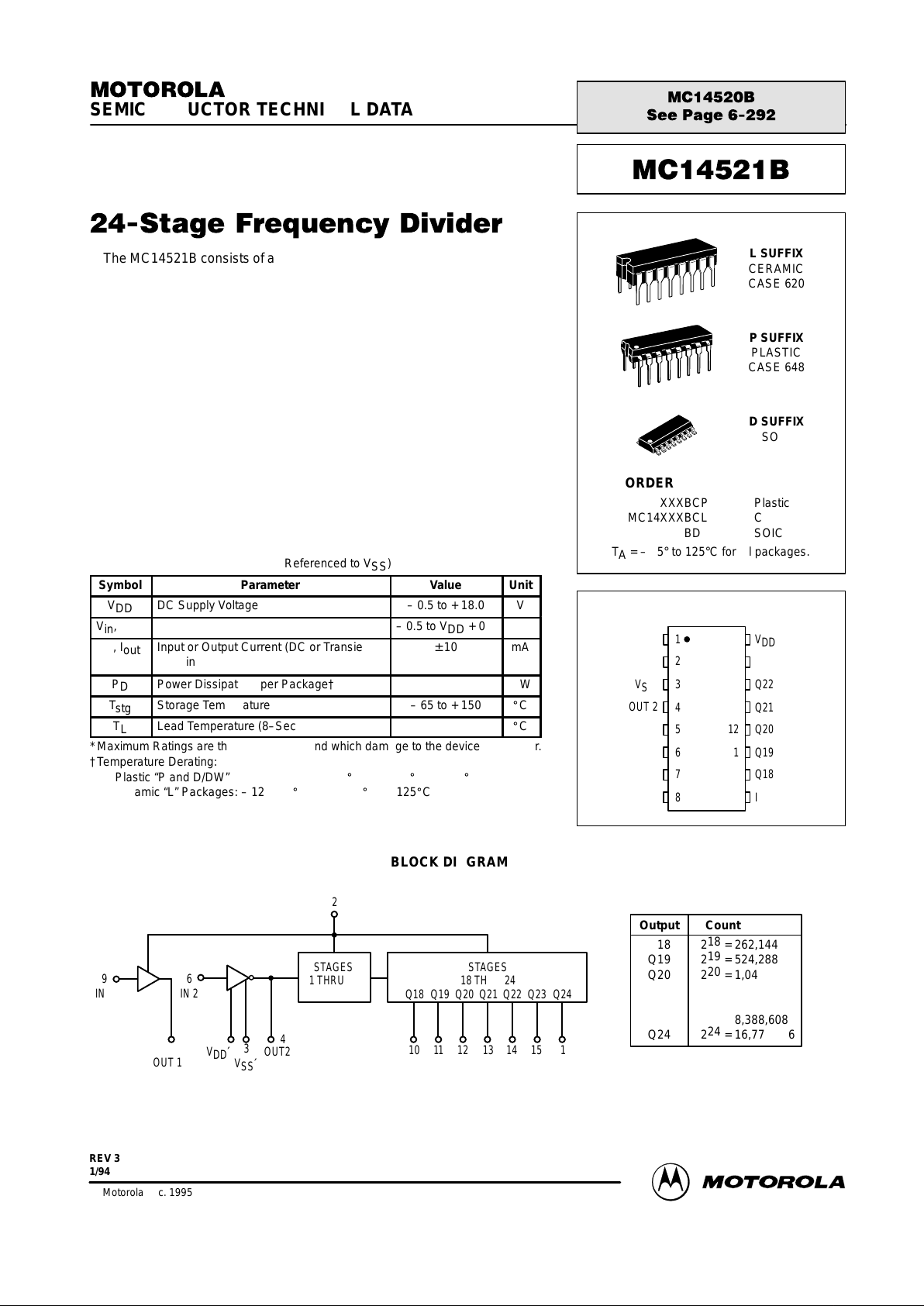
The MC14521B consists of a chain of 24 flip–flops with an input circuit that
allows three modes of operation. The i nput will function as a crystal
oscillator, an RC oscillator, or as an input buffer for an external oscillator.
Each flip–flop divides the frequency of t he previous flip–flop by two,
consequently this part will count up to 224 = 16,777,216. The count advances
on the n egative g oing e dge o f the c lock. T he outputs o f the l ast
seven–stages are available for added flexibility.
• All Stages are Resettable
• Reset Disables the RC Oscillator for Low Standby Power Drain
• RC and Crystal Oscillator Outputs Are Capable of Driving External
Loads
• Test Mode to Reduce Test Time
• VDD′ and VSS′ Pins Brought Out on Crystal Oscillator Inverter to Allow
the Connection of External Resistors for Low–Power Operation
• Supply Voltage Range = 3.0 Vdc to 18 Vdc
• Capable of Driving Two Low–power TTL Loads or One Low–power
Schottky TTL Load over the Rated Temperature Range.
MAXIMUM RATINGS* (Voltages Referenced to V
SS
)
Symbol
Parameter
Value
Unit
V
DD
DC Supply Voltage
– 0.5 to + 18.0
V
Vin, V
out
Input or Output Voltage (DC or Transient)
– 0.5 to VDD + 0.5
V
Iin, I
out
Input or Output Current (DC or Transient),
per Pin
± 10
mA
P
D
Power Dissipation, per Package†
500
mW
T
stg
Storage Temperature
– 65 to + 150
_
C
T
L
Lead Temperature (8–Second Soldering)
260
_
C
*Maximum Ratings are those values beyond which damage to the device may occur.
†Temperature Derating:
Plastic “P and D/DW” Packages: – 7.0 mW/_C From 65_C To 125_C
Ceramic “L” Packages: – 12 mW/_C From 100_C To 125_C
BLOCK DIAGRAM
Output Count Capacity
Q18 218 = 262,144
Q19 219 = 524,288
Q20 220 = 1,048,576
Q21 221 = 2,097,152
Q22 222 = 4,194,304
Q23 223 = 8,388,608
Q24 224 = 16,777,216
STAGES
18 THRU 24
STAGES
1 THRU 17
Q18 Q19 Q20 Q21 Q22 Q23 Q24
10 11 12 13 14 15 1
2
6
IN 2
9
IN 1
7
RESET
VDD = PIN 16
VSS = PIN 8
5
3
4
OUT 1
V
DD
′
VSS′
OUT2
SEMICONDUCTOR TECHNICAL DATA
Motorola, Inc. 1995
REV 3
1/94
L SUFFIX
CERAMIC
CASE 620
ORDERING INFORMATION
MC14XXXBCP Plastic
MC14XXXBCL Ceramic
MC14XXXBD SOIC
TA = – 55° to 125°C for all packages.
P SUFFIX
PLASTIC
CASE 648
D SUFFIX
SOIC
CASE 751B
PIN ASSIGNMENT
13
14
15
16
9
10
11
125
4
3
2
1
8
7
6
Q20
Q21
Q22
V
DD
IN 1
Q18
Q19
OUT 2
V
SS
′
RESET
Q24
V
SS
OUT 1
IN 2
V
DD
′
Q23
Page 2
MOTOROLA CMOS LOGIC DATAMC14521B
2
ELECTRICAL CHARACTERISTICS (Voltages Referenced to V
SS
)
V
– 55_C 25_C 125_C
Characteristic
Symbol
V
DD
Vdc
Min Max Min Typ # Max Min Max
Unit
Output Voltage
“0” Level
Vin = VDD or 0
V
OL
5.0
10
15
—
—
—
0.05
0.05
0.05
—
—
—
0
0
0
0.05
0.05
0.05
—
—
—
0.05
0.05
0.05
Vdc
“1” Level
Vin = 0 or V
DD
V
OH
5.0
10
15
4.95
9.95
14.95
—
—
—
4.95
9.95
14.95
5.0
10
15
—
—
—
4.95
9.95
14.95
—
—
—
Vdc
Input Voltage
“0” Level
(VO = 4.5 or 0.5 Vdc)
(VO = 9.0 or 1.0 Vdc)
(VO = 13.5 or 1.5 Vdc)
V
IL
5.0
10
15
—
—
—
1.5
3.0
4.0
—
—
—
2.25
4.50
6.75
1.5
3.0
4.0
—
—
—
1.5
3.0
4.0
Vdc
“1” Level
(VO = 0.5 or 4.5 Vdc)
(VO = 1.0 or 9.0 Vdc)
(VO = 1.5 or 13.5 Vdc)
V
IH
5.0
10
15
3.5
7.0
11
—
—
—
3.5
7.0
11
2.75
5.50
8.25
—
—
—
3.5
7.0
11
—
—
—
Vdc
Output Drive Current
(VOH = 2.5 Vdc) Source
(VOH = 4.6 Vdc) Pins 4 & 7
(VOH = 9.5 Vdc)
(VOH = 13.5 Vdc)
I
OH
5.0
5.0
10
15
– 1.2
– 0.25
– 0.62
– 1.8
—
—
—
—
– 1.0
– 0.2
– 0.5
– 1.5
– 1.7
– 0.36
– 0.9
– 3.5
—
—
—
—
– 0.7
– 0.14
– 0.35
– 1.1
—
—
—
—
mAdc
(VOH = 2.5 Vdc) Source
(VOH = 4.6 Vdc)
Pins 1, 10,
(VOH = 9.5 Vdc) 11, 12, 13, 14
(VOH = 13.5 Vdc) and 15
5.0
5.0
10
15
– 3.0
– 0.64
– 1.6
– 4.2
—
—
—
—
– 2.4
– 0.51
– 1.3
– 3.4
– 4.2
– 0.88
– 2.25
– 8.8
—
—
—
—
– 1.7
– 0.36
– 0.9
– 2.4
—
—
—
—
mAdc
(VOL = 0.4 Vdc) Sink
(VOL = 0.5 Vdc)
(VOL = 1.5 Vdc)
I
OL
5.0
10
15
0.64
1.6
4.2
—
—
—
0.51
1.3
3.4
0.88
2.25
8.8
—
—
—
0.36
0.9
2.4
—
—
—
mAdc
Input Current I
in
15 — ± 0.1 — ±0.00001 ± 0.1 — ± 1.0 µAdc
Input Capacitance
(Vin = 0)
C
in
— — — — 5.0 7.5 — — pF
Quiescent Current
(Per Package)
I
DD
5.0
10
15
—
—
—
5.0
10
20
—
—
—
0.005
0.010
0.015
5.0
10
20
—
—
—
150
300
600
µAdc
Total Supply Current**†
(Dynamic plus Quiescent,
Per Package)
(CL = 50 pF on all outputs, all
buffers switching)
I
T
5.0
10
15
IT = (0.42 µA/kHz) f + I
DD
IT = (0.85 µA/kHz) f + I
DD
IT = (1.40 µA/kHz) f + I
DD
µAdc
#Data labelled “Typ” is not to be used for design purposes but is intended as an indication of the IC’s potential performance.
**The formulas given are for the typical characteristics only at 25_C.
†To calculate total supply current at loads other than 50 pF:
IT(CL) = IT(50 pF) + (CL – 50) Vfk
where: IT is in µA (per package), CL in pF, V = (VDD – VSS) in volts, f in kHz is input frequency, and k = 0.003.
This device contains protection circuitry to guard against damage due to high static voltages or electric fields. However,
precautions must be taken to avoid applications of any voltage higher than maximum rated voltages to this high-impedance
circuit. For proper operation, Vin and V
out
should be constrained to the range VSS ≤ (Vin or V
out
) ≤ VDD.
Unused inputs must always be tied to an appropriate logic voltage level (e.g., either VSS or VDD). Unused outputs must
be left open.
Page 3
MOTOROLA CMOS LOGIC DATA
3
MC14521B
SWITCHING CHARACTERISTICS* (C
L
= 50 pF, TA = 25_C)
Characteristic
Symbol
V
DD
Vdc
Min Typ # Max Unit
Output Rise and Fall Time (Counter Outputs)
t
TLH
, t
THL
= (1.5 ns/pF) CL + 25 ns
t
TLH
, t
THL
= (0.75 ns/pF) CL + 12.5 ns
t
TLH
, t
THL
= (0.55 ns/pF) CL + 12.5 ns
t
TLH
, t
THL
5.0
10
15
—
—
—
100
50
40
200
100
80
ns
Propagation Delay Time
Clock to Q18
t
PHL
, t
PLH
= (1.7 ns/pF) CL + 4415 ns
t
PHL
, t
PLH
= (0.66 ns/pF) CL + 1667 ns
t
PHL
, t
PLH
= (0.5 ns/pF) CL + 1275 ns
t
PHL
, t
PLH
5.0
10
15
—
—
—
4.5
1.7
1.3
9.0
3.5
2.7
µs
Clock to Q24
t
PHL
, t
PLH
= (1.7 ns/pF) CL + 5915 ns
t
PHL
, t
PLH
= (0.66 ns/pF) CL + 2167 ns
t
PHL
, t
PLH
= (0.5 ns/pF) CL + 1675 ns
5.0
10
15
—
—
—
6.0
2.2
1.7
12
4.5
3.5
Propagation Delay Time
Reset to Q
n
t
PHL
= (1.7 ns/pF) CL + 1215 ns
t
PHL
= (0.66 ns/pF) CL + 467 ns
t
PHL
= (0.5 ns/pF) CL + 350 ns
t
PHL
5.0
10
15
—
—
—
1300
500
375
2600
1000
750
ns
Clock Pulse Width t
WH(cl)
5.0
10
15
385
150
120
140
55
40
—
—
—
ns
Clock Pulse Frequency f
cl
5.0
10
15
—
—
—
3.5
9.0
12
2.0
5.0
6.5
MHz
Clock Rise and Fall Time t
TLH
, t
THL
5.0
10
15
—
—
—
—
—
—
15
5.0
4.0
µs
Reset Pulse Width t
WH(R)
5.0
10
15
1400
600
450
700
300
225
—
—
—
ns
Reset Removal Time t
rem
5.0
10
15
30
0
– 40
– 200
– 160
– 110
—
—
—
ns
*The formulas given are for the typical characteristics only at 25_C.
#Data labelled “Typ” is not to be used for design purposes but is intended as an indication of the IC’s potential performance.
Figure 1. Power Dissipation Test Circuit and Waveform
PULSE
GENERATOR
V
DD
V
DD
V
DD
V
SS
V
SS
Q18
Q19
Q20
Q21
Q22
Q23
Q24
C
L
C
L
C
L
C
L
C
L
C
L
C
L
I
D
IN 2
R
500
µ
F
0.01 µF
CERAMIC
20 ns 20 ns
V
DD
0 V
V
in
50% DUTY CYCLE
90%
10%
50%
Page 4

MOTOROLA CMOS LOGIC DATAMC14521B
4
Figure 2. Switching Time Test Circuit and Waveforms
PULSE
GENERATOR
Q18
Q19
Q20
Q21
Q22
Q23
Q24
IN 2
R
V
DD
V
DD
′
V
SS
VSS′
C
L
C
L
C
L
C
L
C
L
C
L
C
L
V
DD
20 ns 20 ns 20 ns
10%
50%
90%
10%
50%
90%
IN 2
Q
n
t
PLH
t
PHL
t
TLH
t
THL
t
WL
t
WH
Characteristic
500 kHz
Circuit
50 kHz
Circuit
Unit
Crystal Characteristics
Resonant Frequency
Equivalent Resistance, R
S
500
1.0
50
6.2
kHz
kΩ
External Resistor/Capacitor Values
R
o
C
T
C
S
47
82
20
750
82
20
kΩ
pF
pF
Frequency Stability
Frequency Change as a Function
of VDD (TA = 25_C)
VDD Change from 5.0 V to 10 V
VDD Change from 10 V to 15 V
Frequency Change as a Function
of Temperature (VDD = 10 V)
TA Change from – 55_C to + 25_C
MC14521 only
Complete Oscillator*
TA Change from +25_C to+125_C
MC14521 only
Complete Oscillator*
+ 6.0
+ 2.0
– 4.0
+ 100
– 2.0
– 160
+ 2.0
+ 2.0
– 2.0
+ 120
– 2.0
– 560
ppm
ppm
ppm
ppm
ppm
ppm
*Complete oscillator includes crystal, capacitors, and resistors.
Figure 4. Typical Data for Crystal Oscillator Circuit
Figure 3. Crystal Oscillator Circuit
V
DD
VDDV
DD
′
VSSVSS′
OUT 1
OUT 2
Q18
Q19
Q20
Q21
Q22
Q23
Q24
IN 1
IN 2
R
R*
R*
C
S
C
T
R
o
18 M
*Optional for low power operation,
10 kΩ ≤ R ≤ 70 kΩ.
Page 5

MOTOROLA CMOS LOGIC DATA
5
MC14521B
Figure 5. RC Oscillator Stability Figure 6. RC Oscillator Frequency as a
Function of RTC and C
–55 –25 0 25 50 75 100 125
8.0
4.0
0
–4.0
–8.0
–12
–16
FREQUENCY DEVIATION (%)
TA, AMBIENT TEMPERATURE (°C), DEVICE ONLY
TEST CIRCUIT
FIGURE 7
VDD = 15 V
10 V
5.0 V
RTC = 56 kΩ,
C = 1000 pF
RS = 0, f = 10.15 kHz @ VDD = 10 V, TA = 25°C
RS = 120 k
Ω
, f = 7.8 kHz @ VDD = 10 V, TA = 25°C
{
f, OSCILLATOR FREQUENCY (kHz)
100
50
20
10
5.0
1.0
2.0
0.1
0.2
0.5
1.0 k 10 k 100 k 1.0 m
0.0001 0.001 0.01 0.1
RTC, RESISTANCE (OHMS)
C, CAPACITANCE (
µ
F)
VDD = 10 V
f AS A FUNCTION
OF R
TC
(C = 1000 pF)
(RS ≈ 2RTC)
TEST CIRCUIT
FIGURE 7
f AS A FUNCTION
OF C
(RTC = 56 kΩ)
(RS = 120 k)
Figure 7. RC Oscillator Circuit Figure 8. Functional Test Circuit
OUT 1
OUT 2
Q18
Q19
Q20
Q21
Q22
Q23
Q24
IN 1
IN 2
R
VDDV
DD
′
VSSVSS′
V
DD
R
S
R
TC
C
Q18
Q19
Q20
Q21
Q22
Q23
Q24
OUT 1
OUT 2
IN 1
IN 2
R
V
DD
′
V
DD
VSSV
SS
PULSE
GENERATOR
FUNCTIONAL TEST SEQUENCE
Inputs Outputs Comments
Reset In 2 Out 2 VSS′ VDD′ Q18 thru Q24
Counter is in three 8–stage
sections in parallel mode
1 0 0
V
DD
Gnd 0
Counter is reset. In 2 and
Out 2 are connected
together
A test function (see Figure 8) has been
included for the reduction of test time required to
0
1 1 First “0” to “1” transition
on In 2, Out 2 node.
included for the reduction of test time required to
exercise all 24 counter stages. This test function
divides the counter into three 8–stage sections,
and 255 counts are loaded in each of the
8–stage sections in parallel. All flip–flops are
now at a logic “1”. The counter is now returned
0
1
—
—
—
0
1
—
—
—
255 “0” to “1” transitions
are clocked into this In 2,
Out 2 node.
now at a logic “1”. The counter is now returned
to the normal 24–stages in series configuration.
One more pulse is entered into Input 2 (In 2)
1 1 1
The 255th “0” to “1”
transition.
which
will cause the counter to ripple from an all
“1” state to an all “0” state.
0
0
0
0
Gnd
1
1
1 0
Gnd
V
DD
1
Counter converted back to
24–stages in series mode.
1 0 1
Out 2 converts back to an
output.
0 1 0
Counter ripples from an all
“1” state to an all “0” stage.
Page 6

MOTOROLA CMOS LOGIC DATAMC14521B
6
LOGIC DIAGRAM
V
DD
5
RESET
2
9
IN 1
6
IN 2
7
OUT 13V
SS
4
OUT 2
STAGES
3 THRU 7
STAGES
11 THRU 15
1 2 8
9 10 16
17 18 19 20 21 22 23 24
10
Q1811Q1912Q2013Q2114Q2215Q23
1
Q24
VDD = PIN 16
VSS = PIN 8
Page 7

MOTOROLA CMOS LOGIC DATA
7
MC14521B
OUTLINE DIMENSIONS
P SUFFIX
PLASTIC DIP PACKAGE
CASE 648–08
ISSUE R
NOTES:
1. DIMENSIONING AND TOLERANCING PER ANSI
Y14.5M, 1982.
2. CONTROLLING DIMENSION: INCH.
3. DIMENSION L TO CENTER OF LEADS WHEN
FORMED PARALLEL.
4. DIMENSION B DOES NOT INCLUDE MOLD FLASH.
5. ROUNDED CORNERS OPTIONAL.
–A–
B
F
C
S
H
G
D
J
L
M
16 PL
SEATING
1 8
916
K
PLANE
–T–
M
A
M
0.25 (0.010) T
DIM MIN MAX MIN MAX
MILLIMETERSINCHES
A 0.740 0.770 18.80 19.55
B 0.250 0.270 6.35 6.85
C 0.145 0.175 3.69 4.44
D 0.015 0.021 0.39 0.53
F 0.040 0.70 1.02 1.77
G 0.100 BSC 2.54 BSC
H 0.050 BSC 1.27 BSC
J 0.008 0.015 0.21 0.38
K 0.110 0.130 2.80 3.30
L 0.295 0.305 7.50 7.74
M 0 10 0 10
S 0.020 0.040 0.51 1.01
____
L SUFFIX
CERAMIC DIP PACKAGE
CASE 620–10
ISSUE V
NOTES:
1. DIMENSIONING AND TOLERANCING PER
ANSI Y14.5M, 1982.
2. CONTROLLING DIMENSION: INCH.
3. DIMENSION L TO CENTER OF LEAD WHEN
FORMED PARALLEL.
4. DIMENSION F MAY NARROW TO 0.76 (0.030)
WHERE THE LEAD ENTERS THE CERAMIC
BODY.
–A–
–B–
–T–
F
E
G
N
K
C
SEATING
PLANE
16 PLD
S
A
M
0.25 (0.010) T
16 PLJ
S
B
M
0.25 (0.010) T
M
L
DIM MIN MAX MIN MAX
MILLIMETERSINCHES
A 0.750 0.785 19.05 19.93
B 0.240 0.295 6.10 7.49
C ––– 0.200 ––– 5.08
D 0.015 0.020 0.39 0.50
E 0.050 BSC 1.27 BSC
F 0.055 0.065 1.40 1.65
G 0.100 BSC 2.54 BSC
H 0.008 0.015 0.21 0.38
K 0.125 0.170 3.18 4.31
L 0.300 BSC 7.62 BSC
M 0 15 0 15
N 0.020 0.040 0.51 1.01
_ _ _ _
16 9
1 8
Page 8

MOTOROLA CMOS LOGIC DATAMC14521B
8
OUTLINE DIMENSIONS
D SUFFIX
PLASTIC SOIC PACKAGE
CASE 751B–05
ISSUE J
NOTES:
1. DIMENSIONING AND TOLERANCING PER ANSI
Y14.5M, 1982.
2. CONTROLLING DIMENSION: MILLIMETER.
3. DIMENSIONS A AND B DO NOT INCLUDE
MOLD PROTRUSION.
4. MAXIMUM MOLD PROTRUSION 0.15 (0.006)
PER SIDE.
5. DIMENSION D DOES NOT INCLUDE DAMBAR
PROTRUSION. ALLOWABLE DAMBAR
PROTRUSION SHALL BE 0.127 (0.005) TOTAL
IN EXCESS OF THE D DIMENSION AT
MAXIMUM MATERIAL CONDITION.
1 8
16 9
SEATING
PLANE
F
J
M
R
X 45
_
G
8 PLP
–B–
–A–
M
0.25 (0.010) B
S
–T–
D
K
C
16 PL
S
B
M
0.25 (0.010) A
S
T
DIM MIN MAX MIN MAX
INCHESMILLIMETERS
A 9.80 10.00 0.386 0.393
B 3.80 4.00 0.150 0.157
C 1.35 1.75 0.054 0.068
D 0.35 0.49 0.014 0.019
F 0.40 1.25 0.016 0.049
G 1.27 BSC 0.050 BSC
J 0.19 0.25 0.008 0.009
K 0.10 0.25 0.004 0.009
M 0 7 0 7
P 5.80 6.20 0.229 0.244
R 0.25 0.50 0.010 0.019
_ _ _ _
How to reach us:
USA/EUROPE/Locations Not Listed: Motorola Literature Distribution; JAPAN: Nippon Motorola Ltd.; Tatsumi–SPD–JLDC, 6F Seibu–Butsuryu–Center,
P.O. Box 20912; Phoenix, Arizona 85036. 1–800–441–2447 or 602–303–5454 3–14–2 Tatsumi Koto–Ku, Tokyo 135, Japan. 03–81–3521–8315
MFAX: RMFAX0@email.sps.mot.com – TOUCHTONE 602–244–6609 ASIA/PACIFIC: Motorola Semiconductors H.K. Ltd.; 8B Tai Ping Industrial Park,
INTERNET: http://Design–NET.com 51 Ting Kok Road, Tai Po, N.T., Hong Kong. 852–26629298
Motorola reserves the right to make changes without further notice to any products herein. Motorola makes no warranty , representation or guarantee regarding
the suitability of its products for any particular purpose, nor does Motorola assume any liability arising out of the application or use of any product or circuit,
and specifically disclaims any and all liability, including without limitation consequential or incidental damages. “Typical” parameters which may be provided
in Motorola data sheets and/or specifications can and do vary in different applications and actual performance may vary over time. All operating parameters,
including “Typicals” must be validated for each customer application by customer’s technical experts. Motorola does not convey any license under its patent
rights nor the rights of others. Motorola products are not designed, intended, or authorized for use as components in systems intended for surgical implant
into the body, or other applications intended to support or sustain life, or for any other application in which the failure of the Motorola product could create a
situation where personal injury or death may occur. Should Buyer purchase or use Motorola products for any such unintended or unauthorized application,
Buyer shall indemnify and hold Motorola and its officers, employees, subsidiaries, affiliates, and distributors harmless against all claims, costs, damages, and
expenses, and reasonable attorney fees arising out of, directly or indirectly, any claim of personal injury or death associated with such unintended or
unauthorized use, even if such claim alleges that Motorola was negligent regarding the design or manufacture of the part. Motorola and are registered
trademarks of Motorola, Inc. Motorola, Inc. is an Equal Opportunity/Affirmative Action Employer .
MC14521B/D
*MC14521B/D*
◊
 Loading...