

Page 1
MC14517B
Dual 64-Bit Static Shift
Register
The MC14517B dual 64–bit static shift register consists of two
identical, independent, 64–bit registers. Each register has separate clock
and write enable inputs, as well as outputs at bits 16, 32, 48, and 64. Data
at the data input is entered by clocking, regardless of the state of the write
enable input. An output is disabled (open circuited) when the write enable
input is high. During this time, data appearing at the data input as well as
the 16–bit, 32–bit, and 48–bit taps may be entered into the device by
application of a clock pulse. This feature permits the register to be loaded
with 64 bits in 16 clock periods, and also permits bus logic to be used.
This device is useful in time delay circuits, temporary memory storage
circuits, and other serial shift register applications.
• Diode Protection on All Inputs
• Fully Static Operation
• Output Transitions Occur on the Rising Edge of the Clock Pulse
• Exceedingly Slow Input Transition Rates May Be Applied to the
Clock Input
• 3–State Output at 64th–Bit Allows Use in Bus Logic Applications
• Shift Registers of any Length may be Fully Loaded with 16 Clock
Pulses
• Supply Voltage Range = 3.0 Vdc to 18 Vdc
• Capable of Driving T wo Low–power TTL Loads or One Low–power
Schottky TTL Load Over the Rated T emperature Range
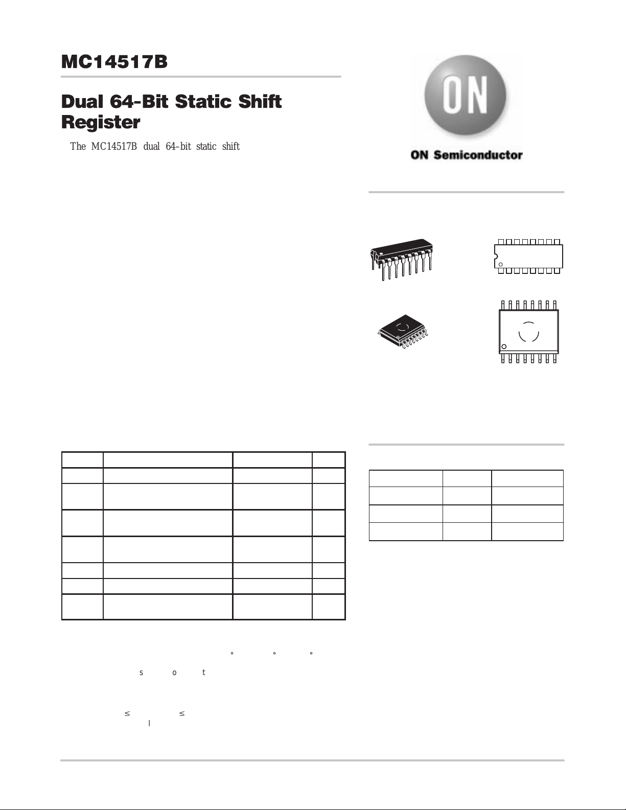
http://onsemi.com
MARKING
DIAGRAMS
16
PDIP–16
P SUFFIX
CASE 648
SOIC–16
DW SUFFIX
CASE 751G
A = Assembly Location
WL or L = Wafer Lot
YY or Y = Year
WW or W = Work Week
MC14517BCP
AWLYYWW
1
16
AWLYYWW
1
14517B
MAXIMUM RATINGS (Voltages Referenced to V
Symbol
V
DD
Vin, V
Iin, I
P
T
T
stg
T
1. Maximum Ratings are those values beyond which damage to the device
may occur.
2. Temperature Derating:
Plastic “P and D/DW” Packages: – 7.0 mW/_C From 65_C To 125_C
This device contains protection circuitry to guard against damage due to high
static voltages or electric fields. However, precautions must be taken to avoid
applications of any voltage higher than maximum rated voltages to this
high–impedance circuit. For proper operation, V
to the range V
Unused inputs must always be tied to an appropriate logic voltage level (e.g.,
either V
DC Supply Voltage Range –0.5 to +18.0 V
Input or Output Voltage Range
out
Input or Output Current
out
Power Dissipation,
D
Operating Temperature Range –55 to +125 °C
A
Storage Temperature Range –65 to +150 °C
Lead Temperature
L
SS
or VDD). Unused outputs must be left open.
SS
Parameter Value Unit
(DC or Transient)
(DC or Transient) per Pin
per Package (Note 2.)
(8–Second Soldering)
v (Vin or V
) v VDD.
out
) (Note 1.)
SS
–0.5 to VDD + 0.5 V
±10 mA
500 mW
260 °C
and V
in
should be constrained
out
ORDERING INFORMATION
Device Package Shipping
MC14517BCP PDIP–16 2000/Box
MC14517BDW SOIC–16 47/Rail
MC14517BDWR2 SOIC–16 1000/Tape & Reel
Semiconductor Components Industries, LLC, 2000
March, 2000 – Rev . 3
1 Publication Order Number:
MC14517B/D
Page 2
MC14517B
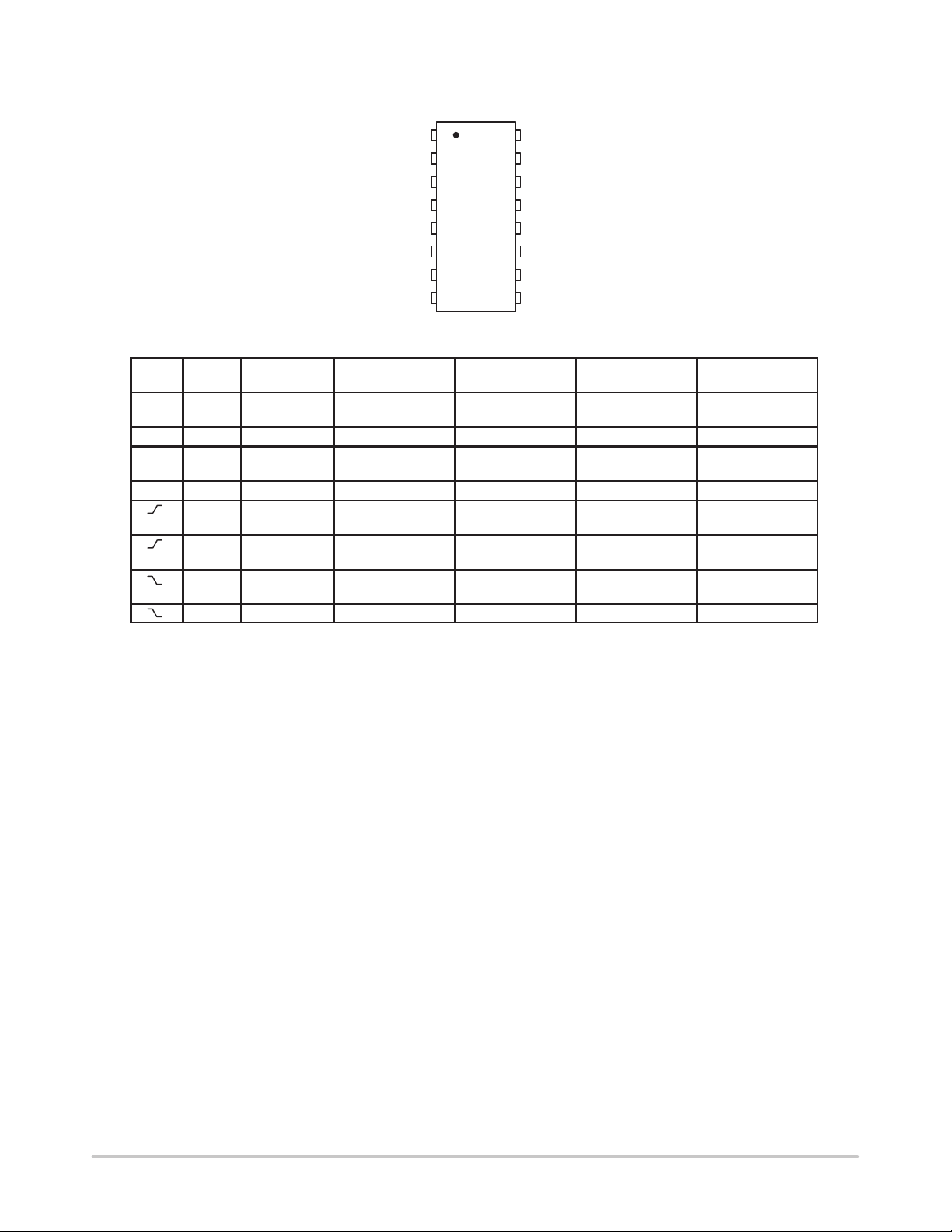
PIN ASSIGNMENT
Q16
Q48
WE
Q64
Q32
V
1
A
2
A
3
A
C
4
A
A
6
A
D
7
A
8
SS
16
V
DD
15
Q16
B
Q48
14
13
125
11
10
B
WE
B
C
B
Q64
B
Q32
B
D
9
B
FUNCTIONAL TRUTH TABLE (X = Don’t Care)
Write
Clock
Enable
0 0 X Content of 16–Bit
Data 16–Bit Tap 32–Bit Tap 48–Bit Tap 64–Bit Tap
Displayed
Content of 32–Bit
Displayed
Content of 48–Bit
Displayed
Content of 64–Bit
Displayed
0 1 X High Impedance High Impedance High Impedance High Impedance
1 0 X Content of 16–Bit
Displayed
Content of 32–Bit
Displayed
Content of 48–Bit
Displayed
Content of 64–Bit
Displayed
1 1 X High Impedance High Impedance High Impedance High Impedance
0 Data entered
into 1st Bit
1 Data entered
into 1st Bit
0 X Content of 16–Bit
Content of 16–Bit
Displayed
Data at tap
entered into 17–Bit
Displayed
Content of 32–Bit
Displayed
Data at tap
entered into 33–Bit
Content of 32–Bit
Displayed
Content of 48–Bit
Displayed
Data at tap
entered into 49–Bit
Content of 48–Bit
Displayed
Content of 64–Bit
Displayed
High Impedance
Content of 64–Bit
Displayed
1 X High Impedance High Impedance High Impedance High Impedance
http://onsemi.com
2
Page 3
MC14517B
V
DD
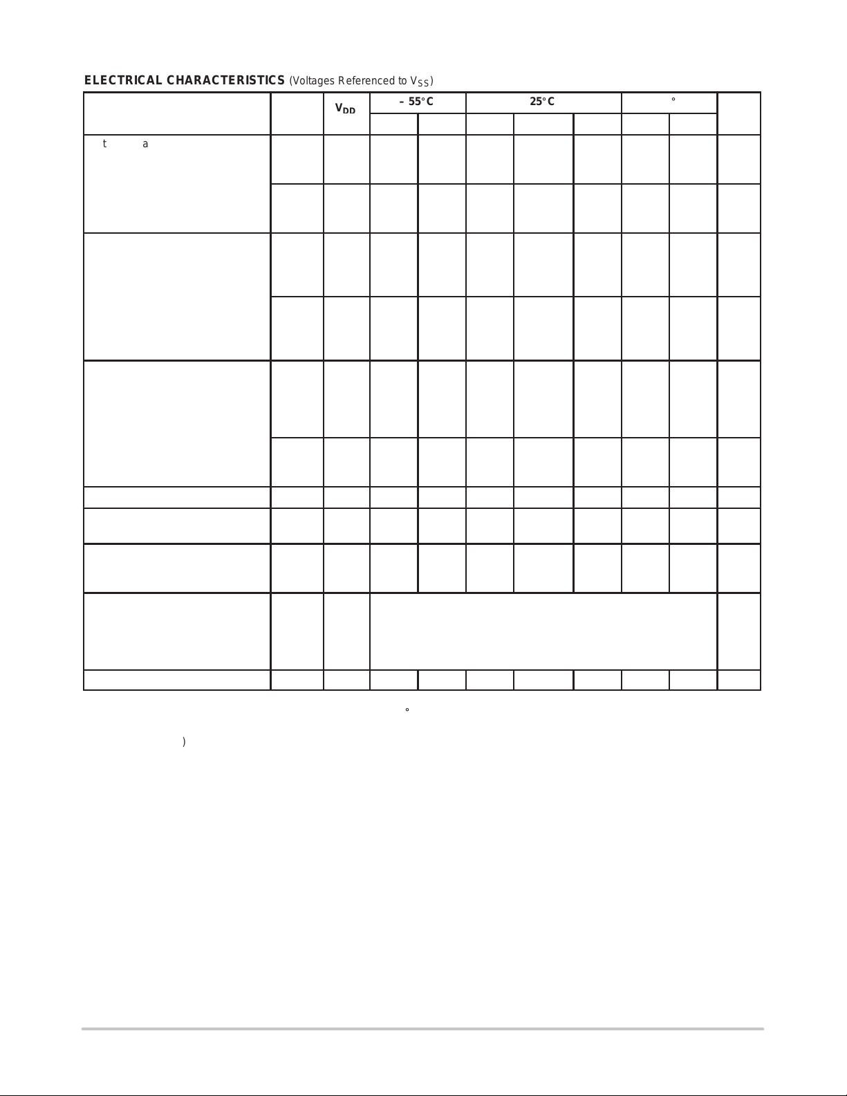
ELECTRICAL CHARACTERISTICS (Voltages Referenced to V
V
Characteristic Symbol
Output Voltage “0” Level
= VDD or 0
V
in
“1” Level
V
= 0 or V
in
DD
Input Voltage “0” Level
(V
= 4.5 or 0.5 Vdc)
O
= 9.0 or 1.0 Vdc)
(V
O
(V
= 13.5 or 1.5 Vdc)
O
“1” Level
= 0.5 or 4.5 Vdc)
(V
O
(V
= 1.0 or 9.0 Vdc)
O
= 1.5 or 13.5 Vdc)
(V
O
Output Drive Current
(V
= 2.5 Vdc) Source
OH
= 4.6 Vdc)
(V
OH
(V
= 9.5 Vdc)
OH
(V
= 13.5 Vdc)
OH
(VOL = 0.4 Vdc) Sink
(V
= 0.5 Vdc)
OL
(V
= 1.5 Vdc)
OL
Input Current I
Input Capacitance
(V
= 0)
in
Quiescent Current
(Per Package)
Total Supply Current
(4.) (5.)
(Dynamic plus Quiescent,
Per Package)
= 50 pF on all outputs, all
(C
L
V
OL
V
OH
V
V
I
OH
I
OL
in
C
I
DD
I
Vdc
5.0
10
15
5.0
10
15
IL
5.0
10
15
IH
5.0
10
15
5.0
5.0
10
15
5.0
10
15
Min Max Min Typ
—
—
—
4.95
9.95
14.95
—
—
—
3.5
7.0
11
– 3.0
– 0.64
– 1.6
– 4.2
0.64
1.6
4.2
15 — ± 0.1 — ±0.00001 ± 0.1 — ± 1.0 µAdc
in
T
— — — — 5.0 7.5 — — pF
5.0
10
15
—
—
—
5.0
10
15
)
SS
– 55_C 25_C 125_C
(3.)
Max Min Max
0.05
0.05
0.05
—
—
—
1.5
3.0
4.0
—
—
—
—
—
—
—
—
—
—
5.0
10
20
—
—
—
4.95
9.95
14.95
—
—
—
3.5
7.0
11
– 2.4
– 0.51
– 1.3
– 3.4
0.51
1.3
3.4
—
—
—
0
0
0
5.0
10
15
2.25
4.50
6.75
2.75
5.50
8.25
– 4.2
– 0.88
– 2.25
– 8.8
0.88
2.25
8.8
0.005
0.010
0.015
IT = (4.2 µA/kHz) f + I
IT = (8.8 µA/kHz) f + I
IT = (13.7 µA/kHz) f + I
0.05
0.05
0.05
—
—
—
1.5
3.0
4.0
—
—
—
—
—
—
—
—
—
—
5.0
10
20
DD
DD
DD
—
—
—
4.95
9.95
14.95
—
—
—
3.5
7.0
11
– 1.7
– 0.36
– 0.9
– 2.4
0.36
0.9
2.4
—
—
—
0.05
0.05
0.05
buffers switching)
Three–State Leakage Current I
TL
15 — ± 0.1 — ± 0.0001 ± 0.1 — ± 3.0 µAdc
3. Data labelled “Typ” is not to be used for design purposes but is intended as an indication of the IC’s potential performance.
4. The formulas given are for the typical characteristics only at 25_C.
5. To calculate total supply current at loads other than 50 pF:
I
) = IT(50 pF) + (CL – 50) Vfk
T(CL
where: I
is in µA (per package), CL in pF, V = (VDD – VSS) in volts, f in kHz is input frequency, and k = 0.004.
T
—
—
—
1.5
3.0
4.0
—
—
—
—
—
—
—
—
—
—
150
300
600
Unit
Vdc
Vdc
Vdc
Vdc
mAdc
mAdc
µAdc
µAdc
http://onsemi.com
3
Page 4

MC14517B
SWITCHING CHARACTERISTICS
(6.)
(C
L
= 50 pF, T
Characteristic
Output Rise and Fall Time
t
, t
TLH
t
TLH
t
TLH
= (1.5 ns/pF) CL + 25 ns
THL
, t
= (0.75 ns/pF) CL + 12.5 ns
THL
, t
= (0.65 ns/pF) CL + 9.5 ns
THL
Propagation Delay Time
t
, t
PLH
t
PLH
t
PLH
= (1.7 ns/pF) CL + 390 ns
PHL
, t
= (0.66 ns/pF) CL + 177 ns
PHL
, t
= (0.5 ns/pF) CL + 115 ns
PHL
Clock Pulse Width t
Clock Pulse Frequency f
Clock Pulse Rise and Fall Time t
= 25_C)
A
Symbol V
t
, t
TLH
THL
t
, t
PLH
PHL
WH
cl
, t
TLH
THL
5.0
10
15
5.0
10
15
5.0
10
15
5.0
10
15
5.0
10
DD
Min Typ
—
100
—
—
—
—
—
330
475
210
140
170
125
100
—
—
—
3.0
6.7
8.3
See Note
50
40
75
60
(7.)
(8.)
Max Unit
ns
200
100
80
ns
770
300
215
—
ns
—
—
1.5
MHz
4.0
5.3
—
15
Data to Clock Setup Time t
Data to Clock Hold Time t
Write Enable to Clock Setup Time t
Write Enable to Clock Release Time t
su
h
su
rel
5.0
10
15
5.0
10
15
5.0
10
15
5.0
10
15
0
10
15
150
75
35
400
200
110
380
180
100
– 40
– 15
0
75
25
10
170
65
50
160
55
40
—
ns
—
—
—
ns
—
—
—
ns
—
—
—
ns
—
—
6. The formulas given are for the typical characteristics only at 25_C.
7. Data labelled “Typ” is not to be used for design purposes but is intended as an indication of the IC’s potential performance.
8. When shift register sections are cascaded, the maximum rise and fall time of the clock input should be equal to or less than the rise and fall
time of the data outputs, driving data inputs, plus the propagation delay of the output driving stage.
f
o
C
D
(f = 1/2 fo)
REPETITIVE WAVEFORM
Figure 1. Power Dissipation Test Circuit and Waveform
D
C
V
DD
V
SS
V
DD
V
SS
50 µF
http://onsemi.com
4
V
DD
Q16 Q32 Q48 Q64
D
C
C
L
C
L
C
L
WE
C
L
D
C
WE
Q16 Q32 Q48 Q64
V
SS
I
D
CLCLCLC
L
Page 5

VDD = V
t
MC14517B
V
= V
out
OH
GS
VDD = V
GS
V
= V
out
OL
Q16 Q32 Q48 Q64
D
C
WE
D
C
WE
Q16 Q32 Q48 Q64
V
SS
(Output being tested should be in the high–logic state)
Figure 2. Typical Output Source Current
Characteristics T est Circuit
WH
t
PIN NO’S
CLOCK 4 (12)
WRITE 3 (13)
t
su1
DATA IN 7 (9)
t
su1
16–BIT OUTPUT 1 (15)
17–BIT INPUT
t
su1
32–BIT OUTPUT 6 (10)
33–BIT INPUT
t
su1
48–BIT OUTPUT 2 (14)
49–BIT INPUT
64–BIT OUTPUT 5 (11)
WL
1221617181933
t
h1
t
h1
t
h1
t
h1
t
t
t
t
t
t
t
t
h0
su0
50%
su0
h0
su0
h0
su0
h0
D
C
WE
D
I
OH
C
WE
EXTERNAL
POWER
SUPPLY
V
SS
(Output being tested should be in the low–logic state)
t
rel
20 ns
t
PHL
V
DD
20 ns
V
DD
20 ns
V
DD
20 ns
t
t
t
PHL
PHL
PHL
t
t
PLH
PLH
Figure 4. AC Test Waveforms
Q16 Q32 Q48 Q64
Q16 Q32 Q48 Q64
Figure 3. Typical Output Sink Current
Characteristics T est Circuit
90%
10%
t
su
t
t
PLH
PLH
90%
90%
t
TLH
90%
t
TLH
t
TLH
t
TLH
10%
V
OH
10%
V
OH
50%
10%
V
OH
t
THL
t
t
t
THL
THL
THL
50%
V
V
V
OL
OL
OL
I
OL
EXTERNAL
POWER
SUPPLY
50%
V
DD
V
SS
V
DD
V
SS
V
DD
V
SS
V
DD
V
SS
V
DD
V
SS
V
DD
V
SS
V
DD
V
SS
CLOCK
DATA
WRITE
ENABLE
EXPANDED BLOCK DIAGRAM (1/2 OF DEVICE SHOWN)
D
1
C
WRITE ENABLE = 0, 16–BIT OUTPUT
WRITE ENABLE = 1, 17–BIT INPUT
D
Q
2
C
D
Q
C
3–STATE
16
17
C
D
Q
WE
D
Q
32
C
3–STATE
32–BIT OUTPUT
33–BIT INPUT
D
Q
33
C
WE
D
Q
48
C
3–STATE
48–BIT OUTPUT
49–BIT INPUT
D
Q
49
C
WE
Q
D
64
C
3–STATE
Q
64–BIT OUTPUT
HIGH IMPEDANCE
http://onsemi.com
5
Page 6

P ACKAGE DIMENSIONS
PLASTIC DIP PACKAGE
–A–
916
B
18
F
H
G
D
16 PL
0.25 (0.010) T
C
S
SEATING
–T–
PLANE
K
M
A
MC14517B
PDIP–16
P SUFFIX
CASE 648–08
ISSUE R
J
M
NOTES:
1. DIMENSIONING AND TOLERANCING PER ANSI
Y14.5M, 1982.
2. CONTROLLING DIMENSION: INCH.
3. DIMENSION L TO CENTER OF LEADS WHEN
FORMED PARALLEL.
4. DIMENSION B DOES NOT INCLUDE MOLD FLASH.
5. ROUNDED CORNERS OPTIONAL.
DIM MIN MAX MIN MAX
L
M
A 0.740 0.770 18.80 19.55
B 0.250 0.270 6.35 6.85
C 0.145 0.175 3.69 4.44
D 0.015 0.021 0.39 0.53
F 0.040 0.70 1.02 1.77
G 0.100 BSC 2.54 BSC
H 0.050 BSC 1.27 BSC
J 0.008 0.015 0.21 0.38
K 0.110 0.130 2.80 3.30
L 0.295 0.305 7.50 7.74
M 0 10 0 10
S 0.020 0.040 0.51 1.01
MILLIMETERSINCHES
____
http://onsemi.com
6
Page 7

MC14517B
P ACKAGE DIMENSIONS
SOIC–16
DW SUFFIX
PLASTIC SOIC PACKAGE
CASE 751G–03
ISSUE B
16 9
M
B
H8X
M
0.25
0.25 B
14X
D
B16X
M
S
A
T
e
A
q
NOTES:
1. DIMENSIONS ARE IN MILLIMETERS.
2. INTERPRET DIMENSIONS AND TOLERANCES
PER ASME Y14.5M, 1994.
E
_
h X 45
81
B
S
A
L
A1
SEATING
PLANE
T
C
3. DIMENSIONS D AND E DO NOT INLCUDE MOLD
PROTRUSION.
4. MAXIMUM MOLD PROTRUSION 0.15 PER SIDE.
5. DIMENSION B DOES NOT INCLUDE DAMBAR
PROTRUSION. ALLOWABLE DAMBAR
PROTRUSION SHALL BE 0.13 TOTAL IN EXCESS
OF THE B DIMENSION AT MAXIMUM MATERIAL
CONDITION.
MILLIMETERS
DIM MIN MAX
A 2.35 2.65
A1 0.10 0.25
B 0.35 0.49
C 0.23 0.32
D 10.15 10.45
E 7.40 7.60
e 1.27 BSC
H 10.05 10.55
h 0.25 0.75
L 0.50 0.90
q
0 7
__
http://onsemi.com
7
Page 8

MC14517B
ON Semiconductor and are trademarks of Semiconductor Components Industries, LLC (SCILLC). SCILLC reserves the right to make changes
without further notice to any products herein. SCILLC makes no warranty , representation or guarantee regarding the suitability of its products for any particular
purpose, nor does SCILLC assume any liability arising out of the application or use of any product or circuit, and specifically disclaims any and all liability ,
including without limitation special, consequential or incidental damages. “Typical” parameters which may be provided in SCILLC data sheets and/or
specifications can and do vary in different applications and actual performance may vary over time. All operating parameters, including “Typicals” must be
validated for each customer application by customer’s technical experts. SCILLC does not convey any license under its patent rights nor the rights of others.
SCILLC products are not designed, intended, or authorized for use as components in systems intended for surgical implant into the body, or other applications
intended to support or sustain life, or for any other application in which the failure of the SCILLC product could create a situation where personal injury or
death may occur. Should Buyer purchase or use SCILLC products for any such unintended or unauthorized application, Buyer shall indemnify and hold
SCILLC and its officers, employees, subsidiaries, affiliates, and distributors harmless against all claims, costs, damages, and expenses, and reasonable
attorney fees arising out of, directly or indirectly , any claim of personal injury or death associated with such unintended or unauthorized use, even if such claim
alleges that SCILLC was negligent regarding the design or manufacture of the part. SCILLC is an Equal Opportunity/Affirmative Action Employer .
PUBLICATION ORDERING INFORMATION
NORTH AMERICA Literature Fulfillment:
Literature Distribution Center for ON Semiconductor
P.O. Box 5163, Denver, Colorado 80217 USA
Phone: 303–675–2175 or 800–344–3860 Toll Free USA/Canada
Fax: 303–675–2176 or 800–344–3867 Toll Free USA/Canada
Email: ONlit@hibbertco.com
Fax Response Line: 303–675–2167 or 800–344–3810 T oll Free USA/Canada
N. American Technical Support: 800–282–9855 Toll Free USA/Canada
EUROPE: LDC for ON Semiconductor – European Support
German Phone: (+1) 303–308–7140 (M–F 1:00pm to 5:00pm Munich Time)
Email: ONlit–german@hibbertco.com
French Phone: (+1) 303–308–7141 (M–F 1:00pm to 5:00pm Toulouse T ime)
Email: ONlit–french@hibbertco.com
English Phone: (+1) 303–308–7142 (M–F 12:00pm to 5:00pm UK Time)
Email: ONlit@hibbertco.com
EUROPEAN TOLL–FREE ACCESS*: 00–800–4422–3781
*Available from Germany, France, Italy, England, Ireland
CENTRAL/SOUTH AMERICA:
Spanish Phone: 303–308–7143 (Mon–Fri 8:00am to 5:00pm MST)
Email: ONlit–spanish@hibbertco.com
ASIA/PACIFIC : LDC for ON Semiconductor – Asia Support
Phone: 303–675–2121 (Tue–Fri 9:00am to 1:00pm, Hong Kong Time)
T oll Free from Hong Kong & Singapore:
001–800–4422–3781
Email: ONlit–asia@hibbertco.com
JAPAN: ON Semiconductor, Japan Customer Focus Center
4–32–1 Nishi–Gotanda, Shinagawa–ku, T okyo, Japan 141–8549
Phone: 81–3–5740–2745
Email: r14525@onsemi.com
ON Semiconductor Website: http://onsemi.com
For additional information, please contact your local
Sales Representative.
http://onsemi.com
8
MC14517B/D
 Loading...