

Page 1
MC145166•MC145167MOTOROLA
1
CMOS
These devices are dual phase–locked loop (PLL) frequency synthesizers in–
tended for use primarily in 46/49 MHz cordless phones with up to 10 channels.
These parts contain two mask–programmable counter ROMs for receive and
transmit loops with two independent phase detect circuits. A common reference
oscillator and reference divider are shared by the receive and transmit circuits.
Frequency selection is accomplished via a 4–bit parallel input for the
MC145166. The MC145167 utilizes a serial interface.
Other features include a lock detect circuit for the transmit loop, illegal code
default, and a 5 kHz tone output.
• Synthesizes Up to Ten Channel Pairs
• Maximum Operating Frequency: 60 MHz @ V
in
= 200 mV p–p
• Operating Temperature Range: – 40 to + 75°C
• Operating Voltage Range: 2.5 to 5.5 V
• On–Chip Oscillator Circuit Supports External Crystal
• Lock Detect Signal
• Operating Power Consumption: 3.0 mA @ 3.0 V
• Standby Mode for Power Savings: 1.5 mA @ 3.0 V
• Also See MC145162
Order this document
by MC145166/D
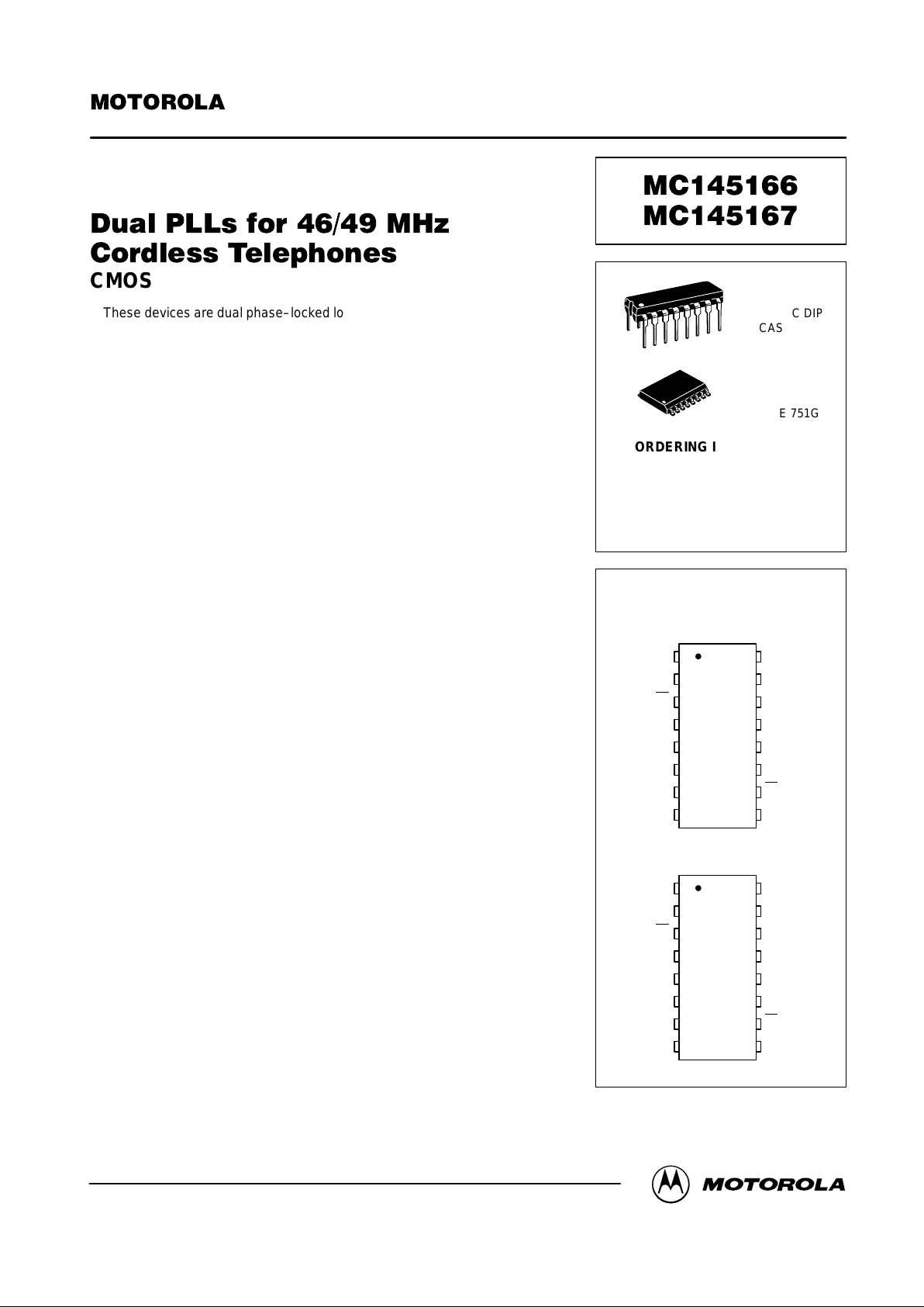
SEMICONDUCTOR TECHNICAL DATA
P SUFFIX
PLASTIC DIP
CASE 648
DW SUFFIX
SOG PACKAGE
CASE 751G
ORDERING INFORMATION
MC145166P Plastic DIP
MC145166DW SOG Package
MC145167P Plastic DIP
MC145167DW SOG Package
16
1
16
1
PIN ASSIGNMENTS
MC145166P
MC145166DW
13
14
15
16
9
10
11
125
4
3
2
1
8
7
6
V
SS
PD1
f
in1
V
DD
OSC
in
f
in2
LD
PD2
5 k
SB
MODE
OSC
out
D3
D2
D1
D0
MC145167P
MC145167DW
13
14
15
16
9
10
11
125
4
3
2
1
8
7
6
V
SS
PD1
f
in1
V
DD
OSC
in
f
in2
LD
PD2
5 k
SB
MODE
OSC
out
ENB
NC
CLK
DATA
NC = NO CONNECTION
Motorola, Inc. 1998
REV 2
1/98 TN98011400
Page 2
MC145166•MC145167 MOTOROLA
2
BLOCK DIAGRAM
*On–chip pull–down.
OSC
out
OSC
in
f
in2
f
in1
DATA
CLK
ENB
4–BIT S/R
4–BIT LATCH
D3
D2
D1
D0
MODE
PD2
V
DD
PD1
f
v
=
5 kHz
DECODE
LOGIC
PHASE
DET 2
LOCK
DET
PHASE
DET 1
14
13
REFERENCE
COUNTER
DIVIDE–BY–2048
14–BIT
DIVIDE–BY–N
TRANSMIT
COUNTER
13–BIT DIVIDE–BY–N
RECEIVE COUNTER
SB
RECEIVE
ROM
TRANSMIT
ROM
*
5 kHz
f
v
LD
f
r
*
*
*
*
MC145166
ONLY
MC145167 ONLY
f
r
V
SS
5 k
Page 3
MC145166•MC145167MOTOROLA
3
MAXIMUM RATINGS* (Voltages Referenced to V
SS
)
Symbol Rating Value Unit
V
DD
DC Supply Voltage – 0.5 to + 6.0 V
V
in
Input Voltage, All Inputs – 0.5 to VDD + 0.5 V
Iin, I
out
DC Current Drain Per Pin 10 mA
IDD, ISSDC Current Drain VDD or VSS Pins 30 mA
T
stg
Storage Temperature Range – 65 to + 150 °C
*Maximum Ratings are those values beyond which damage to the device may occur.
Functional operation should be restricted to the limits in the Electrical Characteristics
tables or Pin Descriptions section.
ELECTRICAL CHARACTERISTICS (Voltages Referenced to V
SS
, TA = 25°C)
Guaranteed Limit
Symbol Characteristic V
DD
Min Max
Unit
V
DD
Power Supply Voltage Range — 2.5 5.5 V
V
OL
Output Voltage 0 Level
(I
out
= 0)
2.5
5.5
—
—
0.05
0.05
V
V
OH
(Vin = VDD or 0) 1 Level 2.5
5.5
2.45
5.45
—
—
V
IL
Input Voltage 0 Level
(V
out
= 0.5 V or VDD – 0.5 V)
2.5
5.5
—
—
0.75
1.65
V
V
IH
1 Level 2.5
5.5
1.75
3.85
—
—
I
OH
Output Current (V
out
= 2.2 V) Source
(V
out
= 5.0 V)
2.5
5.5
– 0.18
– 0.55
—
—
mA
I
OL
(V
out
= 0.3 V) Sink
(V
out
= 0.5 V)
2.5
5.5
0.18
0.55
—
—
I
IL
Input Current OSCin, f
in1
, f
in2
(Vin = 0)
2.5
5.5
—
—
– 30
– 66
µA
DATA, SB, Mode 2.5
5.5
—
—
– 0.05
– 0.11
I
IH
(Vin = VDD – 0.5) OSCin, f
in1
, f
in2
2.5
5.5
—
—
30
66
µA
DATA, SB, Mode 2.5
5.5
—
—
50
121
C
in
Input Capacitance — — 14.0 pF
C
out
Output Capacitance — — 8.0 pF
I
DD
Standby Current, SB = VSS or Open 2.5
5.5
—
—
1.4
3.6
mA
I
dd
Operating Current
(200 mV p–p input at f
in1
and f
in2
, SB
= VDD)
2.5
5.5
—
—
2.8
6.2
mA
I
OZ
Three–State Leakage Current
(V
out
= 0 or 5.5 V)
5.5 — ± 1.0 µA
This device contains protection circuitry to
guard against damage due to high static voltages or electric fields. However, precautions
must be taken to avoid applications of any
voltage higher than maximum rated voltages
to this high–impedance circuit. For proper operation, Vin and V
out
should be constrained to
the range VSS≤ (Vin or V
out
) ≤ VDD.
Unused inputs must always be tied to an
appropriate logic voltage level (e.g., either V
SS
or VDD). Unused outputs must be left open.
Page 4
MC145166•MC145167 MOTOROLA
4
SWITCHING CHARACTERISTICS (T
A
= 25°C, CL = 50 pF)
Figure
Guaranteed Limit
Symbol Characteristic
Figure
No.
V
DD
Min Max
Unit
t
TLH
Output Rise Time 1, 5 3.0
5.0
—
—
200
100
ns
t
THL
Output Fall Time 1, 5 3.0
5.0
—
—
200
100
ns
tr, t
f
Input Rise and Fall Time, OSC
in
2 3.0
5.0
—
—
5.0
4.0
µs
f
max
Input Frequency OSC
in
Input = Sine Wave 200 mV p–p f
in1
f
in2
3.0 – 5.0
3.0 – 5.0
3.0 – 5.0
—
—
—
12
60
60
MHz
t
su
Setup Time (MC145167) DATA to CLK 3 3.0
5.0
100
50
—
—
ns
ENB to CLK 3.0
5.0
200
100
—
—
t
h
Hold Time (MC145167), CLK to DATA 3 3.0
5.0
80
40
—
—
ns
t
rec
Recovery Time (MC145167), ENB to CLK 3 3.0
5.0
80
40
—
—
ns
t
w
Input Pulse Width (MC145167), CLK and ENB 4 3.0
5.0
80
60
—
—
ns
Page 5

MC145166•MC145167MOTOROLA
5
SWITCHING W AVEFORMS
DATA
CLK
ENB
D3
50%
t
su
t
h
FIRST
CLK
D2 D1 D0
LAST
CLK
t
rec
50%
PREVIOUS
DATA LATCHED
FIRST
CLK
t
su
t
TLH
ANY
OUTPUT
90%
10%
t
THL
ENB,
CLK
50%
t
w
t
r
t
f
90%
10%
OSCin, f
in
Figure 1. Figure 2.
Figure 3.
Figure 4.
Page 6

MC145166•MC145167 MOTOROLA
6
PIN DESCRIPTIONS
INPUT PINS
OSCin/OSC
out
Reference Oscillator Input/Output (Pins 1,16)
These pins form a reference oscillator when connected to
an external parallel–resonant crystal. For a 46/49 MHz cordless phone application, a 10.24 MHz crystal is needed.
OSCin may also serve as input for an externally generated
reference signal. This signal is typically ac coupled to
OSCin, but for larger amplitude signals (standard CMOS
logic levels) dc coupling may also be used. In the external
reference mode, no connection is required for OSC
out
.
MODE
Mode Select (Pin 2)
Mode is for determining whether the part is to be used in
the base or handset of a cordless phone. Internally, this pin is
used in the decoding logic for selecting the ROM address.
When high, the device is set in the base mode, and when
low, it is set in the handset mode. This input has an internal
pull–down device.
SB
Standby Input (Pin 3)
The standby pin is used to save power when not transmitting. When high, both the transmit and receive loops are in
operation. When low, the transmit loop is disabled, thereby
reducing power consumption. This input has an internal pull–
down device.
D0 – D3
Data Inputs (MC145166 — Pins 5 – 8)
These inputs provide the BCD code for selecting the one
of ten channels to be locked in both the transmit and receive
loop. When address data other than 1 – 10 are input, the decoding logic defaults to channel 10. The frequency assignments with reference to Mode and D0 – D3 are shown in
Table 1. These inputs have internal pull–down devices.
f
in1
, f
in2
Frequency Inputs (Pins 14, 9)
f
in1
and f
in2
are inputs to the divide–by–N receive and
transmit counters, respectively. These signals are typically
derived from the loop VCO and are ac coupled. For larger
amplitude signals (standard CMOS logic levels), dc coupling
may be used. The minimum input level is 200 mV p–p.
CLK, DATA
Clock, Data (MC145167 — Pins 5, 6)
These pins provide the BCD input by using serial channel
programming instead of parallel. Logical high represents a 1.
Each low–to–high transition of the clock shifts one bit of data
into the on–chip shift register.
ENB
Enable (MC145167 — Pin 8)
The enable pin controls the data transfer from the shift register to the 4–bit latch. A positive pulse latches the data.
OUTPUT PINS
5 k
5 kHz Tone Signals (Pin 4)
The 5 kHz tone signals are N–channel, open–drain outputs derived from the reference oscillator.
LD
Lock Detect Signal (Pin 10)
The lock detect signal is associated with the transmit loop.
The lock output goes high to indicate an out–of–lock condition. This is a P–channel open–drain output.
PD1, PD2
Phase Detector Outputs (Pins 13, 11)
These are three–state outputs of the transmit and receive
phase detectors for use as loop error signals. Phase detector
gain is VDD/4 π volts per radian.
Frequency fv > fr or fv leading: Output = Negative pulses
Frequency fv < fr or fv lagging: Output = Positive pulses
Frequency fv = fr and phase coincidence: Output = High–
impedance state
POWER SUPPLY
V
SS
Negative Power Supply (Pin 12)
This pin is the negative supply potential and is usually
ground.
V
DD
Positive Power Supply (Pin 15)
This pin is the positive supply potential and may range
from + 2.5 to + 5.5 V with respect to VSS.
Page 7

MC145166•MC145167MOTOROLA
7
Table 1. MC145166/67 Divide Ratios and VCO Frequencies
Handset (Mode = 0) Base (Mode = 1)
Channels Transmit Receive Transmit Receive
D3 D2 D1 D0 CH# f
in2
(MHz)
N
f
in1
(MHz)
N
f
in2
(MHz)
N
f
in1
(MHz)
N
0
0
0
0
0
0
0
1
1
1
0
0
0
1
1
1
1
0
0
0
0
1
1
0
0
1
1
0
0
1
1
0
1
0
1
0
1
0
1
0
1
2
3
4
5
6
7
8
9
10
49.670
49.845
49.860
49.770
49.875
49.830
49.890
49.930
49.990
49.970
9934
9969
9972
9954
9975
9966
9978
9986
9998
9994
35.915
35.935
35.975
36.015
36.035
36.075
36.135
36.175
36.235
36.275
7183
7187
7195
7203
7207
7215
7227
7235
7247
7255
46.610
46.630
46.670
46.710
46.730
46.770
46.830
46.870
46.930
46.970
9322
9326
9334
9342
9346
9354
9366
9374
9386
9394
38.975
39.150
39.165
39.075
39.180
39.135
39.195
39.235
39.295
39.275
7795
7830
7833
7815
7836
7827
7839
7847
7859
7855
NOTES:
1. Other input combinations will be defaulted to channel 10.
2. 0 = logic low, 1 = logic high.
Page 8

MC145166•MC145167 MOTOROLA
8
Figure 5. MC145166 Circuit Example
2.7 k
Ω
47 k
Ω
100 k
Ω
10 µF
68 pF
0.01 µF
27 pF
47 pF
33 pF
1N5462A
MPS9426C
3.3 k
Ω
8 pF
39 k
Ω
1 k
Ω
VCC (3.6 V)
1.2 k
Ω
12 pF
TO 1ST
MIXER
68 k
Ω
MPS9426C
10 pF
10.24 MHz
TO 2ND
MIXER
3 pF
1
15
6
7
8
12
OSC
out
OSC
in
V
DD
D0
D1
D2
D3
V
SS
f
in1
PD1
PD2
LD
f
in2
MC145166
LOCK DETECT (LD)
ENABLE
RF Tx AMP
33 pF
0.01
µ
F
100 k
Ω
1 k
Ω
1 k
Ω
10 pF
39 k
Ω
0.01 µF 10 µF
10 pF
27 pF
47 pF
8 pF
3.3 k
Ω
33 pF
MPS9426C MPS9426C 1N5462A
1
µ
F
47 kW
100 k
Ω
2.7 k
Ω
TO PIN 1
OF
MC2831A
1
µ
F
V+
V+
0.01 µF
9
10
11
13
14
16
Page 9

MC145166•MC145167MOTOROLA
9
Figure 6. DPLL Application in 46/49 MHz Cordless Phone
FILTER
RF
1ST
MIX
2ND
MIX
10.695 MHz 0.455 MHz
10.24 MHz
38.975 MHz
Rx
VCO
f
46.610 MHz
FILTER
RF
Tx
VCO
AMP
BUF
AMP
MIC
DIALING
DC
OSC
out
10.24 MHz
OSC
in
AMP
OSC
MC145166
5 kHz
5 kHz
11 BITS
5 kHz
14 BITS
MODE D3
ROM
PD–R
5 kHz
PD–T
LP FILTER
D2 D1 D0
V
SS LD
V
DD
PROG A
PRESCALER
PHASE
DET
A
REF
COUNTER
PROG B
PRESCALER
PHASE
DET
B
LOCK
DET
46.610 MHz
49.670 MHz
in
–R
f
in
–T
LP FILTER
Page 10

MC145166•MC145167 MOTOROLA
10
P ACKAGE DIMENSIONS
P SUFFIX
PLASTIC DIP
CASE 648–08
NOTES:
1. DIMENSIONING AND TOLERANCING PER ANSI
Y14.5M, 1982.
2. CONTROLLING DIMENSION: INCH.
3. DIMENSION L TO CENTER OF LEADS WHEN
FORMED PARALLEL.
4. DIMENSION B DOES NOT INCLUDE MOLD FLASH.
5. ROUNDED CORNERS OPTIONAL.
–A–
B
F
C
S
H
G
D
J
L
M
16 PL
SEATING
18
916
K
PLANE
–T–
M
A
M
0.25 (0.010) T
DIM MIN MAX MIN MAX
MILLIMETERSINCHES
A 0.740 0.770 18.80 19.55
B 0.250 0.270 6.35 6.85
C 0.145 0.175 3.69 4.44
D 0.015 0.021 0.39 0.53
F 0.040 0.70 1.02 1.77
G 0.100 BSC 2.54 BSC
H 0.050 BSC 1.27 BSC
J 0.008 0.015 0.21 0.38
K 0.110 0.130 2.80 3.30
L 0.295 0.305 7.50 7.74
M 0 10 0 10
S 0.020 0.040 0.51 1.01
____
DW SUFFIX
SOG PACKAGE
CASE 751G–02
DIM MIN MAX MIN MAX
INCHESMILLIMETERS
A 10.15 10.45 0.400 0.411
B 7.40 7.60 0.292 0.299
C 2.35 2.65 0.093 0.104
D 0.35 0.49 0.014 0.019
F 0.50 0.90 0.020 0.035
G 1.27 BSC 0.050 BSC
J 0.25 0.32 0.010 0.012
K 0.10 0.25 0.004 0.009
M 0 7 0 7
P 10.05 10.55 0.395 0.415
R 0.25 0.75 0.010 0.029
M
B
M
0.010 (0.25)
NOTES:
1. DIMENSIONING AND TOLERANCING PER ANSI
Y14.5M, 1982.
2. CONTROLLING DIMENSION: MILLIMETER.
3. DIMENSIONS A AND B DO NOT INCLUDE MOLD
PROTRUSION.
4. MAXIMUM MOLD PROTRUSION 0.15 (0.006) PER
SIDE.
5. DIMENSION D DOES NOT INCLUDE DAMBAR
PROTRUSION. ALLOWABLE DAMBAR
PROTRUSION SHALL BE 0.13 (0.005) TOTAL IN
EXCESS OF D DIMENSION AT MAXIMUM
MATERIAL CONDITION.
–A–
–B– P8X
G14X
D16X
SEATING
PLANE
–T–
S
A
M
0.010 (0.25) B
S
T
16 9
81
F
J
R
X 45
_
____
M
C
K
Page 11

MC145166•MC145167MOTOROLA
11
Motorola reserves the right to make changes without further notice to any products herein. Motorola makes no warranty , representation or guarantee regarding
the suitability of its products for any particular purpose, nor does Motorola assume any liability arising out of the application or use of any product or circuit, and
specifically disclaims any and all liability, including without limitation consequential or incidental damages. “T ypical” parameters which may be provided in Motorola
data sheets and/or specifications can and do vary in different applications and actual performance may vary over time. All operating parameters, including “Typicals”
must be validated for each customer application by customer’s technical experts. Motorola does not convey any license under its patent rights nor the rights of
others. Motorola products are not designed, intended, or authorized for use as components in systems intended for surgical implant into the body, or other
applications intended to support or sustain life, or for any other application in which the failure of the Motorola product could create a situation where personal injury
or death may occur. Should Buyer purchase or use Motorola products for any such unintended or unauthorized application, Buyer shall indemnify and hold Motorola
and its officers, employees, subsidiaries, affiliates, and distributors harmless against all claims, costs, damages, and expenses, and reasonable attorney fees
arising out of, directly or indirectly, any claim of personal injury or death associated with such unintended or unauthorized use, even if such claim alleges that
Motorola was negligent regarding the design or manufacture of the part. Motorola and are registered trademarks of Motorola, Inc. Motorola, Inc. is an Equal
Opportunity/Affirmative Action Employer.
Mfax is a trademark of Motorola, Inc.
How to reach us:
USA/EUROPE /Locations Not Listed: Motorola Literature Distribution; JAPAN: Nippon Motorola Ltd.: SPD, Strategic Planning Office, 141,
P.O. Box 5405, Denver, Colorado 80217. 1–303–675–2140 or 1–800–441–2447 4–32–1 Nishi–Gotanda, Shagawa–ku, Tokyo, Japan. 03–5487–8488
Mfax: RMFAX0@email.sps.mot.com – TOUCHTONE 1–602–244–6609 ASIA/PACIFIC: Motorola Semiconductors H.K. Ltd.; 8B Tai Ping Industrial Park,
Moto rola Fax Back System – US & Canada ONLY 1–800–774–1848 51 T ing Kok Road, Tai Po, N.T., Hong Kong. 852–26629298
– http://sps.motorola.com/mfax/
HOME PAGE: http://motorola.com/sps/ CUSTOMER FOCUS CENTER: 1–800–521–6274
MC145166/D
◊
 Loading...