

Datasheet MC14515BDWR2, MC14515BCP, MC14514BCP, MC14514BDW, MC14514BDWR2 Datasheet (MOTOROLA)
...Page 1
MC14514B, MC14515B
4-Bit Transparent
Latch/4-to-16 Line Decoder
The MC14514B and MC14515B are two output options of a 4 to 16
line decoder with latched inputs. The MC14514B (output active high
option) presents a logical “1” at the selected output, whereas the
MC14515B (output active low option) presents a logical “0” at the
selected output. The latches are R–S type flip–flops which hold the
last input data presented prior to the strobe transition from “1” to “0”.
These high and low options of a 4–bit latch/4 to 16 line decoder are
constructed with N–channel and P–channel enhancement mode
devices in a single monolithic structure. The latches are R–S type
flip–flops and data is admitted upon a signal incident at the strobe
input, decoded, and presented at the output.
These complementary circuits find primary use in decoding
applications where low power dissipation and/or high noise immunity
is desired.
• Supply Voltage Range = 3.0 Vdc to 18 Vdc
• Capable of Driving T wo Low–power TTL Loads or One Low–power
Schottky TTL Load Over the Rated T emperature Range
http://onsemi.com
PDIP–24
P SUFFIX
CASE 709
24
MC145XXBCP
1
MARKING
DIAGRAMS
AWLYYWW
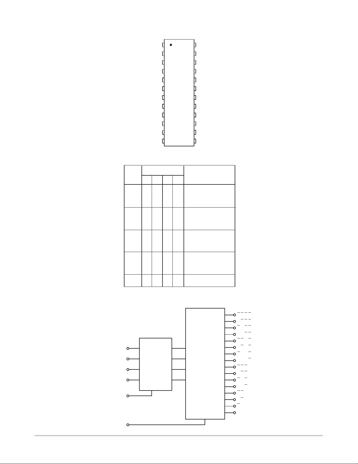
MAXIMUM RATINGS (Voltages Referenced to V
Symbol Parameter Value Unit
V
DD
Vin, V
Iin, I
P
T
T
stg
T
1. Maximum Ratings are those values beyond which damage to the device
may occur.
2. Temperature Derating:
Plastic “P and D/DW” Packages: – 7.0 mW/_C From 65_C To 125_C
This device contains protection circuitry to guard against damage due to high
static voltages or electric fields. However, precautions must be taken to avoid
applications of any voltage higher than maximum rated voltages to this
high–impedance circuit. For proper operation, V
to the range V
Unused inputs must always be tied to an appropriate logic voltage level (e.g.,
either V
DC Supply Voltage Range –0.5 to +18.0 V
Input or Output Voltage Range
out
out
D
A
L
(DC or Transient)
Input or Output Current
(DC or Transient) per Pin
Power Dissipation,
per Package (Note 2.)
Ambient Temperature Range –55 to +125 °C
Storage Temperature Range –65 to +150 °C
Lead Temperature
(8–Second Soldering)
v (Vin or V
SS
or VDD). Unused outputs must be left open.
SS
) v VDD.
out
) (Note 1.)
SS
–0.5 to VDD + 0.5 V
±10 mA
500 mW
260 °C
and V
in
should be constrained
out
24
SOIC–24
DW SUFFIX
CASE 751E
XX = Specific Device Code
A = Assembly Location
WL or L = Wafer Lot
YY or Y = Year
WW or W = Work Week
145XXB
AWLYYWW
1
ORDERING INFORMATION
Device Package Shipping
MC14514BCP PDIP–24 15/Rail
MC14514BDW SOIC–24 30/Rail
MC14514BDWR2 SOIC–24 1000/Tape & Reel
MC14515BCP PDIP–24 15/Rail
MC14515BDW SOIC–24 30/Rail
MC14515BDWR2 SOIC–24 1000/Tape & Reel
Semiconductor Components Industries, LLC, 2000
March, 2000 – Rev . 3
1 Publication Order Number:
MC14514B/D
Page 2
MC14514B, MC14515B
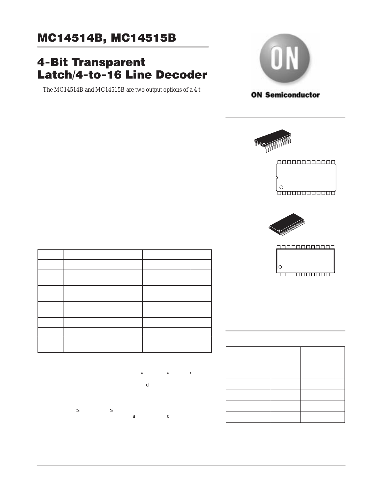
PIN ASSIGNMENT
1
ST
2
D1
3
D2
4
S7
5
S6 S10
S5
6
7
S4
8
S3
9
S1
10
S2
S0
11
V
12
SS
24
V
DD
23
INH
22
D4
21
D3
20
S11
19
S8
18
17
S9
16
S14
15
S15
S12
14
S13
13
DECODE TRUTH TABLE (Strobe = 1)*
Data Inputs
Inhibit D C B A MC14515 = Logic “0”
00000 S0
00001 S1
00010 S2
00011 S3
00100 S4
00101 S5
00110 S6
00111 S7
01000 S8
01001 S9
0 1 0 1 0 S10
01011 S11
0 1 1 0 0 S12
0 1 1 0 1 S13
0 1 1 1 0 S14
0 1 1 1 1 S15
1 X X X X All Outputs = 0, MC14514
X = Don’t Care
*Strobe = 0, Data is latched
Selected Output
MC14514 = Logic “1”
All Outputs = 1, MC14515
BLOCK DIAGRAM
DATA 1
DATA 2
DATA 3
DATA 4
STROBE
INHIBIT
V
DD
V
SS
2
3
TRANSPARENT
21
22
1
23
= PIN 24
= PIN 12
A
B
LATCH
C
D20
http://onsemi.com
2
4 TO 16
DECODER
S0
S1
S2
S3
S4
S5
S6
S7
S8
S9
S10
S11
S12
S13
S14
11
B C D
A
9
A B C D
10
A B C D
8
A B C D
7
A B C D
6
A B C D
5
A B C D
4
A B C D
18
A B C D
17
C D
A B
A
B C D
19
A B C
B C D
A
A B
A
B C D
A B C DS15
D
C D
14
13
16
15
Page 3
MC14514B, MC14515B
V
DD
ELECTRICAL CHARACTERISTICS (Voltages Referenced to V
V
Characteristic Symbol
Output Voltage “0” Level
= VDD or 0
V
in
“1” Level
V
= 0 or V
in
DD
Input Voltage “0” Level
(V
= 4.5 or 0.5 Vdc)
O
= 9.0 or 1.0 Vdc)
(V
O
(V
= 13.5 or 1.5 Vdc)
O
“1” Level
= 0.5 or 4.5 Vdc)
(V
O
(V
= 1.0 or 9.0 Vdc)
O
= 1.5 or 13.5 Vdc)
(V
O
Output Drive Current
(V
= 2.5 Vdc) Source
OH
= 4.6 Vdc)
(V
OH
(V
= 9.5 Vdc)
OH
(V
= 13.5 Vdc)
OH
(VOL = 0.4 Vdc) Sink
(V
= 0.5 Vdc)
OL
(V
= 1.5 Vdc)
OL
Input Current I
Input Capacitance
(V
= 0)
in
Quiescent Current
(Per Package)
Total Supply Current
(4.) (5.)
(Dynamic plus Quiescent,
Per Package)
= 50 pF on all outputs, all
(C
L
V
OL
V
OH
V
V
I
OH
I
OL
in
C
I
DD
I
TL
Vdc
5.0
10
15
5.0
10
15
IL
5.0
10
15
IH
5.0
10
15
5.0
5.0
10
15
5.0
10
15
Min Max Min Typ
—
—
—
4.95
9.95
14.95
—
—
—
3.5
7.0
11
– 1.2
– 0.25
– 0.62
– 1.8
0.64
1.6
4.2
15 — ± 0.1 — ±0.00001 ± 0.1 — ± 1.0 µAdc
in
— — — — 5.0 7.5 — — pF
5.0
10
15
—
—
—
5.0
10
15
)
SS
– 55_C 25_C 125_C
(3.)
Max Min Max
0.05
0.05
0.05
—
—
—
1.5
3.0
4.0
—
—
—
—
—
—
—
—
—
—
5.0
10
20
—
—
—
4.95
9.95
14.95
—
—
—
3.5
7.0
11
– 1.0
– 0.2
– 0.5
– 1.5
0.51
1.3
3.4
—
—
—
0
0
0
5.0
10
15
2.25
4.50
6.75
2.75
5.50
8.25
– 1.7
– 0.36
– 0.9
– 3.5
0.88
2.25
8.8
0.005
0.010
0.015
IT = (1.35 µA/kHz) f + I
IT = (2.70 µA/kHz) f + I
IT = (4.05 µA/kHz) f + I
0.05
0.05
0.05
—
—
—
1.5
3.0
4.0
—
—
—
—
—
—
—
—
—
—
5.0
10
20
DD
DD
DD
—
—
—
4.95
9.95
14.95
—
—
—
3.5
7.0
11
– 0.7
– 0.14
– 0.35
– 1.1
0.36
0.9
2.4
—
—
—
0.05
0.05
0.05
150
300
600
buffers switching)
3. Data labelled “Typ” is not to be used for design purposes but is intended as an indication of the IC’s potential performance.
4. The formulas given are for the typical characteristics only at 25_C.
5. To calculate total supply current at loads other than 50 pF:
I
) = IT(50 pF) + (CL – 50) Vfk
T(CL
where: I
is in µA (per package), CL in pF, V = (VDD – VSS) in volts, f in kHz is input frequency, and k = 0.002.
T
—
—
—
1.5
3.0
4.0
—
—
—
—
—
—
—
—
—
—
Unit
Vdc
Vdc
Vdc
Vdc
mAdc
mAdc
µAdc
µAdc
http://onsemi.com
3
Page 4
MC14514B, MC14515B
SWITCHING CHARACTERISTICS
(6.)
(C
= 50 pF, T
L
= 25_C)
A
All Types
Characteristic Symbol V
Output Rise Time
t
= (3.0 ns/pF) CL + 30 ns
TLH
= (1.5 ns/pF) CL + 15 ns
t
TLH
t
= (1.1 ns/pF) CL + 10 ns
TLH
Output Fall Time
t
= (1.5 ns/pF) CL + 25 ns
THL
= (0.75 ns/pF) CL + 12.5 ns
t
THL
t
= (0.55 ns/pF) CL + 9.5 ns
THL
Propagation Delay Time; Data, Strobe to S
t
, t
PLH
t
PLH
t
PLH
= (1.7 ns/pF) CL + 465 ns
PHL
, t
= (0.86 ns/pF) CL + 192 ns
PHL
, t
= (0.5 ns/pF) CL + 125 ns
PHL
Inhibit Propagation Delay Times
t
, t
PLH
t
PLH
t
PLH
= (1.7 ns/pF) CL + 315 ns
PHL
, t
= (0.66 ns/pF) CL + 117 ns
PHL
, t
= (0.5 ns/pF) CL + 75 ns
PHL
Setup Time
Data to Strobe
Hold Time
Strobe to Data
Strobe Pulse Width t
t
t
t
TLH
t
THL
PLH
t
PHL
PLH
t
PHL
t
WH
DD
5.0
10
15
5.0
10
15
Min Typ
—
—
—
—
—
—
,
5.0
10
15
—
—
—
,
5.0
10
15
su
5.0
10
15
t
h
5.0
10
15
5.0
10
15
—
—
—
250
100
75
– 20
0
10
350
100
75
(7.)
180
90
65
100
50
40
550
225
150
400
150
100
125
50
38
– 100
– 40
– 30
175
50
38
6. The formulas given are for the typical characteristics only at 25_C.
7. Data labelled “Typ” is not to be used for design purposes but is intended as an indication of the IC’s potential performance.
Max
360
180
130
200
100
80
1100
450
300
800
300
200
—
—
—
—
—
—
—
—
—
Unit
ns
ns
ns
ns
ns
ns
ns
For MC14514B
1. For P–channel: Inhibit = V
1. and D1–D4 constitute
1. binary code for “output
1. under test.”
2. For N–channel: Inhibit = V
SS
DD
V
DD
S0
STROBE
INHIBIT
S1
S2
S3
S4
S5
S10
S11
S12
S13
S14
S6
S7
S8
S9
I
D
EXTERNAL
POWER SUPPLY
D1
D2
D3
D4
S15
V
SS
Figure 1. Drain Characteristics T est Circuit
V
DS
For MC14515B
1. For P–channel: Inhibit = V
2. For N–channel: Inhibit = V
2. and D1–D4 constitute binary
2. code for “output
DD
SS
under test.”
http://onsemi.com
4
Page 5

MC14514B, MC14515B
V
V
DD
PROGRAMMABLE
PULSE
GENERATOR
PULSE
GENERATOR
0.01 µF
CERAMIC
C
L
20 ns
V
90%
in
10%
D1
D2
D3
I
D
24
500
µF
V
DD
S0
D4
STROBE
INHIBIT
S15
C
12
V
SS
L
Figure 2. Dynamic Power Dissipation Test Circuit and Waveform
DD
STROBE
INHIBIT
D1
D2
D3
D4
S0
S1
C
L
S15
V
SS
OUTPUT S0
OUTPUT S1
C
L
OUTPUT S15
C
L
INPUT
OUTPUT
t
PLH
10%
t
TLH
t
TLH
90%
50%
20 ns
90%
50%
10%
20 ns
V
DD
V
SS
t
THL
V
DD
V
SS
t
PHL
V
DD
V
SS
t
THL
Figure 3. Switching Time Test Circuit and Waveforms
http://onsemi.com
5
Page 6

MC14514B, MC14515B
11 S0
9S1
10 S2
8S3
7S4
6S5
5S6
4S7
18 S8
17 S9
20 S10
19 S11
14 S12
13 S13
16 S14
15 S15
B C D
A
ABC D
LOGIC DIAGRAM
C D
A BCD
ABCD
A B CD
ABCD
A BCD
ABCD
A B C D
AB
BCD
A
ABCDA
B CD
ABCDA
BCD
ABCD
IN MC14515B ONLY
A
Q
S
DATA 1 2
B
QR
Q
S
DATA 2 3
C
QR
Q
DATA 3 21
D
QRSQ
DATA 4 22
QR
S
STROBE 1
INHIBIT 23
http://onsemi.com
6
Page 7

MC14514B, MC14515B
COMPLEX DATA ROUTING
T wo MC14512 eight–channel data selectors are used here
with the MC14514B four–bit latch/decoder to effect a
complex data routing system. A total of 16 inputs from data
registers are selected and transferred via a 3–state data bus
to a data distributor for rearrangement and entry into 16
output registers. In this way sequential data can be re–routed
or intermixed according to patterns determined by data
select and distribution inputs.
Data is placed into the routing scheme via the eight inputs
on both MC14512 data selectors. One register is assigned to
each input. The signals on A0, A1, and A2 choose one of
eight inputs for transfer out to the 3–state data bus. A fourth
signal, labelled Dis, disables one of the MC14512 selectors,
assuring transfer of data from only one register .
In addition to a choice of input registers, 1 thru 16, the rate
of transfer of the sequential information can also be varied.
That is, if the MC14512 were addressed at a rate that is eight
DATA ROUTING SYSTEM
INPUT
REGISTERS
DATA
TRANSFER
times faster then the shift frequency of the input registers,
the most significant bit (MSB) from each register could be
selected for transfer to the data bus. Therefore, all of the
most significant bits from all of the registers can be
transferred to the data bus before the next most significant
bit is presented for transfer by the input registers.
Information from the 3–state bus is redistributed by the
MC14514B four–bit latch/decoder. Using the four–bit
address, D1 thru D4, the information on the inhibit line can
be transferred to the addressed output line to the desired
output registers, A thru P . This distribution of data bits to the
output registers can be made in many complex patterns. For
example, all of the most significant bits from the input
registers can be routed into output register A, all of the next
most significant bits into register B, etc. In this way
horizontal, vertical, or other methods of data slicing can be
implemented.
3–STATE
DATA BUS
DATA
DISTRIBUTION
OUTPUT
REGISTERS
DATA
SELECT
REGISTER 1
REGISTER 8
REGISTER 9
REGISTER 16
DIS
D0
D1
D2
D3
D4
D5
D6
D7
A0 A1 A2
A0 A1 A2
D0
D1
D2
D3
D4
D5
D6
D7
DIS
Q
MC14512MC14512
Q
D1 D2 D3 D4
STROBE
MC14514B
INHIBIT
S0
S1
S2
S3
S4
S5
S6
S7
S8
S9
S10
S11
S12
S13
S14
S15
REGISTER A
REGISTER P
http://onsemi.com
7
Page 8

1324
B
112
A
N
C
K
H
G
F
D
SEATING
PLANE
MC14514B, MC14515B
P ACKAGE DIMENSIONS
PDIP–24
P SUFFIX
PLASTIC DIP PACKAGE
CASE 709–02
ISSUE C
J
L
M
NOTES:
1. POSITIONAL TOLERANCE OF LEADS (D),
SHALL BE WITHIN 0.25 (0.010) AT MAXIMUM
MATERIAL CONDITION, IN RELATION TO
SEATING PLANE AND EACH OTHER.
2. DIMENSION L TO CENTER OF LEADS WHEN
FORMED PARALLEL.
3. DIMENSION B DOES NOT INCLUDE MOLD
FLASH.
4. CONTROLLING DIMENSION: INCH.
DIM MIN MAX MIN MAX
A 31.37 32.131.235 1.265
B 13.72 14.220.540 0.560
C 3.94 5.080.155 0.200
D 0.36 0.560.014 0.022
F 1.02 1.520.040 0.060
G 2.54 BSC0.100 BSC
H 1.65 2.030.065 0.080
J 0.20 0.380.008 0.015
K 2.92 3.430.115 0.135
L 15.24 BSC0.600 BSC
M 0 15 0 15
____
N 0.51 1.020.020 0.040
MILLIMETERSINCHES
http://onsemi.com
8
Page 9

–T–
SEATING
PLANE
MC14514B, MC14515B
P ACKAGE DIMENSIONS
SOIC–24
DW SUFFIX
PLASTIC SOIC PACKAGE
CASE 751E–04
ISSUE E
–A–
1324
–B– P12X
M
0.010 (0.25) B
1
D24X
0.010 (0.25) B
M
T
12
J
S
A
S
M
F
R
X 45
_
C
M
22X
G
K
NOTES:
1. DIMENSIONING AND TOLERANCING PER ANSI
Y14.5M, 1982.
2. CONTROLLING DIMENSION: MILLIMETER.
3. DIMENSIONS A AND B DO NOT INCLUDE
MOLD PROTRUSION.
4. MAXIMUM MOLD PROTRUSION 0.15 (0.006)
PER SIDE.
5. DIMENSION D DOES NOT INCLUDE DAMBAR
PROTRUSION. ALLOWABLE DAMBAR
PROTRUSION SHALL BE 0.13 (0.005) TOTAL IN
EXCESS OF D DIMENSION AT MAXIMUM
MATERIAL CONDITION.
DIM MIN MAX MIN MAX
A 15.25 15.54 0.601 0.612
B 7.40 7.60 0.292 0.299
C 2.35 2.65 0.093 0.104
D 0.35 0.49 0.014 0.019
F 0.41 0.90 0.016 0.035
G 1.27 BSC 0.050 BSC
J 0.23 0.32 0.009 0.013
K 0.13 0.29 0.005 0.011
M 0 8 0 8
P 10.05 10.55 0.395 0.415
R 0.25 0.75 0.010 0.029
INCHESMILLIMETERS
____
http://onsemi.com
9
Page 10

Notes
MC14514B, MC14515B
http://onsemi.com
10
Page 11

Notes
MC14514B, MC14515B
http://onsemi.com
11
Page 12

MC14514B, MC14515B
ON Semiconductor and are trademarks of Semiconductor Components Industries, LLC (SCILLC). SCILLC reserves the right to make changes
without further notice to any products herein. SCILLC makes no warranty , representation or guarantee regarding the suitability of its products for any particular
purpose, nor does SCILLC assume any liability arising out of the application or use of any product or circuit, and specifically disclaims any and all liability ,
including without limitation special, consequential or incidental damages. “Typical” parameters which may be provided in SCILLC data sheets and/or
specifications can and do vary in different applications and actual performance may vary over time. All operating parameters, including “Typicals” must be
validated for each customer application by customer’s technical experts. SCILLC does not convey any license under its patent rights nor the rights of others.
SCILLC products are not designed, intended, or authorized for use as components in systems intended for surgical implant into the body, or other applications
intended to support or sustain life, or for any other application in which the failure of the SCILLC product could create a situation where personal injury or
death may occur. Should Buyer purchase or use SCILLC products for any such unintended or unauthorized application, Buyer shall indemnify and hold
SCILLC and its officers, employees, subsidiaries, affiliates, and distributors harmless against all claims, costs, damages, and expenses, and reasonable
attorney fees arising out of, directly or indirectly , any claim of personal injury or death associated with such unintended or unauthorized use, even if such claim
alleges that SCILLC was negligent regarding the design or manufacture of the part. SCILLC is an Equal Opportunity/Affirmative Action Employer .
PUBLICATION ORDERING INFORMATION
NORTH AMERICA Literature Fulfillment:
Literature Distribution Center for ON Semiconductor
P.O. Box 5163, Denver, Colorado 80217 USA
Phone: 303–675–2175 or 800–344–3860 Toll Free USA/Canada
Fax: 303–675–2176 or 800–344–3867 Toll Free USA/Canada
Email: ONlit@hibbertco.com
Fax Response Line: 303–675–2167 or 800–344–3810 T oll Free USA/Canada
N. American Technical Support: 800–282–9855 Toll Free USA/Canada
EUROPE: LDC for ON Semiconductor – European Support
German Phone: (+1) 303–308–7140 (M–F 1:00pm to 5:00pm Munich Time)
Email: ONlit–german@hibbertco.com
French Phone: (+1) 303–308–7141 (M–F 1:00pm to 5:00pm Toulouse T ime)
Email: ONlit–french@hibbertco.com
English Phone: (+1) 303–308–7142 (M–F 12:00pm to 5:00pm UK Time)
Email: ONlit@hibbertco.com
EUROPEAN TOLL–FREE ACCESS*: 00–800–4422–3781
*Available from Germany, France, Italy, England, Ireland
CENTRAL/SOUTH AMERICA:
Spanish Phone: 303–308–7143 (Mon–Fri 8:00am to 5:00pm MST)
Email: ONlit–spanish@hibbertco.com
ASIA/PACIFIC : LDC for ON Semiconductor – Asia Support
Phone: 303–675–2121 (Tue–Fri 9:00am to 1:00pm, Hong Kong Time)
T oll Free from Hong Kong & Singapore:
001–800–4422–3781
Email: ONlit–asia@hibbertco.com
JAPAN: ON Semiconductor, Japan Customer Focus Center
4–32–1 Nishi–Gotanda, Shinagawa–ku, T okyo, Japan 141–8549
Phone: 81–3–5740–2745
Email: r14525@onsemi.com
ON Semiconductor Website: http://onsemi.com
For additional information, please contact your local
Sales Representative.
http://onsemi.com
12
MC14514B/D
 Loading...