

Datasheet MC14515BCP, MC14515BCL, MC14514BCP, MC14514BDW, MC14515BDW Datasheet (Motorola)
...Page 1
MOTOROLA CMOS LOGIC DATA
385
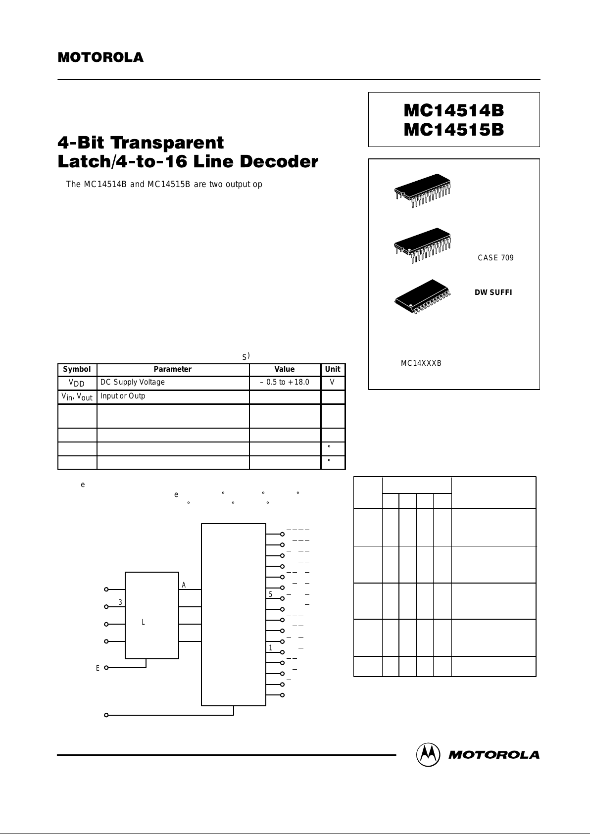
MC14514B MC14515B
The MC14514B and MC14515B are two output options of a 4 to 16 line
decoder with latched inputs. The MC14514B (output active high option)
presents a logical “1” at the selected output, whereas the MC14515B (output
active low option) presents a logical “0” at the selected output. The latches
are R–S type flip–flops which hold the last input data presented prior to the
strobe transition from “1” to “0”. These high and low options of a 4–bit latch/4
to 1 6 line decoder a re constructed with N–channel and P –channel
enhancement mode devices in a single monolithic structure. The latches are
R–S type flip–flops and data is admitted upon a signal incident at the strobe
input, decoded, and presented at the output.
These complementary circuits find primary use in decoding applications
where low power dissipation and/or high noise immunity is desired.
• Supply Voltage Range = 3.0 Vdc to 18 Vdc
• Capable of Driving Two Low–power TTL Loads or One Low–power
Schottky TTL Load Over the Rated Temperature Range
MAXIMUM RATINGS* (Voltages Referenced to V
SS
)
Symbol
Parameter Value Unit
V
DD
DC Supply Voltage – 0.5 to + 18.0 V
Vin, V
out
Input or Output Voltage (DC or Transient) 0.5 to VDD + 0.5 V
Iin, I
out
Input or Output Current (DC or Transient),
per Pin
± 10 mA
P
D
Power Dissipation, per Package† 500 mW
T
stg
Storage Temperature – 65 to + 150
_
C
T
L
Lead Temperature (8–Second Soldering) 260
_
C
*Maximum Ratings are those values beyond which damage to the device may occur.
†Temperature Derating:
Plastic “P and D/DW” Packages: – 7.0 mW/_C From 65_C To 125_C
Ceramic “L” Packages: – 12 mW/_C From 100_C To 125_C
BLOCK DIAGRAM
VDD = PIN 24
VSS = PIN 12
4 TO 16
DECODER
TRANSPARENT
LATCH
STROBE
INHIBIT
2
3
1
21
22
23
DATA 1
DATA 2
DATA 3
DATA 4
A
B
C
D 20
17
18
4
5
6
7
8
10
9
11
19
16
13
14
15
A
B C D
A B C D
A B C D
A B C D
A B C D
A B C D
A B C D
A B C D
A B C D
A B
C D
A
B C D
A B C
D
A B C D
A B
C D
A B C D
A B C DS15
S14
S13
S12
S11
S10
S9
S8
S7
S6
S5
S4
S3
S2
S1
S0
Data Inputs
Selected Output
MC14514 = Logic “1”
Inhibit D C B A MC14515 = Logic “0”
0 0 0 0 0 S0
0 0 0 0 1 S1
0 0 0 1 0 S2
0 0 0 1 1 S3
0 0 1 0 0 S4
0 0 1 0 1 S5
0 0 1 1 0 S6
0 0 1 1 1 S7
0 1 0 0 0 S8
0 1 0 0 1 S9
0 1 0 1 0 S10
0 1 0 1 1 S11
0 1 1 0 0 S12
0 1 1 0 1 S13
0 1 1 1 0 S14
0 1 1 1 1 S15
1 X X X X All Outputs = 0, MC14514
All Outputs = 1, MC14515
DECODE TRUTH TABLE (Strobe = 1)*
X = Don’t Care
*Strobe = 0, Data is latched
SEMICONDUCTOR TECHNICAL DATA
Motorola, Inc. 1995
REV 3
1/94
L SUFFIX
CERAMIC
CASE 623
ORDERING INFORMATION
MC14XXXBCP Plastic
MC14XXXBCL Ceramic
MC14XXXBDW SOIC
TA = – 55° to 125°C for all packages.
P SUFFIX
PLASTIC
CASE 709
DW SUFFIX
SOIC
CASE 751E
Page 2
MOTOROLA CMOS LOGIC DATAMC14514B MC14515B
386
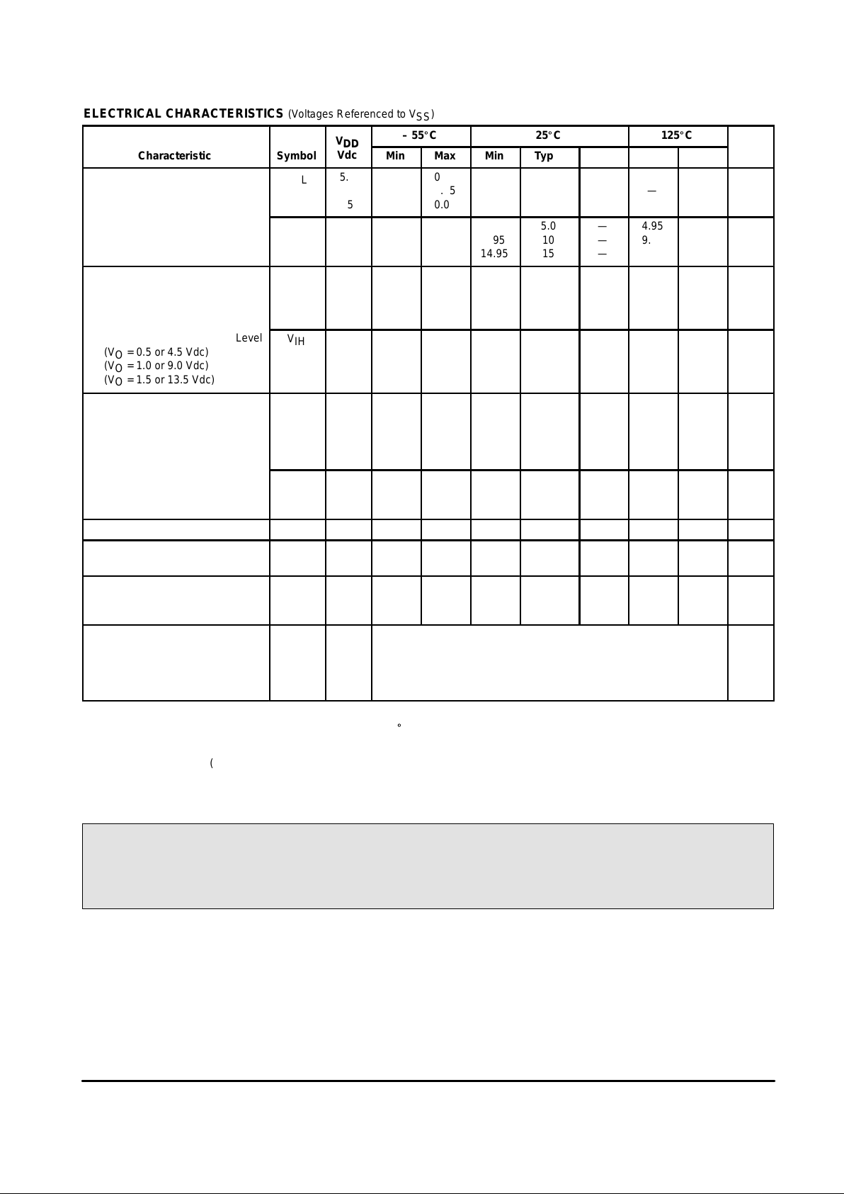
ELECTRICAL CHARACTERISTICS (Voltages Referenced to V
SS
)
V
– 55_C 25_C 125_C
Characteristic
Symbol
V
DD
Vdc
Min Max Min Typ # Max Min Max
Unit
Output Voltage
“0” Level
Vin = VDD or 0
V
OL
5.0
10
15
—
—
—
0.05
0.05
0.05
—
—
—
0
0
0
0.05
0.05
0.05
—
—
—
0.05
0.05
0.05
Vdc
“1” Level
Vin = 0 or V
DD
V
OH
5.0
10
15
4.95
9.95
14.95
—
—
—
4.95
9.95
14.95
5.0
10
15
—
—
—
4.95
9.95
14.95
—
—
—
Vdc
Input Voltage
“0” Level
(VO = 4.5 or 0.5 Vdc)
(VO = 9.0 or 1.0 Vdc)
(VO = 13.5 or 1.5 Vdc)
V
IL
5.0
10
15
—
—
—
1.5
3.0
4.0
—
—
—
2.25
4.50
6.75
1.5
3.0
4.0
—
—
—
1.5
3.0
4.0
Vdc
“1” Level
(VO = 0.5 or 4.5 Vdc)
(VO = 1.0 or 9.0 Vdc)
(VO = 1.5 or 13.5 Vdc)
V
IH
5.0
10
15
3.5
7.0
11
—
—
—
3.5
7.0
11
2.75
5.50
8.25
—
—
—
3.5
7.0
11
—
—
—
Vdc
Output Drive Current
(VOH = 2.5 Vdc) Source
(VOH = 4.6 Vdc)
(VOH = 9.5 Vdc)
(VOH = 13.5 Vdc)
I
OH
5.0
5.0
10
15
– 1.2
– 0.25
– 0.62
– 1.8
—
—
—
—
– 1.0
– 0.2
– 0.5
– 1.5
– 1.7
– 0.36
– 0.9
– 3.5
—
—
—
—
– 0.7
– 0.14
– 0.35
– 1.1
—
—
—
—
mAdc
(VOL = 0.4 Vdc) Sink
(VOL = 0.5 Vdc)
(VOL = 1.5 Vdc)
I
OL
5.0
10
15
0.64
1.6
4.2
—
—
—
0.51
1.3
3.4
0.88
2.25
8.8
—
—
—
0.36
0.9
2.4
—
—
—
mAdc
Input Current I
in
15 — ± 0.1 — ±0.00001 ± 0.1 — ± 1.0 µAdc
Input Capacitance
(Vin = 0)
C
in
— — — — 5.0 7.5 — — pF
Quiescent Current
(Per Package)
I
DD
5.0
10
15
—
—
—
5.0
10
20
—
—
—
0.005
0.010
0.015
5.0
10
20
—
—
—
150
300
600
µAdc
Total Supply Current**†
(Dynamic plus Quiescent,
Per Package)
(CL = 50 pF on all outputs, all
buffers switching)
I
TL
5.0
10
15
IT = (1.35 µA/kHz) f + I
DD
IT = (2.70 µA/kHz) f + I
DD
IT = (4.05 µA/kHz) f + I
DD
µAdc
#Data labelled “Typ” is not to be used for design purposes but is intended as an indication of the IC’s potential performance.
**āThe formulas given are for the typical characteristics only at 25_C.
†To calculate total supply current at loads other than 50 pF:
IT(CL) = IT(50 pF) + (CL – 50) Vfk
where: IT is in µA (per package), CL in pF, V = (VDD – VSS) in volts, f in kHz is input frequency, and k = 0.002.
This device contains protection circuitry to guard against damage due to high static voltages or electric fields. However,
precautions must be taken to avoid applications of any voltage higher than maximum rated voltages to this high-impedance
circuit. For proper operation, Vin and V
out
should be constrained to the range VSS ≤ (Vin or V
out
) ≤ VDD.
Unused inputs must always be tied to an appropriate logic voltage level (e.g., either VSS or VDD). Unused outputs must
be left open.
Page 3
MOTOROLA CMOS LOGIC DATA
387
MC14514B MC14515B
SWITCHING CHARACTERISTICS* (C
L
= 50 pF, TA = 25_C)
All Types
Characteristic
Symbol
V
DD
Min Typ # Max
Unit
Output Rise Time
t
TLH
= (3.0 ns/pF) CL + 30 ns
t
TLH
= (1.5 ns/pF) CL + 15 ns
t
TLH
= (1.1 ns/pF) CL + 10 ns
t
TLH
5.0
10
15
—
—
—
180
90
65
360
180
130
ns
Output Fall Time
t
THL
= (1.5 ns/pF) CL + 25 ns
t
THL
= (0.75 ns/pF) CL + 12.5 ns
t
THL
= (0.55 ns/pF) CL + 9.5 ns
t
THL
5.0
10
15
—
—
—
100
50
40
200
100
80
ns
Propagation Delay Time; Data, Strobe to S
t
PLH
, t
PHL
= (1.7 ns/pF) CL + 465 ns
t
PLH
, t
PHL
= (0.86 ns/pF) CL + 192 ns
t
PLH
, t
PHL
= (0.5 ns/pF) CL + 125 ns
t
PLH
,
t
PHL
5.0
10
15
—
—
—
550
225
150
1100
450
300
ns
Inhibit Propagation Delay Times
t
PLH
, t
PHL
= (1.7 ns/pF) CL + 315 ns
t
PLH
, t
PHL
= (0.66 ns/pF) CL + 117 ns
t
PLH
, t
PHL
= (0.5 ns/pF) CL + 75 ns
t
PLH
,
t
PHL
5.0
10
15
—
—
—
400
150
100
800
300
200
ns
Setup Time
Data to Strobe
t
su
5.0
10
15
250
100
75
125
50
38
—
—
—
ns
Hold Time
Strobe to Data
t
h
5.0
10
15
– 20
0
10
– 100
– 40
– 30
—
—
—
ns
Strobe Pulse Width t
WH
5.0
10
15
350
100
75
175
50
38
—
—
—
ns
*The formulas given are for the typical characteristics only at 25_C.
#Data labelled “Typ” is not to be used for design purposes but is intended as an indication of the IC’s potential performance.
Figure 1. Drain Characteristics Test Circuit
EXTERNAL
POWER SUPPLY
V
SS
STROBE
INHIBIT
D1
D2
D3
D4
V
DD
V
DS
I
D
For MC14515B
1. For P–channel: Inhibit = V
DD
2. For N–channel: Inhibit = V
SS
2. and D1–D4 constitute binary
2. code for “output under test.”
For MC14514B
1. For P–channel: Inhibit = V
SS
1. and D1–D4 constitute
1. binary code for “output
1. under test.”
2. For N–channel: Inhibit = V
DD
S15
S14
S13
S12
S11
S10
S9
S8
S7
S6
S5
S4
S3
S2
S1
S0
Page 4

MOTOROLA CMOS LOGIC DATAMC14514B MC14515B
388
Figure 2. Dynamic Power Dissipation Test Circuit and Waveform
PULSE
GENERATOR
C
L
C
L
V
DD
V
DD
V
SS
S0
S15
12
24
I
D
0.01
µ
F
CERAMIC
500
µ
F
V
DD
V
SS
V
in
20 ns
20 ns
90%
10%
STROBE
D1
D2
D3
D4
INHIBIT
Figure 3. Switching Time Test Circuit and Waveforms
PROGRAMMABLE
PULSE
GENERATOR
V
DD
STROBE
INHIBIT
D1
D2
D3
D4
C
L
V
DD
V
SS
V
DD
V
SS
S0
S1
S15
V
SS
C
L
C
L
INPUT
OUTPUT
t
TLH
t
TLH
t
THL
t
THL
t
PHL
t
PLH
20 ns
OUTPUT S0
OUTPUT S1
OUTPUT S15
90%
50%
10%
90%
50%
10%
S5
S7
D2
D1
ST
S3
S4
S6 S10
D3
D4
INH
V
DD
S15
S14
S9
5
4
3
2
1
10
9
8
7
6
14
15
16
17
18
19
20
13
11
12
21
22
23
24
S13
S12
S8
S11
S0
V
SS
S2
S1
PIN ASSIGNMENT
Page 5

MOTOROLA CMOS LOGIC DATA
389
MC14514B MC14515B
LOGIC DIAGRAM
DATA 1 2
DATA 2 3
DATA 3 21
DATA 4 22
STROBE 1
INHIBIT 23
Q
QR
S
Q
QRSQ
QRSQ
QR
S
A
B
C
D
IN MC14515B ONLY
A
B C D
11 S0
9 S1
10 S2
8 S3
7 S4
6 S5
5 S6
4 S7
18 S8
17 S9
20 S10
19 S11
14 S12
13 S13
16 S14
15 S15
A B C D
A B C D
A B C D
A B C D
A B C D
A B C D
A B C D
A B C D
A B
C D
A
B C D
A B CDA
B C D
A B
C D
A B C D
A B C D
Page 6

MOTOROLA CMOS LOGIC DATAMC14514B MC14515B
390
COMPLEX DATA ROUTING
Two MC14512 eight–channel data selectors are used here
with the MC14514B four–bit latch/decoder to effect a complex data routing system. A total of 16 inputs from data registers are selected and transferred via a 3–state data bus to a
data distributor for rearrangement and entry into 16 output
registers. In this way sequential data can be re–routed or
intermixed according to patterns determined by data select
and distribution inputs.
Data is placed into the routing scheme via the eight inputs
on both MC14512 data selectors. One register is assigned to
each input. The signals on A0, A1, and A2 choose one of
eight inputs for transfer out to the 3–state data bus. A fourth
signal, labelled Dis, disables one of the MC14512 selectors,
assuring transfer of data from only one register.
In addition to a choice of input registers, 1 thru 16, the rate
of transfer of the sequential information can also be varied.
That is, if the MC14512 were addressed at a rate that is eight
times faster then the shift frequency of the input registers, the
most significant bit (MSB) from each register could be selected for transfer to the data bus. Therefore, all of the most
significant bits from all of the registers can be transferred to
the data bus before the next most significant bit is presented
for transfer by the input registers.
Information from the 3–state bus is redistributed by the
MC14514B four–bit latch/decoder. Using the four–bit address, D1 thru D4, the information on the inhibit line can be
transferred to the addressed output line to the desired output
registers, A thru P. This distribution of data bits to the output
registers can be made in many complex patterns. For example, all of the most significant bits from the input registers can
be routed into output register A, all of the next most significant bits into register B, etc. In this way horizontal, vertical, or
other methods of data slicing can be implemented.
DATA ROUTING SYSTEM
INPUT
REGISTERS
DATA
TRANSFER
DATA
DISTRIBUTION
OUTPUT
REGISTERS
3–STATE
DATA BUS
REGISTER A
REGISTER P
REGISTER 1
REGISTER 8
REGISTER 9
REGISTER 16
DATA
SELECT
STROBE
INHIBIT
DIS
DIS
Q
Q
D1 D2 D3 D4
A0 A1 A2
A0 A1 A2
MC14514B
MC14512MC14512
D0
D1
D2
D3
D4
D5
D6
D7
D0
D1
D2
D3
D4
D5
D6
D7
S15
S14
S13
S12
S11
S10
S9
S8
S7
S6
S5
S4
S3
S2
S1
S0
Page 7

MOTOROLA CMOS LOGIC DATA
391
MC14514B MC14515B
OUTLINE DIMENSIONS
P SUFFIX
PLASTIC DIP PACKAGE
CASE 709–02
ISSUE C
L SUFFIX
CERAMIC DIP PACKAGE
CASE 623–05
ISSUE M
NOTES:
1. POSITIONAL TOLERANCE OF LEADS (D),
SHALL BE WITHIN 0.25 (0.010) AT MAXIMUM
MATERIAL CONDITION, IN RELATION TO
SEATING PLANE AND EACH OTHER.
2. DIMENSION L TO CENTER OF LEADS WHEN
FORMED PARALLEL.
3. DIMENSION B DOES NOT INCLUDE MOLD
FLASH.
DIM MIN MAX MIN MAX
INCHESMILLIMETERS
A 31.37 32.13 1.235 1.265
B 13.72 14.22 0.540 0.560
C 3.94 5.08 0.155 0.200
D 0.36 0.56 0.014 0.022
F 1.02 1.52 0.040 0.060
G 2.54 BSC 0.100 BSC
H 1.65 2.03 0.065 0.080
J 0.20 0.38 0.008 0.015
K 2.92 3.43 0.115 0.135
L 15.24 BSC 0.600 BSC
M 0 15 0 15
N 0.51 1.02 0.020 0.040
_ _ _ _
1 12
1324
B
H
A
F
D
G
K
SEATING
PLANE
N
C
M
J
L
NOTES:
1. DIMENSION L TO CENTER OF LEADS WHEN
FORMED PARALLEL.
2. LEADS WITHIN 0.13 (0.005) RADIUS OF TRUE
POSITION AT SEATING PLANE AT MAXIMUM
MATERIAL CONDITION (WHEN FORMED
PARALLEL).
1 12
24 13
B
A
SEATING
PLANE
F
D
G
K
N
C
M
J
L
DIM MIN MAX MIN MAX
INCHESMILLIMETERS
A 31.24 32.77 1.230 1.290
B 12.70 15.49 0.500 0.610
C 4.06 5.59 0.160 0.220
D 0.41 0.51 0.016 0.020
F 1.27 1.52 0.050 0.060
G 2.54 BSC 0.100 BSC
J 0.20 0.30 0.008 0.012
K 3.18 4.06 0.125 0.160
L 15.24 BSC 0.600 BSC
M 0 15 0 15
N 0.51 1.27 0.020 0.050
_ _ _ _
Page 8

MOTOROLA CMOS LOGIC DATAMC14514B MC14515B
392
OUTLINE DIMENSIONS
DW SUFFIX
PLASTIC SOIC PACKAGE
CASE 751E–04
ISSUE E
NOTES:
1. DIMENSIONING AND TOLERANCING PER ANSI
Y14.5M, 1982.
2. CONTROLLING DIMENSION: MILLIMETER.
3. DIMENSIONS A AND B DO NOT INCLUDE
MOLD PROTRUSION.
4. MAXIMUM MOLD PROTRUSION 0.15 (0.006)
PER SIDE.
5. DIMENSION D DOES NOT INCLUDE DAMBAR
PROTRUSION. ALLOWABLE DAMBAR
PROTRUSION SHALL BE 0.13 (0.005) TOTAL IN
EXCESS OF D DIMENSION AT MAXIMUM
MATERIAL CONDITION.
–A–
–B– P12X
D24X
12
1324
1
M
0.010 (0.25) B
M
S
A
M
0.010 (0.25) B
S
T
–T–
G
22X
SEATING
PLANE
K
C
R
X 45
_
M
F
J
DIM MIN MAX MIN MAX
INCHESMILLIMETERS
A 15.25 15.54 0.601 0.612
B 7.40 7.60 0.292 0.299
C 2.35 2.65 0.093 0.104
D 0.35 0.49 0.014 0.019
F 0.41 0.90 0.016 0.035
G 1.27 BSC 0.050 BSC
J 0.23 0.32 0.009 0.013
K 0.13 0.29 0.005 0.011
M 0 8 0 8
P 10.05 10.55 0.395 0.415
R 0.25 0.75 0.010 0.029
____
How to reach us:
USA/EUROPE/Locations Not Listed: Motorola Literature Distribution; JAPAN: Nippon Motorola Ltd.; Tatsumi–SPD–JLDC, 6F Seibu–Butsuryu–Center,
P.O. Box 20912; Phoenix, Arizona 85036. 1–800–441–2447 or 602–303–5454 3–14–2 Tatsumi Koto–Ku, Tokyo 135, Japan. 03–81–3521–8315
MFAX: RMFAX0@email.sps.mot.com – TOUCHTONE 602–244–6609 ASIA/PACIFIC: Motorola Semiconductors H.K. Ltd.; 8B Tai Ping Industrial Park,
INTERNET: http://Design–NET.com 51 Ting Kok Road, Tai Po, N.T., Hong Kong. 852–26629298
Motorola reserves the right to make changes without further notice to any products herein. Motorola makes no warranty , representation or guarantee regarding
the suitability of its products for any particular purpose, nor does Motorola assume any liability arising out of the application or use of any product or circuit,
and specifically disclaims any and all liability, including without limitation consequential or incidental damages. “Typical” parameters which may be provided
in Motorola data sheets and/or specifications can and do vary in different applications and actual performance may vary over time. All operating parameters,
including “Typicals” must be validated for each customer application by customer’s technical experts. Motorola does not convey any license under its patent
rights nor the rights of others. Motorola products are not designed, intended, or authorized for use as components in systems intended for surgical implant
into the body, or other applications intended to support or sustain life, or for any other application in which the failure of the Motorola product could create a
situation where personal injury or death may occur. Should Buyer purchase or use Motorola products for any such unintended or unauthorized application,
Buyer shall indemnify and hold Motorola and its officers, employees, subsidiaries, affiliates, and distributors harmless against all claims, costs, damages, and
expenses, and reasonable attorney fees arising out of, directly or indirectly, any claim of personal injury or death associated with such unintended or
unauthorized use, even if such claim alleges that Motorola was negligent regarding the design or manufacture of the part. Motorola and are registered
trademarks of Motorola, Inc. Motorola, Inc. is an Equal Opportunity/Affirmative Action Employer .
MC14514B/D
*MC14514B/D*
◊
 Loading...