

Page 1
MOTOROLA CMOS LOGIC DATAMC14508B
344
The MC14508B dual 4–bit latch is constructed with MOS P–channel and
N–channel enhancement mode devices in a single monolithic structure. The
part consists of two identical, independent 4–bit latches with separate Strobe
(ST) and Master Reset (MR) controls. Separate Disable inputs force the
outputs to a high impedance state and allow the devices to be used in time
sharing bus line applications.
These complementary MOS latches find primary use in buffer storage,
holding register, o r general digital logic functions where low power
dissipation and/or high noise immunity is desired.
• 3–State Output
• Supply Voltage Range = 3.0 Vdc to 18 Vdc
• Capable–of Driving Two Low–power TTL Loads or One Low–power
Schottky TTL Load over the Rated Temperature Range
MAXIMUM RATINGS* (Voltages Referenced to V
SS
)
Symbol
Parameter Value Unit
V
DD
DC Supply Voltage – 0.5 to + 18.0 V
Vin, V
out
Input or Output Voltage (DC or Transient) – 0.5 to VDD + 0.5 V
Iin, I
out
Input or Output Current (DC or Transient),
per Pin
± 10 mA
P
D
Power Dissipation, per Package† 500 mW
T
stg
Storage Temperature – 65 to + 150
_
C
T
L
Lead Temperature (8–Second Soldering) 260
_
C
*Maximum Ratings are those values beyond which damage to the device may occur.
†Temperature Derating:
Plastic “P and D/DW” Packages: – 7.0 mW/_C From 65_C To 125_C
Ceramic “L” Packages: – 12 mW/_C From 100_C To 125_C
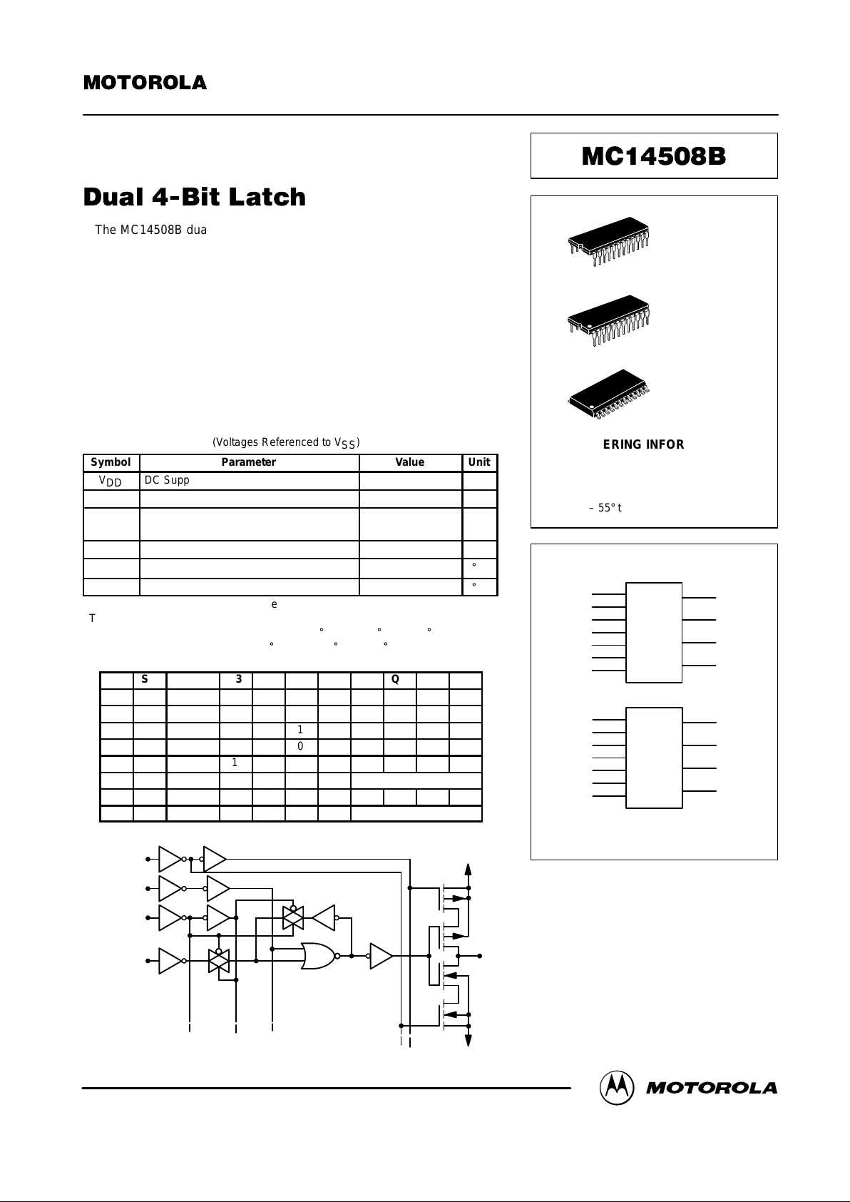
TRUTH TABLE
MR ST Disable D3 D2 D1 D0 Q3 Q2 Q1 Q0
0 1 0 0 0 0 0 0 0 0 0
0 1 0 0 0 0 1 0 0 0 1
0 1 0 0 0 1 0 0 0 1 0
0 1 0 0 1 0 0 0 1 0 0
0 1 0 1 0 0 0 1 0 0 0
0 0 0 X X X X Latched
1 X 0 X X X X 0 0 0 0
X X 1 X X X X High Impedance
X = Don’t Care
CIRCUIT DIAGRAM
DIS
MR
ST
D
n
(TO OTHER THREE LATCHES)
V
DD
Q
n
V
SS
SEMICONDUCTOR TECHNICAL DATA
Motorola, Inc. 1995
REV 3
1/94
L SUFFIX
CERAMIC
CASE 623
ORDERING INFORMATION
MC14XXXBCP Plastic
MC14XXXBCL Ceramic
MC14XXXBDW SOIC
TA = – 55° to 125°C for all packages.
P SUFFIX
PLASTIC
CASE 709
DW SUFFIX
SOIC
CASE 751E
BLOCK DIAGRAM
22
20
18
16
15
14
13
10
8
6
4
3
2
1
23
21
19
17
11
9
7
5
MR
ST
DIS
D0
D1
D2
D3
MR
ST
DIS
D0
D1
D2
D3
Q0
Q1
Q2
Q3
Q0
Q1
Q2
Q3
VDD = PIN 24
VSS = PIN 12
Page 2
MOTOROLA CMOS LOGIC DATA
345
MC14508B
ELECTRICAL CHARACTERISTICS (Voltages Referenced to V
SS
)
V
– 55_C 25_C 125_C
Characteristic
Symbol
V
DD
Vdc
Min Max Min Typ # Max Min Max
Unit
Output Voltage
“0” Level
Vin = VDD or 0
V
OL
5.0
10
15
—
—
—
0.05
0.05
0.05
—
—
—
0
0
0
0.05
0.05
0.05
—
—
—
0.05
0.05
0.05
Vdc
“1” Level
Vin = 0 or V
DD
V
OH
5.0
10
15
4.95
9.95
14.95
—
—
—
4.95
9.95
14.95
5.0
10
15
—
—
—
4.95
9.95
14.95
—
—
—
Vdc
Input Voltage
“0” Level
(VO = 4.5 or 0.5 Vdc)
(VO = 9.0 or 1.0 Vdc)
(VO = 13.5 or 1.5 Vdc)
V
IL
5.0
10
15
—
—
—
1.5
3.0
4.0
—
—
—
2.25
4.50
6.75
1.5
3.0
4.0
—
—
—
1.5
3.0
4.0
Vdc
“1” Level
(VO = 0.5 or 4.5 Vdc)
(VO = 1.0 or 9.0 Vdc)
(VO = 1.5 or 13.5 Vdc)
V
IH
5.0
10
15
3.5
7.0
11
—
—
—
3.5
7.0
11
2.75
5.50
8.25
—
—
—
3.5
7.0
11
—
—
—
Vdc
Output Drive Current
(VOH = 2.5 Vdc) Source
(VOH = 4.6 Vdc)
(VOH = 9.5 Vdc)
(VOH = 13.5 Vdc)
I
OH
5.0
5.0
10
15
– 3.0
– 0.64
– 1.6
– 4.2
—
—
—
—
– 2.4
– 0.51
– 1.3
– 3.4
– 4.2
– 0.88
– 2.25
– 8.8
—
—
—
—
– 1.7
– 0.36
– 0.9
– 2.4
—
—
—
—
mAdc
(VOL = 0.4 Vdc) Sink
(VOL = 0.5 Vdc)
(VOL = 1.5 Vdc)
I
OL
5.0
10
15
0.64
1.6
4.2
—
—
—
0.51
1.3
3.4
0.88
2.25
8.8
—
—
—
0.36
0.9
2.4
—
—
—
mAdc
Input Current I
in
15 — ± 0.1 — ±0.00001 ± 0.1 — ± 1.0 µAdc
Input Capacitance
(Vin = 0)
C
in
— — — — 5.0 7.5 — — pF
Quiescent Current
(Per Package)
I
DD
5.0
10
15
—
—
—
5.0
10
20
—
—
—
0.005
0.010
0.015
5.0
10
20
—
—
—
150
300
600
µAdc
Total Supply Current**†
(Dynamic plus Quiescent,
Per Package)
(CL = 50 pF on all outputs, all
buffers switching)
I
T
5.0
10
15
IT = (1.46 µA/kHz) f + I
DD
IT = (2.91 µA/kHz) f + I
DD
IT = (4.37 µA/kHz) f + I
DD
µAdc
Three–State Leakage Current I
TL
15 — ± 0.1 — ± 0.0001 ± 0.1 — ± 3.0 µAdc
#Data labelled “Typ” is not to be used for design purposes but is intended as an indication of the IC’s potential performance.
**āThe formulas given are for the typical characteristics only at 25_C.
†To calculate total supply current at loads other than 50 pF:
IT(CL) = IT(50 pF) + (CL – 50) Vfk
where: IT is in µA (per package), CL in pF, V = (VDD – VSS) in volts, f in kHz is input frequency, and k = 0.008.
This device contains protection circuitry to guard against damage due to high static voltages or electric fields. However,
precautions must be taken to avoid applications of any voltage higher than maximum rated voltages to this high-impedance
circuit. For proper operation, Vin and V
out
should be constrained to the range VSS ≤ (Vin or V
out
) ≤ VDD.
Unused inputs must always be tied to an appropriate logic voltage level (e.g., either VSS or VDD). Unused outputs must
be left open.
Page 3
MOTOROLA CMOS LOGIC DATAMC14508B
346
SWITCHING CHARACTERISTICS* (C
L
= 50 pF, TA = 25_C)
All Types
Characteristic
Symbol
V
DD
Min Typ # Max
Unit
Output Rise and Fall Time
t
TLH
, t
THL
= (1.5 ns/pF) CL + 25 ns
t
TLH
, t
THL
= (0.75 ns/pF) CL + 12.5 ns
t
TLH
, t
THL
= (0.55 ns/pF) CL + 9.5 ns
t
TLH
, t
THL
5.0
10
15
—
—
—
100
50
40
200
100
80
ns
Propagation Delay Time, Dn or MR to Q
t
PLH
, t
PHL
= (1.7 ns/pF) CL + 135 ns
t
PLH
, t
PHL
= (0.66 ns/pF) CL + 57 ns
t
PLH
, t
PHL
= (0.5 ns/pF) CL + 35 ns
t
PLH
, t
PHL
5.0
10
15
—
—
—
220
90
60
440
180
120
ns
Master Reset Pulse Width t
WH(R)
5.0
10
15
200
100
70
100
50
35
—
—
—
ns
Master Reset Removal Time t
rem
5.0
10
15
30
25
20
– 15
0
0
—
—
—
ns
Strobe Pulse Width t
WH(S)
5.0
10
15
140
70
40
70
35
20
—
—
—
ns
Setup Time
Data to Strobe
t
su
5.0
10
15
50
20
10
25
10
5.0
—
—
—
ns
Hold Time
Strobe to Data
t
h
5.0
10
15
50
35
35
20
10
10
—
—
—
ns
3–State Propagation Delay Time
Output “1” to High Impedance
t
PHZ
5.0
10
15
—
—
—
55
35
30
170
100
70
ns
Output “0” to High Impedance t
PLZ
5.0
10
15
—
—
—
75
40
35
170
100
70
High Impedance to “1” Level t
PZH
5.0
10
15
—
—
—
80
35
30
170
100
70
High Impedance to “0” Level t
PZL
5.0
10
15
—
—
—
105
50
35
210
100
70
*The formulas given are for the typical characteristics only at 25_C.
#Data labelled “Typ” is not to be used for design purposes but is intended as an indication of the IC’s potential performance.
PIN ASSIGNMENT
D1
A
D0
A
DIS
A
ST
A
MR
A
D2
A
Q1
A
Q0
A
D2
B
Q2
B
D3
B
Q3
B
V
DD
DIS
B
D0
B
Q0
B
5
4
3
2
1
10
9
8
7
6
14
15
16
17
18
19
20
13
11
12
21
22
23
24
MR
B
ST
B
D1
B
Q1
B
Q3
A
V
SS
D3
A
Q2
A
Page 4
MOTOROLA CMOS LOGIC DATA
347
MC14508B
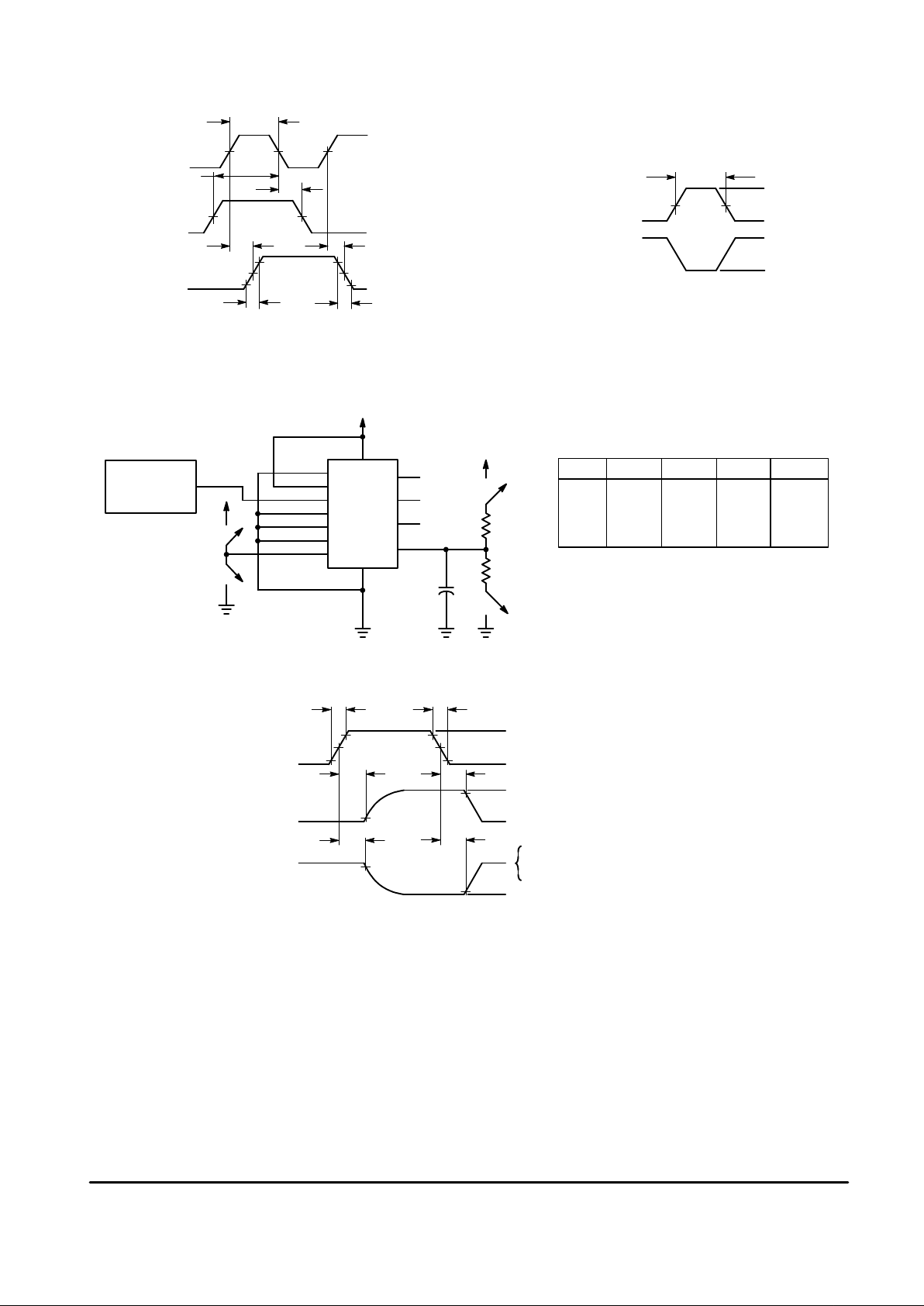
Figure 1. AC Waveforms
STROBE
INPUT
Dn INPUT
Qn OUTPUT
t
TLH
t
THL
t
PHL
t
PLH
50% 50%
t
h
t
su
50%
90%
10%
50%
MASTER RESET
INPUT
Qn OUTPUT
V
DD
V
SS
V
OH
V
OL
50%
t
WH(R)
t
WH(S)
Figure 2. 3–State AC Test Circuit and Waveforms
Test ST1 ST2 ST3 ST4
t
PHZ
Open Close Close Open
t
PLZ
Close Open Open Close
t
PZL
Close Open Open Close
t
PZH
Open Close Close Open
PULSE
GENERATOR
V
DD
ST3
ST4
V
DD
V
DD
ST1
ST2
C
L
1.0 k
1.0 k
V
SS
MR
ST
DISABLE
D0
D1
D2
D3
Q0
Q1
Q2
Q3
20 ns 20 ns
V
DD
V
SS
V
OH
V
OL
t
PZH
t
PZL
t
PLZ
t
PHZ
DISABLE
Q3 OUTPUT
50%
90%
10%
90%
10%
90%
10%
≈
2 V @ VDD = 5 V
≈
6 V @ VDD = 10 V
≈
10 V @ VDD = 15 V
≈
2.5 V @ VDD = 5 V,
10 V, AND 15 V
Page 5

MOTOROLA CMOS LOGIC DATAMC14508B
348
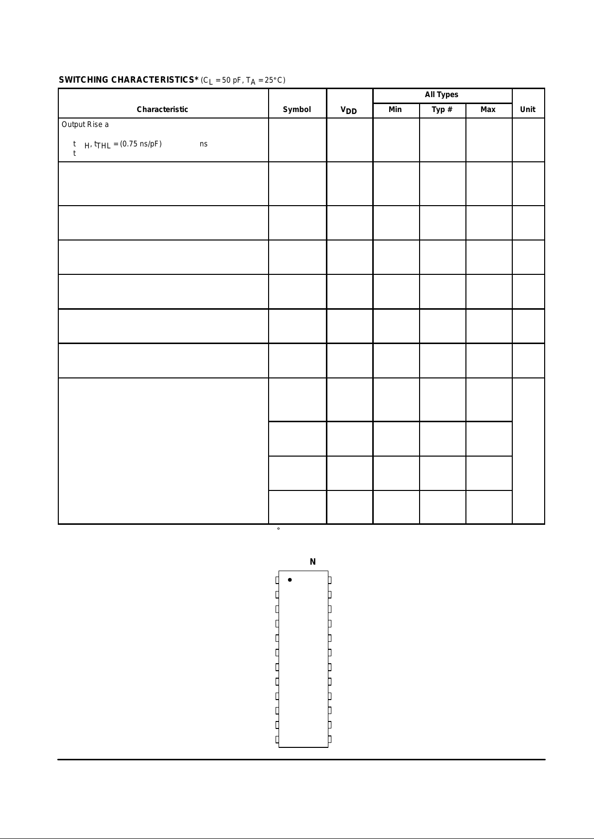
3–STATE MODE OF OPERATION
The MC14508B can be used in bussed systems as shown.
The output terminals of N 4–bit latches can be directly wired
to a bus line, and to one of the 4–bit latches selected. The
selected latch controls the logic state of the bus line and the
remaining (N–1) 4–bit latches are disabled into a high impedance “off” state. The number of latches, N, which may be
connected to a bus line is determined from the output drive
current, IOD, the 3–state or disabled output leakage current,
ITL, and the load current, IL, required to drive the bus line (including fanout to other device inputs) and can be calculated
by the following:
I
TL
N = + 1
IOD – I
L
N must be calculated for both high and low logic states of the
bus line.
SELECTED AS
DRIVING DEVICE
1/2
MC14508B
DISABLED
1/2
MC14508B
DISABLED
1/2
MC14508B
I
OD
I
OD
I
TL
I
TL
I
TL
I
TL
I
L
I
L
BUS LINES
TYPICAL 3–STATE APPLICATIONS
EXAMPLE 1
EXAMPLE 2
DISABLE
DISABLE
STROBE
SERIAL
DATA
CLOCK
RESET
4–LINE DATA BUS
MC14015B
MC
14508B
4–BIT SHIFT
REGISTER
4–BIT SHIFT
REGISTER
QUAD LATCH
(3–STATE)
QUAD LATCH
(3–STATE)
3–STATE
4–BIT LATCH
3–STATE
4–BIT LATCH
3–STATE
4–BIT LATCH
4–LINE DATA BUS
MC
14508B
3–STATE
4–BIT LATCH
4–LINE DATA BUS
MC14519B
A
B
DATA BUS
3–STATE
4–BIT LATCH
14508B
MC
Page 6
MOTOROLA CMOS LOGIC DATA
349
MC14508B
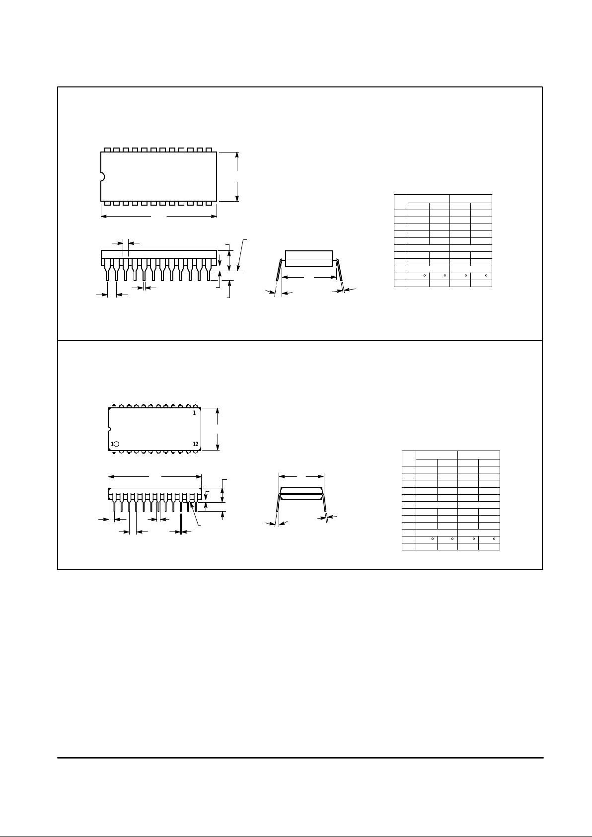
OUTLINE DIMENSIONS
P SUFFIX
PLASTIC DIP PACKAGE
CASE 709–02
ISSUE C
L SUFFIX
CERAMIC DIP PACKAGE
CASE 623–05
ISSUE M
NOTES:
1. POSITIONAL TOLERANCE OF LEADS (D),
SHALL BE WITHIN 0.25 (0.010) AT MAXIMUM
MATERIAL CONDITION, IN RELATION TO
SEATING PLANE AND EACH OTHER.
2. DIMENSION L TO CENTER OF LEADS WHEN
FORMED PARALLEL.
3. DIMENSION B DOES NOT INCLUDE MOLD
FLASH.
DIM MIN MAX MIN MAX
INCHESMILLIMETERS
A 31.37 32.13 1.235 1.265
B 13.72 14.22 0.540 0.560
C 3.94 5.08 0.155 0.200
D 0.36 0.56 0.014 0.022
F 1.02 1.52 0.040 0.060
G 2.54 BSC 0.100 BSC
H 1.65 2.03 0.065 0.080
J 0.20 0.38 0.008 0.015
K 2.92 3.43 0.115 0.135
L 15.24 BSC 0.600 BSC
M 0 15 0 15
N 0.51 1.02 0.020 0.040
_ _ _ _
1 12
1324
B
H
A
F
D
G
K
SEATING
PLANE
N
C
M
J
L
NOTES:
1. DIMENSION L TO CENTER OF LEADS WHEN
FORMED PARALLEL.
2. LEADS WITHIN 0.13 (0.005) RADIUS OF TRUE
POSITION AT SEATING PLANE AT MAXIMUM
MATERIAL CONDITION (WHEN FORMED
PARALLEL).
1 12
24 13
B
A
SEATING
PLANE
F
D
G
K
N
C
M
J
L
DIM MIN MAX MIN MAX
INCHESMILLIMETERS
A 31.24 32.77 1.230 1.290
B 12.70 15.49 0.500 0.610
C 4.06 5.59 0.160 0.220
D 0.41 0.51 0.016 0.020
F 1.27 1.52 0.050 0.060
G 2.54 BSC 0.100 BSC
J 0.20 0.30 0.008 0.012
K 3.18 4.06 0.125 0.160
L 15.24 BSC 0.600 BSC
M 0 15 0 15
N 0.51 1.27 0.020 0.050
_ _ _ _
Page 7

MOTOROLA CMOS LOGIC DATAMC14508B
350
OUTLINE DIMENSIONS
DW SUFFIX
PLASTIC SOIC PACKAGE
CASE 751E–04
ISSUE E
NOTES:
1. DIMENSIONING AND TOLERANCING PER ANSI
Y14.5M, 1982.
2. CONTROLLING DIMENSION: MILLIMETER.
3. DIMENSIONS A AND B DO NOT INCLUDE
MOLD PROTRUSION.
4. MAXIMUM MOLD PROTRUSION 0.15 (0.006)
PER SIDE.
5. DIMENSION D DOES NOT INCLUDE DAMBAR
PROTRUSION. ALLOWABLE DAMBAR
PROTRUSION SHALL BE 0.13 (0.005) TOTAL IN
EXCESS OF D DIMENSION AT MAXIMUM
MATERIAL CONDITION.
–A–
–B– P12X
D24X
12
1324
1
M
0.010 (0.25) B
M
S
A
M
0.010 (0.25) B
S
T
–T–
G
22X
SEATING
PLANE
K
C
R
X 45
_
M
F
J
DIM MIN MAX MIN MAX
INCHESMILLIMETERS
A 15.25 15.54 0.601 0.612
B 7.40 7.60 0.292 0.299
C 2.35 2.65 0.093 0.104
D 0.35 0.49 0.014 0.019
F 0.41 0.90 0.016 0.035
G 1.27 BSC 0.050 BSC
J 0.23 0.32 0.009 0.013
K 0.13 0.29 0.005 0.011
M 0 8 0 8
P 10.05 10.55 0.395 0.415
R 0.25 0.75 0.010 0.029
____
How to reach us:
USA/EUROPE/Locations Not Listed: Motorola Literature Distribution; JAPAN: Nippon Motorola Ltd.; Tatsumi–SPD–JLDC, 6F Seibu–Butsuryu–Center,
P.O. Box 20912; Phoenix, Arizona 85036. 1–800–441–2447 or 602–303–5454 3–14–2 Tatsumi Koto–Ku, Tokyo 135, Japan. 03–81–3521–8315
MFAX: RMFAX0@email.sps.mot.com – TOUCHTONE 602–244–6609 ASIA/PACIFIC: Motorola Semiconductors H.K. Ltd.; 8B Tai Ping Industrial Park,
INTERNET: http://Design–NET.com 51 Ting Kok Road, Tai Po, N.T., Hong Kong. 852–26629298
Motorola reserves the right to make changes without further notice to any products herein. Motorola makes no warranty , representation or guarantee regarding
the suitability of its products for any particular purpose, nor does Motorola assume any liability arising out of the application or use of any product or circuit,
and specifically disclaims any and all liability, including without limitation consequential or incidental damages. “Typical” parameters which may be provided
in Motorola data sheets and/or specifications can and do vary in different applications and actual performance may vary over time. All operating parameters,
including “Typicals” must be validated for each customer application by customer’s technical experts. Motorola does not convey any license under its patent
rights nor the rights of others. Motorola products are not designed, intended, or authorized for use as components in systems intended for surgical implant
into the body, or other applications intended to support or sustain life, or for any other application in which the failure of the Motorola product could create a
situation where personal injury or death may occur. Should Buyer purchase or use Motorola products for any such unintended or unauthorized application,
Buyer shall indemnify and hold Motorola and its officers, employees, subsidiaries, affiliates, and distributors harmless against all claims, costs, damages, and
expenses, and reasonable attorney fees arising out of, directly or indirectly, any claim of personal injury or death associated with such unintended or
unauthorized use, even if such claim alleges that Motorola was negligent regarding the design or manufacture of the part. Motorola and are registered
trademarks of Motorola, Inc. Motorola, Inc. is an Equal Opportunity/Affirmative Action Employer .
MC14508B/D
*MC14508B/D*
◊
 Loading...