

Page 1
MC145076
MOTOROLA
1
Product Preview
CMOS
The MC145076 is a combination re–clocking and smoothing filter designed
especially for the MC145074 Stereo Audio DAC. Its versatility however, allows
it to be used with any single bit–stream data converter to provide output
reconstruction filtering, and to improve performance by restoring pulse shape
integrity. The MC145076 provides a well controlled, filtered output that can be
used directly, or with a current summing operational amplifier.
The MC145076 is intended to be one half of a two–chip solution for serial bit
steam DACs. The analog filtering function of the MC145076 eases the digital
filtering requirements at the input to the digital noise shaping modulator, and
eliminates the need for precision analog output filtering capacitors, resulting in
lower overall system cost. The MC145076 pulse shape restoration frees the
designer from analog pitfalls that can impact performance, thereby lowering the
risk of new product development with a sigma–delta DAC.
• Single–Ended Stereo Outputs Require no Additional Smoothing Filters
• 86 dB S/D, 96 dB S/N with MC145074 @ 192 x OSR Single Ended
• > 100 dB S/(N+D) @ 256 OSR, Differential Mode
• 18.5 MHz Maximum Serial Data Input Rate
• – 80 dB Cross Channel Interference
• 72–Tap FIR with > 40 dB Alias Filtering
• Operating Temperature Range: – 40 to + 85_C
• Buffered Data Clock Output for Ease of Data Generation
• 16–Pin Narrow Body SOIC Package
• Single Supply Operation: + 5 V
TIMING
AND
CONTROL
LOGIC
DIL
5
DIR
6
DIV2
4
TEST
7
X
out
X
in
16
2
V
DDA
1
V
DDD
8
GND
10
GND
15
LEFT 144 SERIAL SHIFT REG.
LEFT CHOP
C (1)
14
IOL
GND
144 TAP HAMMING
WINDOW
COEFFICIENTS
13
9
CLKOUT
RIGHT 144 SERIAL SHIFT REG.
RIGHT CHOP
C (1)
11
IOR
GND
144 TAP HAMMING
WINDOW
COEFFICIENTS
12
C (144)
C (144)
BIAS
3
This document contains information on a product under development. Motorola reserves the right to change or discontinue this product without notice.
Order this document
by MC145076/D
SEMICONDUCTOR TECHNICAL DATA
PIN ASSIGNMENT
D SUFFIX
16–PIN SOG
CASE 751B–05
ORDERING INFORMATION
MC145076D SOG Package
13
14
15
16
9
10
11
125
4
3
2
1
8
7
6
GND
GND
IOL
GND
X
out
CLKOUT
GND
IOR
DIV2
BIAS
X
in
V
DDA
V
DDD
TEST
DIR
DIL
16
1
Motorola, Inc. 1996
REV 1
9/96
Page 2
MC145076
MOTOROLA
2
MAXIMUM RATINGS*
Symbol Parameter Value Unit
V
DD
DC Supply Voltage (Referenced to GND) 6.0 V
V
in
DC Input Voltage
GND
– 0.5 to
VDD + 0.5
V
V
out
DC Output Voltage GND – 0.5 to
VDD + 0.5
V
I
in
DC Input Current, per Pin ± 10 mA
I
out
DC Output Current, per Pin ± 20 mA
IDD,
I
GND
DC Supply Current, VDD and GND Pins ± 60 mA
T
stg
Storage Temperature – 55 to 150 °C
T
L
Lead Temperature, 1 mm from Case for
10 Seconds
260 °C
*Maximum Ratings are those values beyond which damage to the device may occur . Func-
tional operation should be restricted to the Operation Ranges below.
OPERATION RANGES (Applicable to Guaranteed Limits)
Symbol
Parameter Value Unit
V
DD
DC Supply Voltage 4.5 to 5.5 V
V
IOL
,
V
IOR
IOL, IOR Virtual Ground VDD – 2.0 to V
DD
V
T
A
Ambient Operating Temperature – 40 to + 85 °C
DC ELECTRICAL CHARACTERISTICS
(Voltages Referenced to GND, Full Temperature and Voltage Ranges per Operation Ranges Table, unless otherwise indicated)
Symbol
Parameter Guaranteed Limit Unit
V
IH
Minimum High–Level Input Voltage 0.7 x V
DD
V
V
IL
Maximum Low–Level Input Voltage 0.3 x V
DD
V
V
OH
Minimum High–Level Output Voltage IOH = 0.4 mA VDD – 0.3 V
V
OL
Maximum Low–Level Output Voltage IOL = 0.4 mA GND + 0.3 V
I
DD
Maximum Power Supply Current R
bias
= 4640 Ω 40 mA
IOL, I
OR
Left/Right Channel Output Current* 2 ± 20% mA
I
lkg
Input Leakage Current ± 10 µA
*50% Duty Cycle, V
DDA
= 5 V, R
bias
= 4640 Ω
SINGLE ENDED ANALOG CHARACTERISTICS
(Xin = 16.9344 MHz, DIV2 = 0, fin = 990.527 Hz, 20 Bit 2nd Order Modulator Input Data)
Parameter
Test Conditions Min Typ Max Unit
Dynamic Range S/(N+D) @ – 60 dB input, + 60 dB — 96 — dB
S/(N+D) Flat
A–weighted
(– 6 dB) 25 to 75% peak to peak input duty cycle
(– 20 dB)
86
—
90
80*
— dB
Idle Channel Noise CLKOUT/4 digital input data pattern — 105 — dB
60 Hz Power Supply Rejection With 47 µF and 4640 Ω on Bias Pin — 40 — dB
*Noise performance limited by second order digital modulator .
This device contains protection circuitry to
guard against damage due to high static voltages or electric fields. However, precautions
must be taken to avoid applications of any voltage higher than maximum rated voltages to
this high–impedance circuit. For proper operation, Vin and V
out
should be constrained to the
range GND ≤ (Vin or V
out
) ≤ VDD.
Unused inputs must always be tied to an
appropriate logic voltage level (e.g., either
GND or VDD). Unused outputs must be left
open.
Page 3
MC145076
MOTOROLA
3
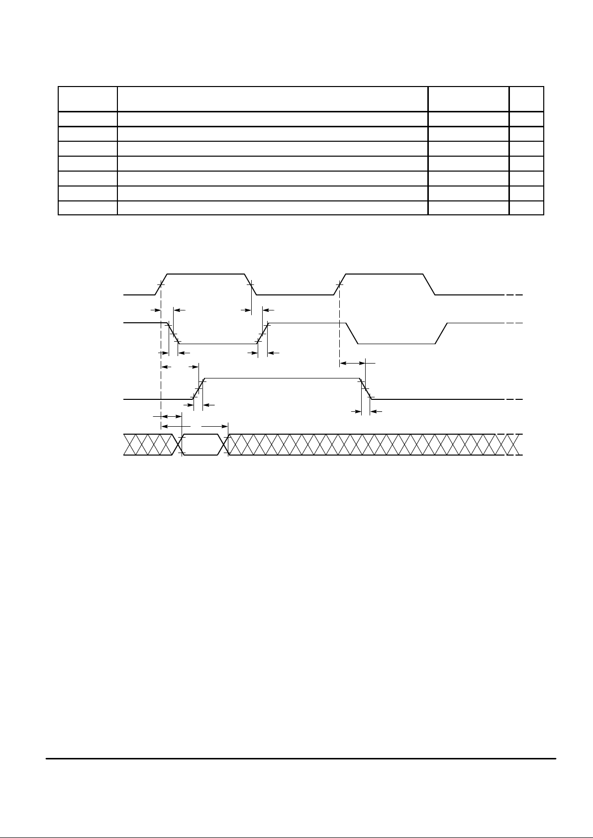
AC ELECTRICAL CHARACTERISTICS (Full Temperature and Voltage Ranges per Operation Ranges Table)
Symbol
Parameter
Guaranteed
Limit
Unit
f Clock Frequency, X
in
37 MHz
t
PLH
, t
PHL
Maximum Propagation Delay, Xin to X
out
5 ns
t
TLH
, t
THL
Maximum Rise/Fall Time, X
out
10 ns
t
PLH
, t
PHL
Maximum Propagation Delay, Xin to CLKOUT 30 ns
t
TLH
, t
THL
Maximum Rise/Fall Time, CLKOUT 10 ns
t
su
Minimum DIR, DIL Setup Time From X
in
5 ns
t
h
Maximum DIR, DIL Hold Time From X
in
20 ns
NOTE: 10 pF load capacitance, Xin rise and fall times set at 2 ns.
TIMING WAVEFORMS
X
in
50%
t
su
t
PHL
X
out
CLKOUT
50%
10%
50%
90%
10%
50%
50% 50%
t
PLH
t
TLH
t
THL
t
TLH
t
THL
t
PLH
t
PHL
t
h
90%
90%
10%
10%
90%
50%
90%
10%
DIR OR DIL
Figure 1.
Page 4

MC145076
MOTOROLA
4
PIN DESCRIPTIONS
Xin, X
out
Oscillator Inverter Input and Output (Pins 2, 16)
If an external clock is used to drive the MC145076, the
clock should be connected to Xin pin. For maximum performance however, it is recommended that these pins be used
in conjunction as a crystal oscillator.
BIAS
Bias Adjust (Pin 3)
For normal device operation, this pin should be connected
to ground through a 4.7 kΩ resistor, which provides nominal
quiescent output current of 2 mA each channel. In addition to
the 4.7 kΩ resistor, a 47 µF capacitor may be connected from
this pin to the VDD supply.
DIV2
Active–High Clock Divider Control Input (Pin 4)
When this pin is at a logic low level, the internal clock will
be equal to the oscillator, (Xin) frequency, and data can be
clocked into the device at an fXin/2 rate. When this pin is at a
logic high level, the internal clock is one–half the Xin oscillator frequency, and data can be clocked into the device at an
fXin/4 rate.
DIL, DIR
Left/Right Channel Data Inputs (Pins 5,6)
These pins are the left and right digital input data pins from
the single bit–stream sigma–delta DAC. Serial input data to
the MC145076 is clocked in near the rising edge of CLKOUT .
TEST
Active–High Factory Test Mode Input (Pin 7)
This pin is reserved for factory testing, and should be connected to device ground for normal device operation.
CLKOUT
Buffered Divided Clock Output (Pin 9)
This pin provides a buffered clock output to be used as the
clock source for a sigma–delta bit stream generator. The
CLKOUT frequency is one–half the Xin frequency if DIV2 = 0,
and one–fourth the Xin frequency if DIV2 = 1. The serial input
data is clocked in near the rising edge of CLKOUT.
IOR, IOL
Left/Right Channel Current Outputs (Pins 11,14)
These pins are the current sink outputs of the smoothed
single–bit input data.
V
DDD
, V
DDA
Device Supply Pins (Pins 1,8)
These two pins are the positive power supply pins for the
MC145076, nominally 5 V. For proper device operation, it is
recommended that 0.1 µF and 10 µF capacitors be con-
nected from these pins to ground via the shortest possible
path.
GND
Device Ground Pins (Pins 10,12,13,15)
These pins are the ground pins for the device.
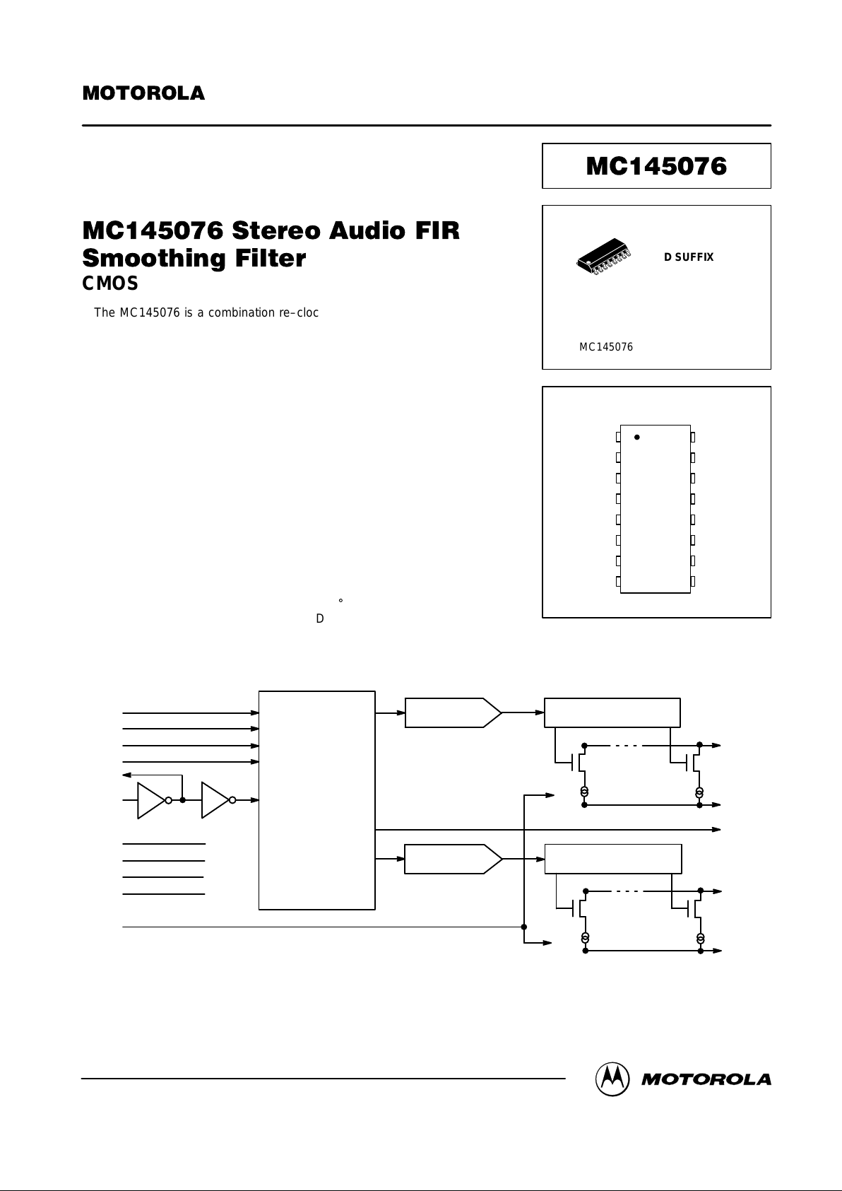
FUNCTIONAL DESCRIPTION
Serial bitstream Digital–to–Analog Converters (DACs)
have become commonplace due to their ability to use over–
sampling techniques to shape quantization noise. This noise
shaping ability enables devices to be built that do not require
the component matching of conventional architectures.
The MC145076 bitstream FIR smoothing filter consists of
two shift registers, two sets of Hamming Window weighted
current source summing networks, and a crystal oscillator inverting buffer.
The current source summing networks are used to implement a Hamming Window function within the MC145076.
Each current source tap sinks a constant current that does
not change with the number of bits that are set in the shift
register. Therefore, each tap acts as a separate single–bit
converter with excellent linearity characteristics. The Hamming window was chosen for the FIR filter coefficients because this allows a slightly better second lobe attenuation
close to the band where the sampling images are the most
troublesome. For a 256 OSR, the MC145076 FIR filter provides greater than 40 dB of stop band attenuation, with
approximately 50 dB of attenuation at the 8x image frequencies. This results in an output with full scale images of less
than – 70 dB and out–of–band noise better than – 60 dB. For
other OSR rates, the filter response scales linearly.
CRYSTAL OSCILLATOR
Provisions for an on–chip crystal oscillator are provided to
insure that the clock will be as clean as possible internal to
the MC145076 where the digital–to–analog conversion occurs, thus assuring maximum performance. An output clock
buffer is provided for driving additional off–chip digital circuitry such as a digital noise shaper, over–sampling FIR filter, or
DSP. The off–chip digital processing ensures that the digital
switching noise on chip is kept to a minimum.
APPLICATIONS
A smoothing filter is required when using a sigma–delta
DAC to reduce the out–of–band noise, and to prevent the
high frequencies from intermodulating to lower frequencies.
Using the MC145076 with its current sink output is easier
than a voltage output filter because it gives a degree of immunity to mutual ground paths between it and the next amplifier.
The circuit shown in Figure 2 is excellent for most applications. However, differential operation does reduce low level
switching noise that appears as second harmonic distortion
and weak background noise. Although a simple resistor on
each current source output to V
DDA
may be adequate for
some applications, the OpAmps provide power supply noise
rejection, and, in Figures 2 and 4, also reduce the signal
swing on the current output pin of the part to further improve
distortion.
Page 5

MC145076
MOTOROLA
5
STBY
DIL
DIR
BCLK
WCLK
+ 5 V
47 F
4640
22 pF 22 pF
200
200 k
16.9344 MHz
1000
2000
1000
1000
MC33077
µ
+
499
499
16151413121110
9
1
2
3
4
5
6
7
8
16151413121110
9
1
2
3
4
5
6
7
8
1000
1000
0.01 F
µ
Ω
–
–
+
+
0.1 F
µ
+
Figure 2. Low Cost +5 V Stereo Audio System, Typically 88 dB S/(N+D)
V
L
V
R
+ 5 V
+ 5 V
* ALL RESISTORS 1%
+ 5 V
10 F
µ
MC145076MC145074
Page 6

MC145076
MOTOROLA
6
STBY
DIL
DIR
BCLK
WCLK
22.5792 MHz
249
249
16151413121110
9
1
2
3
4
5
6
7
8
16151413121110
9
1
2
3
4
5
6
7
8
16151413121110
9
1
2
3
4
5
6
7
8
249
249
1000
1000
1000
1000
1000
+ 5 V
0.01 F
µ
1/6 MC74HC04
10 F
µ
+
10 F
µ
+
1/6 MC74HC04
10 F
µ
+
0.1
µ
F
–
+
–
+
1000
200 k
Ω
Figure 3. Mid Performance Stereo Audio System, Typically 98 dB S/(N+D)
MC145074
MC145076 MC145076
4640
4640
22 pF 22 pF
+ 5 V
+ 5 V
– 5 V
– 5 V
V
R
* ALL RESISTORS 1%
+ 5 V
V
L
MC33077
Page 7

MC145076
MOTOROLA
7
STBY
DIL
DIR
BCLK
WCLK
22.5792 MHz
1000
2000
1000
1000
499
249
16151413121110
1
2
3
4
5
6
7
8
16151413121110
9
1
2
3
4
5
6
7
8
1000
1000
16151413121110
9
1
2
3
4
5
6
7
8
499
249
1000
1000
1000
1000
1000
1000
1000
1000
1000
+ 5 V
0.01 F
µ
1/6 MC74HC04
10 F
µ
+
10 F
µ
+
1/6 MC74HC04
10 F
µ
+
0.1
µ
F
–
–
+
+
–
+
–
+
–
+
–
+
1000
200 k
Ω
Figure 4. High Performance Stereo Audio System, Typically 105 dB S/(N+D)
MC145074
MC145076 MC145076
4640
4640
22 pF 22 pF
+ 5 V
+ 5 V
+ 5 V
+ 5 V
+ 5 V
+ 5 V
– 5 V
– 5 V
V
L
V
R
* ALL RESISTORS 1%
MC33077
+ 5 V
Page 8

MC145076
MOTOROLA
8
SOIC PACKAGE
CASE 751B–05
0.25 (0.010) T B A
M
S S
MIN MINMAX MAX
MILLIMETERS INCHES
DIM
A
B
C
D
F
G
J
K
M
P
R
9.80
3.80
1.35
0.35
0.40
0.19
0.10
0
°
5.80
0.25
10.00
4.00
1.75
0.49
1.25
0.25
0.25
7
°
6.20
0.50
0.386
0.150
0.054
0.014
0.016
0.008
0.004
0
°
0.229
0.010
0.393
0.157
0.068
0.019
0.049
0.009
0.009
7
°
0.244
0.019
1.27 BSC 0.050 BSC
NOTES:
1. DIMENSIONING AND TOLERANCING PER ANSI
Y14.5M, 1982.
2. CONTROLLING DIMENSION: MILLIMETER.
3. DIMENSIONS A AND B DO NOT INCLUDE
MOLD PROTRUSION.
4. MAXIMUM MOLD PROTRUSION 0.15 (0.006)
PER SIDE.
5. DIMENSION D DOES NOT INCLUDE DAMBAR
PROTRUSION. ALLOWABLE DAMBAR
PROTRUSION SHALL BE 0.127 (0.005) TOTAL
IN EXCESS OF THE D DIMENSION AT
MAXIMUM MATERIAL CONDITION.
1
8
916
-A-
-B-
D
16 PL
K
C
G
-T-
SEATING
PLANE
R X 45°
M
J
F
P 8 PL
0.25 (0.010) B
M M
P ACKAGE DIMENSIONS
Motorola reserves the right to make changes without further notice to any products herein. Motorola makes no warranty , representation or guarantee regarding
the suitability of its products for any particular purpose, nor does Motorola assume any liability arising out of the application or use of any product or circuit, and
specifically disclaims any and all liability, including without limitation consequential or incidental damages. “T ypical” parameters which may be provided in Motorola
data sheets and/or specifications can and do vary in different applications and actual performance may vary over time. All operating parameters, including “Typicals”
must be validated for each customer application by customer’s technical experts. Motorola does not convey any license under its patent rights nor the rights of
others. Motorola products are not designed, intended, or authorized for use as components in systems intended for surgical implant into the body, or other
applications intended to support or sustain life, or for any other application in which the failure of the Motorola product could create a situation where personal injury
or death may occur. Should Buyer purchase or use Motorola products for any such unintended or unauthorized application, Buyer shall indemnify and hold Motorola
and its officers, employees, subsidiaries, affiliates, and distributors harmless against all claims, costs, damages, and expenses, and reasonable attorney fees
arising out of, directly or indirectly, any claim of personal injury or death associated with such unintended or unauthorized use, even if such claim alleges that
Motorola was negligent regarding the design or manufacture of the part. Motorola and are registered trademarks of Motorola, Inc. Motorola, Inc. is an Equal
Opportunity/Affirmative Action Employer.
How to reach us:
USA/EUROPE /Locations Not Listed: Motorola Literature Distribution; JAPAN: Nippon Motorola Ltd.; Tatsumi–SPD–JLDC, 6F Seibu–Butsuryu–Center,
P.O. Box 20912; Phoenix, Arizona 85036. 1–800–441–2447 or 602–303–5454 3–14–2 Tatsumi Koto–Ku, Tokyo 135, Japan. 03–81–3521–8315
MFAX: RMF AX0@email.sps.mot.com – TOUCHT ONE 602–244–6609 ASIA/PACIFIC: Motorola Semiconductors H.K. Ltd.; 8B Tai Ping Industrial Park,
INTERNET: http://Design–NET.com 51 Ting Ko k Road, Tai Po, N.T., Hong Kong. 852–26629298
MC145076/D
*MC145076/D*
◊
 Loading...