

Page 1
SEMICONDUCTOR TECHNICAL DATA
Order this document
by MC145050/D
CMOS
These ratiometric 10-bit ADCs have serial interface ports to provide
communication with MCUs and MPUs.
. The 16-bit format can be one continuous 16-bit stream or two intermittent
used
8-bit streams. The converters operate from a single power supply with no
external trimming required. Reference voltages down to 4.0 V are accommodated.
The MC145050 has the same pin out as the 8-bit MC145040 which allows an
external clock (ADCLK) to operate the dynamic A/D conversion sequence. The
MC145051 has the same pin out as the 8-bit MC145041 which has an internal
clock oscillator and an end-of-conversion (EOC) output.
• 1 1 Analog Input Channels with Internal Sample-and-Hold
• Operating Temperature Range: – 40 to 125° C
• Successive Approximation Conversion Time:
MC145050 — 21 µs (with 2.1 MHz ADCLK)
MC145051 — 44 µs Maximum
• Maximum Sample Rate: MC145050 — 38 ks/s
MC145051 — 20.4 ks/s
• Analog Input Range with 5-Volt Supply: 0 to 5 V
• Monotonic with No Missing Codes
• Direct Interface to Motorola SPI and National MICROWIRE Serial Data
Ports
• Digital Inputs/Outputs are TTL, NMOS, and CMOS Compatible
• Low Power Consumption: 14 mW
• Chip Complexity: 1630 Elements (FETs, Capacitors, etc.)
• See Application Note AN1062 for Operation with QSPI
Either a 10- or 16-bit format can be
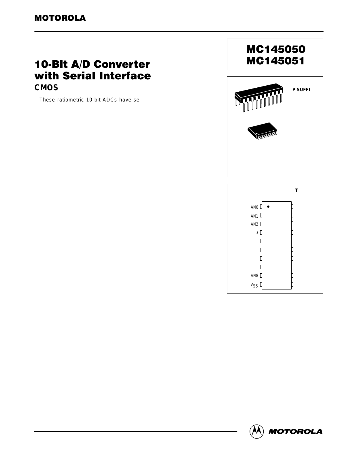
P SUFFIX
PLASTIC
CASE 738
DW SUFFIX
SOG
CASE 751D
ORDERING INFORMATION
MC14505xP Plastic DIP
MC14505xDW SOG Package
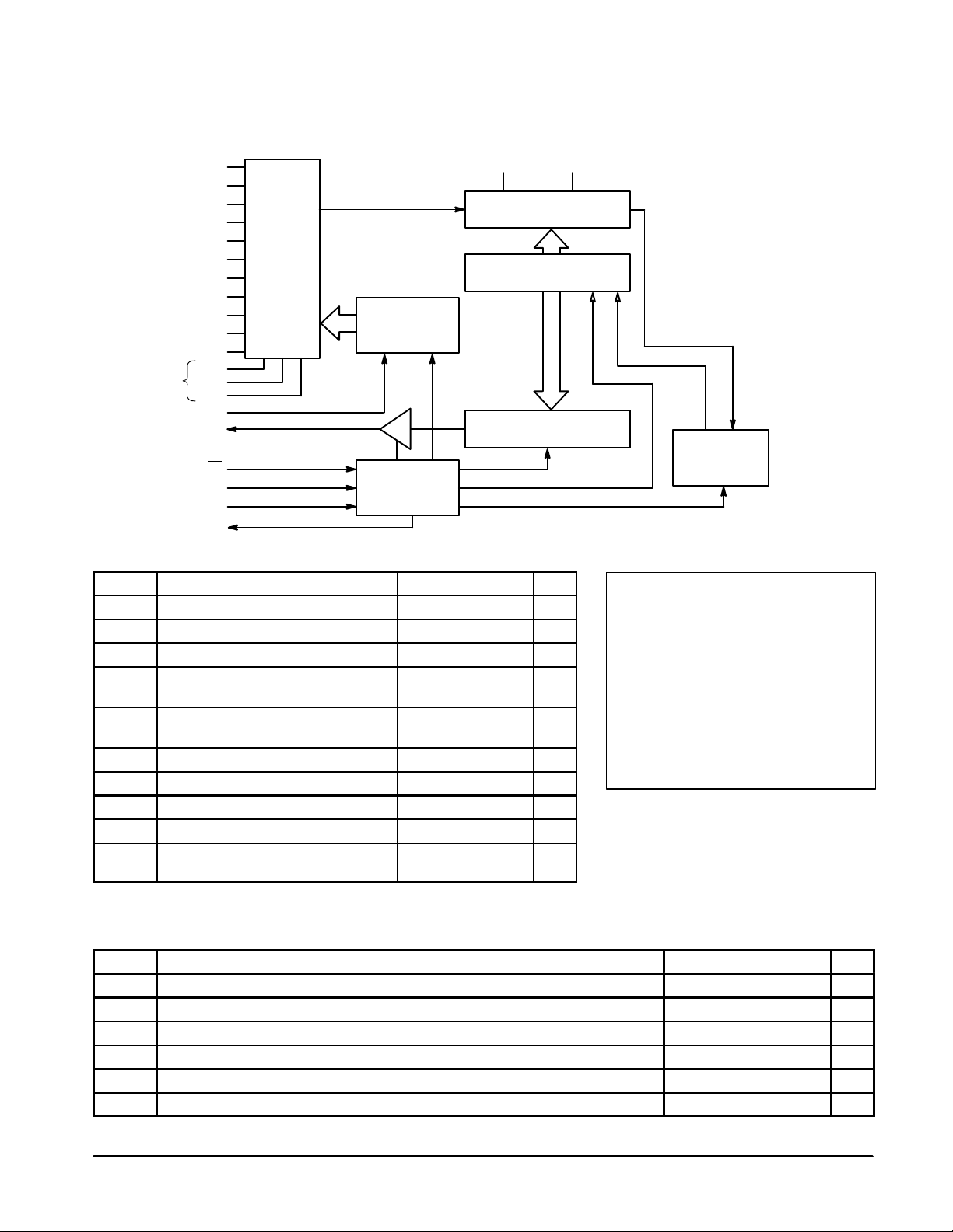
PIN ASSIGNMENT
*ADCLK (MC145050); EOC (MC145051)
AN0
AN1
AN2
AN3
AN4 5
AN5
AN6
AN7
AN8
V
SS
1
2
3
4
6
7
8
9
10
20
19
18
17
16
15
14
13
12
11
V
DD
*
SCLK
D
in
D
out
CS
V
ref
V
AG
AN10
AN9
MICROWIRE is a trademark of National Semiconductor Corp.
REV 2
1/99
MOTOROLA WIRELESS SEMICONDUCTOR
Motorola, Inc. 1998
SOLUTIONS DEVICE DA TA
MC145050 MC145051
1
Page 2
BLOCK DIAGRAM
AN0
AN1
AN2
AN3
AN4
AN5
AN6
AN7
AN8
AN9
AN10
INTERNAL
TEST
VOLTAGES
ADCLK (MC145050 ONLY)
EOC (MC145051 ONLY)
AN11
AN12
AN13
D
D
out
CS
SCLK
1
2
3
4
5
6
ANALOG
7
MUX
8
9
11
12
17
in
16
15
18
19
19
MUX OUT
MUX ADDRESS
REGISTER
DIGITAL CONTROL
LOGIC
V
ref
14 13
10-BIT RC DAC
WITH SAMPLE AND HOLD
SUCCESSIVE APPROXIMA TION
DATA REGISTER
V
REGISTER
ABSOLUTE MAXIMUM RATINGS
Symbol Parameter Value Unit
V
V
V
V
I
IDD, ISSDC Supply Current, VDD and VSS Pins ± 50 mA
T
*Maximum Ratings are those values beyond which damage to the device may occur. Func-
tional operation should be restricted to the Operation Ranges below..
DC Supply Voltage (Referenced to VSS) – 0.5 to + 6.0 V
DD
DC Reference Voltage VAG to VDD + 0.1 V
ref
Analog Ground VSS – 0.1 to V
AG
V
DC Input Voltage, Any Analog or Digital
in
Input
DC Output Voltage VSS – 0.5 to
out
I
DC Input Current, per Pin ± 20 mA
in
DC Output Current, per Pin ± 25 mA
out
Storage Temperature – 65 to 150 °C
stg
T
Lead Temperature, 1 mm from Case for
L
10 Seconds
VSS – 0.5 to
VDD + 0.5
VDD + 0.5
260 °C
ref
V
V
V
AG
PIN 20 = V
PIN 10 = V
This device contains protection circuitry to
guard against damage due to high static
voltages or electric fields. However, precautions must be taken to avoid applications
of any voltage higher than maximum rated
voltages to this high-impedance circuit. For
proper operation, Vin and V
constrained to the range VSS ≤ (Vin or V
VDD.
Unused inputs must always be tied to an
appropriate logic voltage level (e.g., either
VSS or VDD). Unused outputs must be left
open.
DD
SS
AUTO-ZEROED
COMPARATOR
should be
out
out
) ≤
OPERATION RANGES (Applicable to Guaranteed Limits)
Symbol
V
V
V
Vin, V
NOTE: Analog input voltages greater than V
DC Supply Voltage, Referenced to V
DD
DC Reference Voltage VAG + 4.0 to VDD + 0.1 V
ref
Analog Ground VSS – 0.1 to V
AG
V
Analog Input Voltage (See Note) VAG to V
AI
Digital Input Voltage, Output Voltage VSS to V
out
T
Ambient Operating Temperature – 40 to 125 °C
A
descriptions.
Parameter Value Unit
SS
convert to full scale. Input voltages less than VAG convert to zero. See V
ref
MC145050 MC145051
2
4.5 to 5.5 V
– 4.0 V
ref
ref
DD
ref
and VAG pin
V
V
MOTOROLA WIRELESS SEMICONDUCTOR
SOLUTIONS DEVICE DA TA
Page 3
DC ELECTRICAL CHARACTERISTICS
(Voltages Referenced to VSS, Full T emperature and Voltage Ranges per Operation Ranges T able, unless otherwise indicated)
Guaranteed
Symbol
V
IH
V
IL
V
OH
V
OL
I
in
I
OZ
I
DD
I
ref
I
Al
Parameter Test Condition
Minimum High-Level Input Voltage
(Din, SCLK, CS
Maximum Low-Level Input Voltage
(Din, SCLK, CS
Minimum High-Level Output Voltage
(D
, EOC)
out
Minimum Low-Level Output Voltage
(D
, EOC)
out
Maximum Input Leakage Current
(Din, SCLK, CS
Maximum Three-State Leakage Current (D
Maximum Power Supply Current Vin = VSS or VDD, All Outputs Open 2.5 mA
Maximum Static Analog Reference Current (V
Maximum Analog Mux Input Leakage Current between all
deselected inputs and any selected input (AN0 – AN10)
, ADCLK)
, ADCLK)
, ADCLK)
) V
out
) V
ref
I
= – 1.6 mA
out
I
= – 20 µA
out
I
= + 1.6 mA
out
I
= 20 µA
out
Vin = VSS or V
= VSS or V
out
= VDD, VAG = V
ref
VAl = VSS to V
DD
DD
SS
DD
Limit
2.0 V
0.8 V
2.4
VDD – 0.1
0.4
0.1
± 2.5 µA
± 10 µA
100 µA
± 1 µA
A/D CONVERTER ELECTRICAL CHARACTERISTICS
(Full Temperature and Voltage Ranges per Operation Ranges Table; MC145050: 500 kHz ≤ ADCLK ≤ 2.1 MHz, unless otherwise noted)
Guaranteed
Characteristic
Resolution Number of bits resolved by the A/D converter 10 Bits
Maximum Nonlinearity Maximum difference between an ideal and an actual ADC transfer function ± 1 LSB
Maximum Zero Error Difference between the maximum input voltage of an ideal and an actual
ADC for zero output code
Maximum Full-Scale Error Difference between the minimum input voltage of an ideal and an actual
ADC for full-scale output code
Maximum Total Unadjusted Error Maximum sum of nonlinearity, zero error , and full-scale error ± 1 LSB
Maximum Quantization Error Uncertainty due to converter resolution ± 1/2 LSB
Absolute Accuracy Difference between the actual input voltage and the full-scale weighted
equivalent of the binary output code, all error sources included
Maximum Conversion Time Total time to perform a single analog-to-digital conversion MC145050
Data Transfer Time Total time to transfer digital serial data into and out of the device 10 to 16 SCLK
Sample Acquisition Time Analog input acquisition time window 6 SCLK
Minimum Total Cycle Time Total time to transfer serial data, sample the analog input, and perform the
conversion
MC145050: ADCLK = 2.1 MHz, SCLK = 2.1 MHz
MC145051: SCLK = 2.1 MHz
Maximum Sample Rate Rate at which analog inputs may be sampled
MC145050: ADCLK = 2.1 MHz, SCLK = 2.1 MHz
MC145051: SCLK = 2.1 MHz
Definition and Test Conditions
MC145051
Limit
± 1 LSB
± 1 LSB
± 1-1/2 LSB
44
44
26
49
38
20.4
Unit
ADCLK
cycles
cycles
cycles
ks/s
Unit
V
V
µs
µs
MOTOROLA WIRELESS SEMICONDUCTOR
SOLUTIONS DEVICE DA TA
MC145050 MC145051
3
Page 4
AC ELECTRICAL CHARACTERISTICS
(Full Temperature and Voltage Ranges per Operation Ranges Table)
Guaranteed
Figure
1 f Clock Frequency, SCLK (10-bit xfer) Min
1 f Clock Frequency, ADCLK Minimum
1 t
1 t
1, 7 t
1, 7 t
2, 7 t
2, 7 t
3 t
3 t
4, 7, 8 t
5 t
— t
— t
5 t
6, 8 t
1 tr, t
1, 4, 6 – 8 t
— C
— C
NOTES:
1. After the 10th SCLK falling edge (≤ 2 V), at least 1 SCLK rising edge (≥ 2 V) must occur within 38 ADCLKs (MC145050) or 18.5 µs
(MC145051).
2. On the MC145051, a CS
Symbol Parameter
Note: Refer to twH, twL below (10- to 16-bit xfer) Max)
Note: Refer to twH, twL below Maximum
Minimum Clock High Time ADCLK
Minimum Clock Low Time ADCLK
Maximum Propagation Delay, SCLK to D
PHL
Minimum Hold Time, SCLK to D
Maximum Propagation Delay, CS to D
PHZ
Maximum Propagation Delay, CS to D
PZH
Minimum Setup Time, Din to SCLK 100 ns
Minimum Hold Time, SCLK to D
Maximum Delay Time, EOC to D
Minimum Setup Time, CS to SCLK MC145050
Minimum Time Required Between 10th SCLK Falling MC145050
Edge (≤ 0.8 V) and CS
Maximum Delay Between 10th SCLK Falling Edge MC145050
(≤ 2 V) and CS
Minimum Hold Time, Last SCLK to CS 0 ns
Maximum Propagation Delay, 10th SCLK to EOC MC145051 2.35 µs
Maximum Input Rise and Fall Times SCLK
f
Maximum Output Transition Time, Any Output 300 ns
THL
Maximum Input Capacitance AN0 – AN10
in
Maximum Three-State Output Capacitance D
edge may be received immediately after an active transition on the EOC pin.
to Allow a Conversion MC145051
to Abort a Conversion
out
out
out
in
(MSB) MC145051 100 ns
out
PLH
PLZ
PZL
TLH
wH
wL
, t
h
, t
, t
su
h
d
su
CSd
CAs
h
PHL
, t
out
(11- to 16-bit xfer) Min
SCLK
SCLK
out
High-Z 150 ns
Driven MC145050
MC145051
MC145051
MC145051
ADCLK
Din, CS
ADCLK, SCLK, CS
2 ADCLK cycles + 300
2 ADCLK cycles + 425
, D
in
out
Limit
0
Note 1
2.1
500
2.1
190
190
190
190
125 ns
10 ns
2.3
0 ns
2.425
44
Note 2
36
9
1
250
10
55
15
15 pF
Unit
MHz
kHz
MHz
ns
ns
ns
µs
ns
µs
ADCLK
cycles
ADCLK
cycles
µs
ms
ns
µs
pF
MC145050 MC145051
4
MOTOROLA WIRELESS SEMICONDUCTOR
SOLUTIONS DEVICE DA TA
Page 5
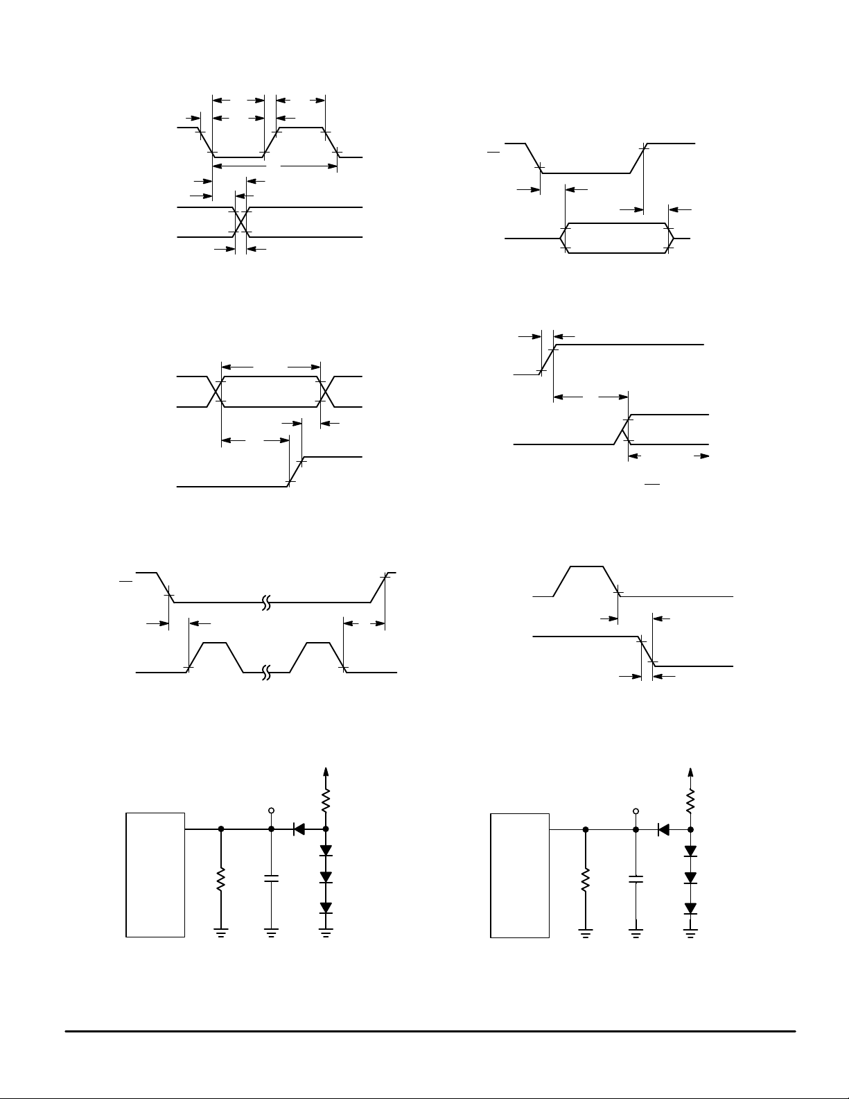
SWITCHING WAVEFORMS
SCLK
D
out
D
in
SCLK
t
f
2.0 V
t
h
t
wL
0.8 V
2.4 V
0.4 V
Figure 1.
VALID
2.0 V
0.8 V
t
su
1/f
t
PLH
t
TLH
, t
, t
t
wH
t
r
PHL
THL
0.8 V
2.0 V
PZL
2.0 V
90%
10%
t
PHZ
, t
PLZ
CS
D
out
0.8 V
2.4 V
0.4 V
t
PZH
, t
Figure 2.
t
TLH
EOC
0.4 V
t
h
D
out
NOTE: D
2.4 V
t
d
2.4 V
0.4 V
VALID MSB
is driven only when CS is active (low).
out
CS
SCLK
DEVICE
UNDER
TEST
0.8 V
D
Figure 3.
t
su
FIRST
CLOCK
Figure 5.
out
12 k 100 pF
TEST
POINT
LAST
CLOCK
V
DD
0.8 V0.8 V
2.18 k
2.0 V
t
h
SCLK
EOC
DEVICE
UNDER
TEST
EOC
Figure 4.
10TH
CLOCK
2.4 V
t
THL
Figure 6.
12 k 50 pF
0.8 V
TEST
POINT
t
0.4 V
PHL
V
DD
2.18 k
Figure 7. T est Circuit
MOTOROLA WIRELESS SEMICONDUCTOR
SOLUTIONS DEVICE DA TA
Figure 8. T est Circuit
MC145050 MC145051
5
Page 6

PIN DESCRIPTIONS
DIGITAL INPUTS AND OUTPUT
The various serial bit-stream formats for the MC145050/51
are illustrated in the timing diagrams of Figures 9 through 14.
Table 1 assists in selection of the appropriate diagram. Note
that the ADCs accept 16 clocks which makes them SPI (Serial Peripheral Interface) compatible.
T able 1. Timing Diagram Selection
No. of Clocks in
Serial Transfer
10 Yes Don’t Care 9
10 No Don’t Care 10
11 to 16 Yes Shorter than Conversion 11
16 No Shorter than Conversion 12
11 to 16 Yes Longer than Conversion 13
16 No Longer than Conversion 14
CS
Active-Low Chip Select Input (Pin 15)
Chip select initializes the chip to perform conversions and
provides 3-state control of the data output pin (D
inactive high, CS
and disables the data input (Din) and serial clock (SCLK)
pins. A high-to-low transition on CS
port and synchronizes it to the MPU data stream. CS can remain active during the conversion cycle and can stay in the
active low state for multiple serial transfers or CS
active high after each transfer. If CS
tween transfers, the length of each transfer is limited to either
10 or 16 SCLK cycles. If CS
tween transfers, each transfer can be anywhere from 10 to
16 SCLK cycles long. See the SCLK pin description for a
more detailed discussion of these requirements.
On the MC145050/51 spurious chip selects caused by
system noise are minimized by the internal circuitry.
Any transitions on the MC145050 CS
as valid only if the level is maintained for a setup time plus
two falling edges of ADCLK after the transition.
Transitions on the MC145051 CS
valid only if the level is maintained for about 2 µs after the
transition.
is inactive high after the 10th SCLK cycle
If CS
and then goes active low before the A/D conversion is complete, the conversion is aborted and
the chip enters the initial state, ready for another
serial transfer/conversion sequence. At this point,
the output data register contains the result from
the conversion before the aborted conversion.
Note that the last step of the A/D conversion sequence is to update the output data register with
the result. Therefore, if CS
attempt to abort the conversion too close to the
end of the conversion sequence, the result register may be corrupted and the chip could be thrown
out of sync with the processor until CS
again (refer to the AC Electrical Characteristics in
the spec tables).
Using
CS
forces D
Serial Transfer
Interval
to the high-impedance state
out
out
Figure
No.
). While
resets the serial data
can be in-
is kept active low be-
is in the inactive high state be-
pin are recognized
pin are recognized as
NOTE
goes active low in an
is toggled
D
out
Serial Data Output of the A/D Conversion Result
(Pin 16)
This output is in the high-impedance state when CS
is in-
active high. When the chip recognizes a valid active low on
, D
CS
is taken out of the high-impedance state and is driv-
out
en with the MSB of the previous conversion result. (For the
first transfer after power-up, data on D
entire transfer.) The value on D
out
is undefined for the
out
changes to the second
most significant result bit upon the first falling edge of SCLK.
The remaining result bits are shifted out in order, with the
LSB appearing on D
upon the ninth falling edge of SCLK.
out
Note that the order of the transfer is MSB to LSB. Upon the
10th falling edge of SCLK, D
allowed by CS
) so that transfers of more than 10 SCLKs read
is immediately driven low (if
out
zeroes as the unused LSBs.
When CS
is held active low between transfers, D
out
is driven from a low level to the MSB of the conversion result for
three cases: Case 1 — upon the 16th SCLK falling edge if
the transfer is longer than the conversion time (Figure 14);
Case 2 — upon completion of a conversion for a 16-bit transfer interval shorter than the conversion (Figure 12); Case 3
— upon completion of a conversion for a 10-bit transfer (Figure 10).
D
in
Serial Data Input (Pin 17)
The four-bit serial input stream begins with the MSB of the
analog mux address (or the user test mode) that is to be converted next. The address is shifted in on the first four rising
edges of SCLK. After the four mux address bits have been
received, the data on Din is ignored for the remainder of the
present serial transfer. See Table 2 in Applications In-
formation.
SCLK
Serial Data Clock (Pin 18)
This clock input drives the internal I/O state machine to
perform three major functions: (1) drives the data shift registers to simultaneously shift in the next mux address from the
Din pin and shift out the previous conversion result on the
D
pin, (2) begins sampling the analog voltage onto the RC
out
DAC as soon as the new mux address is available, and (3)
transfers control to the A/D conversion state machine (driven
by ADCLK) after the last bit of the previous conversion result
has been shifted out on the D
out
pin.
The serial data shift registers are completely static, allowing SCLK rates down to the dc. There are some cases, however, that require a minimum SCLK frequency as discussed
later in this section. SCLK need not be synchronous to
ADCLK. At least ten SCLK cycles are required for each simultaneous data transfer. If the 16-bit format is used, SCLK
can be one continuous 16-bit stream or two intermittent 8-bit
streams. After the serial port has been initiated to perform a
serial transfer*, the new mux address is shifted in on the first
*The serial port can be initiated in three ways: (1) a recognized CS
falling edge, (2) the end of an A/D conversion if the port is performing either a 10-bit or a 16-bit “shorter-than-conversion” transfer
with CS
active low between transfers, and (3) the 16th falling edge
of SCLK if the port is performing 16-bit “longer-than-conversion”
transfers with CS
active low between transfers.
MC145050 MC145051
6
MOTOROLA WIRELESS SEMICONDUCTOR
SOLUTIONS DEVICE DA TA
Page 7

four rising edges of SCLK, and the previous 10-bit conversion result is shifted out on the first nine falling edges of
SCLK. After the fourth rising edge of SCLK, the new mux address is available; therefore, on the next edge of SCLK (the
fourth falling edge), the analog input voltage on the selected
mux input begins charging the RC DAC and continues to do
so until the tenth falling edge of SCLK. After this tenth SCLK
edge, the analog input voltage is disabled from the RC DAC
and the RC DAC begins the “hold” portion of the A/D conversion sequence. Also upon this tenth SCLK edge, control of
the internal circuitry is transferred to ADCLK which drives the
successive approximation logic to complete the conversion.
If 16 SCLK cycles are used during each transfer, then there
is a constraint on the minimum SCLK frequency . Specifically,
there must be at least one rising edge on SCLK before the
A/D conversion is complete. If the SCLK frequency is too low
and a rising edge does not occur during the conversion, the
chip is thrown out of sync with the processor and CS
to be toggled in order to restore proper operation. If 10
SCLKs are used per transfer, then there is no lower frequency limit on SCLK. Also note that if the ADC is operated such
that CS
of SCLK cycles per transfer can be anything between 10 and
16 cycles, but the “rising edge” constraint is still in effect if
more than 10 SCLKs are used. (If CS
multiple transfers, the number of SCLK cycles must be either
10 or 16.)
is inactive high between transfers, then the number
stays active low for
needs
by $A. Table 2 shows the input format for a 16-bit stream.
The mux features a break-before-make switching structure
to minimize noise injection into the analog inputs. The source
resistance driving these inputs must be v 1 kΩ.
During normal operation, leakage currents through the
analog mux from unselected channels to a selected channel
and leakage currents through the ESD protection diodes on
the selected channel occur. These leakage currents cause
an offset voltage to appear across any series source resistance on the selected channel. Therefore, any source resistance greater than 1 kΩ (Motorola test condition) may induce
errors in excess of guaranteed specifications.
There are three tests available that verify the functionality
of all the control logic as well as the successive approximation comparator. These tests are performed by addressing
$B, $C, or $D and they convert a voltage of (V
VAG, or V
ly by sampling V
the RC DAC during the sample phase. Addressing $B, $C, or
$D produces an output of $200 (half scale), $000, or $3FF
(full scale), respectively, if the converter is functioning properly. However, deviation from these values occurs in the
presence of sufficient system noise (external to the chip) on
VDD, VSS, V
POWER AND REFERENCE PINS
, respectively. The voltages are obtained internal-
ref
or VAG onto the appropriate elements of
ref
, or VAG.
ref
+ VAG)/2,
ref
ADCLK
A/D Conversion Clock Input (Pin 19, MC145050 Only)
This pin clocks the dynamic A/D conversion sequence,
and may be asynchronous to SCLK. Control of the chip
passes to ADCLK after the tenth falling edge of SCLK. Control of the chip is passed back to SCLK after the successive
approximation conversion sequence is complete (44 ADCLK
cycles), or after a valid chip select is recognized. ADCLK
also drives the CS
tions on CS
two falling edges of ADCLK. The source driving ADCLK must
be free running.
EOC
End-of-Conversion Output (Pin 19, MC145051 Only)
EOC goes low on the tenth falling edge of SCLK. A low-tohigh transition on EOC occurs when the A/D conversion is
complete and the data is ready for transfer.
ANALOG INPUTS AND TEST MODE
AN0 through AN10
Analog Multiplexer Inputs (Pins 1 – 9, 11, 12)
The input AN0 is addressed by loading $0 into the mux address register. AN1 is addressed by $1, AN2 by $2, …, AN10
recognition logic. The chip ignores transi-
unless the state remains for a setup time plus
VSS and V
Device Supply Pins (Pins 10 and 20)
VSS is normally connected to digital ground; VDD is connected to a positive digital supply voltage. Low frequency
(VDD – VSS) variations over the range of 4.5 to 5.5 volts do
not affect the A/D accuracy. (See the Operations Ranges
Table for restrictions on V
VSS.) Excessive inductance in the VDD or VSS lines, as on
automatic test equipment, may cause A/D offsets > ± 1 LSB.
Use of a 0.1 µF bypass capacitor across these pins is recommended.
VAG and V
Analog Reference V oltage Pins (Pins 13 and 14)
Analog reference voltage pins which determine the lower
and upper boundary of the A/D conversion. Analog input voltages ≥ V
≤ VAG produce an output of zero. CAUTION: The analog
input voltage must be ≥ VSS and ≤ VDD. The A/D conversion
result is ratiometric to V
noise-free as possible to avoid degradation of the A/D conversion. Ideally, V
nected to the voltage supply driving the system’s
transducers. Use of a 0.22 µF bypass capacitor across these
pins is strongly urged.
DD
and VAG relative to VDD and
ref
ref
produce a full scale output and input voltages
ref
– VAG. V
ref
and VAG should be single-point con-
ref
and VAG must be as
ref
MOTOROLA WIRELESS SEMICONDUCTOR
SOLUTIONS DEVICE DA TA
MC145050 MC145051
7
Page 8

CS
D
out
SCLK
D
in
EOC
CS
D9 – MSB
MSB
D8 D7 D6 D5 D4 D3 D2 D1 D0 D9
12345678910 1
SAMPLE ANALOG INPUT
A3 A2 A1 A0
SHIFT IN NEW MUX ADDRESS,
SIMULTANEOUSLY SHIFT OUT PREVIOUS CONVERSION VALUE
HIGH IMPEDANCE
A/D CONVERSION
INTERV AL
RE-INITIALIZEINITIALIZE
Figure 9. Timing for 10-Clock Transfer Using CS*
MUST BE HIGH ON POWER UP
A3
D
SCLK
EOC
D9 – MSB D8 D7 D6 D5 D4 D3 D2 D1 D0 D9
out
D
in
INITIALIZE
12345678910 1
SAMPLE ANALOG INPUT
A3 A2 A1 A0 A3
MSB
SHIFT IN NEW MUX ADDRESS,
SIMULTANEOUSLY SHIFT OUT PREVIOUS CONVERSION VALUE
LOW LEVEL
A/D CONVERSION
INTERV AL
Figure 10. Timing for 10-Clock Transfer Not Using CS*
NOTES:
1. D9, D8, D7, …, D0 = the result of the previous A/D conversion.
2. A3, A2, A1, A0 = the mux address for the next A/D conversion.
*This figure illustrates the behavior of the MC145051. The MC145050 behaves identically except there is no EOC signal and the conversion time
is 44 ADCLK cycles (user-controlled time).
MC145050 MC145051
8
MOTOROLA WIRELESS SEMICONDUCTOR
SOLUTIONS DEVICE DA TA
Page 9

D9
HIGH
IMPEDANCE
LOW
LEVEL
1
D9
1
A3
RE-INITIALIZE
INTERV AL
A/D CONVERSION
LOW LEVEL
12 13 14 15
A3A3 A2 A1 A0
A/D CONVERSION INTERV AL
CS
D8 D7 D6 D5 D4 D3 D2 D1 D0
D9 – MSB
out
D
SAMPLE ANALOG INPUT
123456789101116
SCLK
SHIFT IN NEW MUX ADDRESS,
SIMULTANEOUSLY SHIFT OUT PREVIOUS CONVERSION VALUE
A3 A2 A1 A0
Figure 11. T iming for 11- to 16-Clock Transfer Using CS* (Serial Transfer Interval Shorter than Conversion)
in
D
EOC
INITIALIZE
MUST BE HIGH ON POWER UP
D9 – MSB D8 D7 D6 D5 D4 D3 D2 D1 D0
CS
D
out
SAMPLE ANALOG INPUT
1234567891011 16
SCLK
SHIFT IN NEW MUX ADDRESS,
SIMULTANEOUSLY SHIFT OUT PREVIOUS CONVERSION VALUE
MSB
in
D
EOC
Figure 12. Timing for 16-Clock Transfer Not Using CS* (Serial Transfer Interval Shorter Than Conversion)
D9, D8, D7, . . . , D0 = the result of the previous A/D conversion.
A3, A2, A1, A0 = the mux address for the next A/D conversion.
NOTES:
INITIALIZE
*This figure illustrates the behavior of the MC145051. The MC145050 behaves identically except there is no EOC signal and the conversion time is 44 ADCLK cycles (user-controlled time).
MOTOROLA WIRELESS SEMICONDUCTOR
SOLUTIONS DEVICE DA TA
MC145050 MC145051
9
Page 10

D9
HIGH
IMPEDANCE
LOW
LEVEL
1
D9
1
2
NOTE
A3
RE-INITIALIZE
A/D
INTERVAL
CONVERSION
LOW LEVEL
A3
NOTE 2
CS
D8 D7 D6 D5 D4 D3 D2 D1 D0
D9 – MSB
out
D
SAMPLE ANALOG INPUT
123456789101116
SCLK
12 13 14 15
SHIFT IN NEW MUX ADDRESS,
SIMULTANEOUSLY SHIFT OUT PREVIOUS CONVERSION VALUE
A3 A2 A1 A0
Figure 13. Timing for 1 1- to 16-Clock Transfer Using CS* (Serial Transfer Interval Longer Than Conversion)
in
D
EOC
INITIALIZE
MUST BE HIGH ON POWER UP
D8 D7 D6 D5 D4 D3 D2 D1 D0
D9 – MSB
SAMPLE ANALOG INPUT
1234567891011 16
A3 A2 A1 A0
MSB
INTERV AL
A/D CONVERSION
SHIFT IN NEW MUX ADDRESS,
Figure 14. Timing for 16-Clock T ransfer Not Using CS* (Serial Transfer Interval Longer Than Conversion)
SIMULTANEOUSLY SHIFT OUT PREVIOUS CONVERSION VALUE
MC145050 MC145051
10
CS
D
out
SCLK
in
D
EOC
INITIALIZE
MOTOROLA WIRELESS SEMICONDUCTOR
SOLUTIONS DEVICE DA TA
D9, D8, D7, . . . , D0 = the result of the previous A/D conversion.
A3, A2, A1, A0 = the mux address for the next A/D conversion.
NOTES:
1. This figure illustrates the behavior of the MC145051. The MC145050 behaves identically except there is no EOC signal and the conversion time is 44 ADCLK cycles (user-controlled time).
2. The 11th SCLK rising edge must occur before the conversion is complete. Otherwise the serial port is thrown out of sync with the microprocessor for the remainder of the transfer.
*NOTES:
Page 11

APPLICATIONS INFORMATION
DESCRIPTION
This example application of the MC145050/MC145051
ADCs interfaces three controllers to a microprocessor and
processes data in real-time for a video game. The standard
joystick X-axis (left/right) and Y-axis (up/down) controls as
well as engine thrust controls are accommodated.
Figure 15 illustrates how the MC145050/MC145051 is
used as a cost-effective means to simplify this type of circuit
design. Utilizing one ADC, three controllers are interfaced to
a CMOS or NMOS microprocessor with a serial peripheral interface (SPI) port. Processors with National Semiconductor’s
MICROWIRE serial port may also be used. Full duplex
operation optimizes throughput for this system.
DIGITAL DESIGN CONSIDERATIONS
Motorola’s MC68HC05C4 CMOS MCU may be chosen to
reduce power supply size and cost. The NMOS MCUs may
be used if power consumption is not critical. A VDD or V
0.1 µF bypass capacitor should be closely mounted to the
ADC.
Both the MC145050 and MC145051 accommodate all the
analog system inputs. The MC145050, when used with a
2 MHz MCU, takes 27 µs to sample the analog input, perform the conversion, and transfer the serial data at 2 MHz.
Forty-four ADCLK cycles (2 MHz at input pin 19) must be
provided and counted by the MCU before reading the ADC
results. The MC145051 has the end-of-conversion (EOC)
signal (at output pin 19) to define when data is ready , but has
a slower 49 µs cycle time. However, the 49 µs is constant for
serial data rates of 2 MHz independent of the MCU clock frequency. Therefore, the MC145051 may be used with the
CMOS MCU operating at reduced clock rates to minimize
power consumption without severely sacrificing ADC cycle
times, with EOC being used to generate an interrupt. (The
MC145051 may also be used with MCUs which do not
provide a system clock.)
ANALOG DESIGN CONSIDERATIONS
Controllers with output impedances of less than 1 kΩ may
be directly interfaced to these ADCs, eliminating the need for
buffer amplifiers. Separate lines connect the V
pins on the ADC with the controllers to provide isolation from
system noise.
Although not indicated in Figure 15, the V
output lines may need to be shielded, depending on their
ref
and controller
ref
and V
SS
AG
length and electrical environment. This should be verified
during prototyping with an oscilloscope. If shielding is
required, a twisted pair or foil-shielded wire (not coax) is
appropriate for this low frequency application. One wire of
the pair or the shield must be VAG.
A reference circuit voltage of 5 volts is used for this application. The reference circuitry may be as simple as tying
VAG to system ground and V
ply. (See Figure 16.) However, the system power supply
noise may require that a separate supply be used for the voltage reference. This supply must provide source current for
V
as well as current for the controller potentiometers.
ref
A bypass capacitor of approximately 0.22 µF across the
V
and VAG pins is recommended. These pins are adjacent
ref
on the ADC package which facilitates mounting the capacitor
very close to the ADC.
SOFTWARE CONSIDERATIONS
The software flow for acquisition is straightforward. The
nine analog inputs, AN0 through AN8, are scanned by reading the analog value of the previously addressed channel
into the MCU and sending the address of the next channel to
be read to the ADC, simultaneously .
If the design is realized using the MC145050, 44 ADCLK
cycles (at pin 19) must be counted by the MCU to allow time
for A/D conversion. The designer utilizing the MC145051 has
the end-of-conversion signal (at pin 19) to define the conversion interval. EOC may be used to generate an interrupt,
which is serviced by reading the serial data from the ADC.
The software flow should then process and format the data,
and transfer the information to the video circuitry for updating
the display.
When these ADCs are used with a 16-bit (2-byte) transfer ,
there are two types of offsets involved. In the first type of offset, the channel information sent to the ADCs is offset by 12
bits. That is, in the 16-bit stream, only the first 4 bits (4 MSBs)
contain the channel information. The balance of the bits are
don’t cares. This results in 3 don’t-care nibbles, as shown in
Table 2. The second type of offset is in the conversion result
returned from the ADCs; this is offset by 6 bits. In the 16-bit
stream, the first 10 bits (10 MSBs) contain the conversion
results. The last 6 bits are zeroes. The hexadecimal result is
shown in the first column of Table 3. The second column
shows the result after the offset is removed by a microprocessor routine. If the 16-bit format is used, these ADCs can
transfer one continuous 16-bit stream or two intermittent 8-bit
streams.
to the system’s positive sup-
ref
MOTOROLA WIRELESS SEMICONDUCTOR
SOLUTIONS DEVICE DA TA
MC145050 MC145051
11
Page 12

Table 2. Programmer’s Guide for 16-Bit Transfers:
Input Code
Table 3. Programmer’s Guide for 16-Bit Transfers:
Output Code
Input
Address
in Hex
$0XXX
$1XXX
$2XXX
$3XXX
$4XXX
$5XXX
$6XXX
$7XXX
$8XXX
$9XXX
$AXXX
$BXXX
$CXXX
$DXXX
$EXXX
$FXXX
5 VOLT
REFERENCE
CIRCUIT
Channel to be
Converted Next
AN0
AN1
AN2
AN3
AN4
AN5
AN6
AN7
AN8
AN9
AN10
AN11
AN12
AN13
None
None
Comment
Pin 1
Pin 2
Pin 3
Pin 4
Pin 5
Pin 6
Pin 7
Pin 8
Pin 9
Pin 11
Pin 12
Half Scale Test: Output = $8000
Zero Test: Output = $0000
Full Scale Test: Output = $FFC0
Not Allowed
Not Allowed
LEFT/RIGHT
CONTROLLER
#1
CONTROLLER
#2
CONTROLLER
#3
UP/DOWN
ENGINE THRUST
LEFT/RIGHT
UP/DOWN
ENGINE THRUST
LEFT/RIGHT
UP/DOWN
ENGINE THRUST
0.22 µF
Conversion
Result Without
Offset Removed
$0000
$0040
$0080
$00C0
$0100
$0140
$0180
$01C0
$0200
$0240
$0280
$02C0
L
$FF40
$FF80
$FFC0
+ 5 V
V
DD
ADC
MC145050
MC145051
V
V
AN0
AN1
AN2
AN3
AN4
AN5
AN6
AN7
AN8
AG
ref
Offset Removed
0.1
AN9
AN10
V
SS
Conversion
Result With
$0000
$0001
$0002
$0003
$0004
$0005
$0006
$0007
$0008
$0009
$000A
$000B
L
$03FD
$03FE
$03FF
µ
F
CS
D
in
SCLK
D
out
ADCLK
(MC145050)
EOC
(MC145051)
Value
Zero
Zero + 1 LSB
Zero + 2 LSBs
Zero + 3 LSBs
Zero + 4 LSBs
Zero + 5 LSBs
Zero + 6 LSBs
Zero + 7 LSBs
Zero + 8 LSBs
Zero + 9 LSBs
Zero + 10 LSBs
Zero + 11 LSBs
L
Full Scale – 2 LSBs
Full Scale – 1 LSB
Full Scale
µ
P
SPI PORT
VIDEO
CIRCUITRY
MC145050 MC145051
12
VIDEO
MONITOR
Figure 15. Joystick Interface
MOTOROLA WIRELESS SEMICONDUCTOR
SOLUTIONS DEVICE DA TA
Page 13

DIGITAL + V
Instruction
SPI
Device
ANALOG + V
DO NOT CONNECT
AT IC
V
ref
V
DD
5 V
SUPPLY
TO
JOYSTICKS
ANALOG GND
DIGITAL GND
V
AG
MC145050
MC145051
V
SS
DO NOT CONNECT
AT IC
0.1 µF0.22 µF
Figure 16. Alternate Configuration Using the Digital Supply for the Reference Voltage
Compatible Motorola MCUs/MPUs
This is not a complete listing of Motorola’s MCUs/MPUs.
Contact your Motorola representative if you need
Instruction
Set
M6805 2096
M68000 — — — MC68HC000
SPI = Serial Peripheral Interface.
SCI = Serial Communication Interface.
High Speed.
Low Power.
additional information.
Memory (Bytes)
ROM EEPROM
2096
4160
4160
8K
4160
8K
7700
—
—
—
—
—
—
—
—
—
4160
SPI
SCI
Yes
Yes
Yes
Yes
Yes
Yes
Yes
—
—
Device
Number
MC68HC05C2
MC68HC05C3
MC68HC05C4
MC68HSC05C5
MC68HSC05C8
MC68HCL05C4
MC68HCL05C8
MC68HC05C8
MC68HC805C5
MOTOROLA WIRELESS SEMICONDUCTOR
SOLUTIONS DEVICE DA TA
MC145050 MC145051
13
Page 14

P ACKAGE DIMENSIONS
PLASTIC DIP
P SUFFIX
CASE 738-03
-T-
SEATING
PLANE
-A-
1120
B
110
C
K
E
N
GF
D
20 PL
0.25 (0.010) T A
M M
L
J 20 PL
0.25 (0.010) T B
M
M M
NOTES:
1. DIMENSIONING AND TOLERANCING PER ANSI
Y14.5M, 1982.
2. CONTROLLING DIMENSION: INCH.
3. DIMENSION L TO CENTER OF LEAD WHEN
FORMED PARALLEL.
4. DIMENSION B DOES NOT INCLUDE MOLD
FLASH.
INCHES MILLIMETERS
MIN MINMAX MAX
DIM
A
B
C
D
E
F
G
J
K
L
M
N
1.010
0.240
0.150
0.015
0.050 BSC
0.050
0.100 BSC
0.008
0.110
0.300 BSC
°
0
0.020
1.070
0.260
0.180
0.022
0.070
0.015
0.140
15
0.040
°
25.66
6.10
3.81
0.39
1.27 BSC
1.27
2.54 BSC
0.21
2.80
7.62 BSC
°
0
0.51
27.17
6.60
4.57
0.55
1.77
0.38
3.55
15
1.01
°
MC145050 MC145051
14
MOTOROLA WIRELESS SEMICONDUCTOR
SOLUTIONS DEVICE DA TA
Page 15

SOG PACKAGE
DW SUFFIX
CASE 751D-04
-A-
1120
-B-
P 10 PL
0.010 (0.25) B
110
D 20 PL
0.010 (0.25)
M
T
BA
S S
J
F
C
-T-
G 18 PL
SEATING
PLANE
K
M M
NOTES:
1. DIMENSIONING AND TOLERANCING PER
ANSI Y14.5M, 1982.
2. CONTROLLING DIMENSION: MILLIMETER.
3. DIMENSIONS A AND B DO NOT INCLUDE
MOLD PROTRUSION.
4. MAXIMUM MOLD PROTRUSION 0.150 (0.006)
PER SIDE.
5. DIMENSION D DOES NOT INCLUDE DAMBAR
PROTRUSION. ALLOWABLE DAMBAR
PROTRUSION SHALL BE 0.13 (0.005) TOTAL IN
EXCESS OF D DIMENSION AT MAXIMUM
MATERIAL CONDITION.
MILLIMETERS INCHES
MIN MINMAX MAX
DIM
12.65
A
7.40
B
2.35
C
0.35
D
0.50
R X 45°
M
F
1.27 BSC 0.050 BSC
G
0.25
J
0.10
K
0
M
°
P
10.05
R
0.25
12.95
7.60
2.65
0.49
0.90
0.32
0.25
7
10.55
0.75
0.499
0.510
0.292
0.299
0.093
0.104
0.014
0.019
0.020
0.035
0.010
0.012
0.004
0.009
0
7
°
°
°
0.395
0.010
0.415
0.029
Motorola reserves the right to make changes without further notice to any products herein. Motorola makes no warranty , representation or guarantee regarding
the suitability of its products for any particular purpose, nor does Motorola assume any liability arising out of the application or use of any product or circuit, and
specifically disclaims any and all liability, including without limitation consequential or incidental damages. “T ypical” parameters which may be provided in Motorola
data sheets and/or specifications can and do vary in different applications and actual performance may vary over time. All operating parameters, including “Typicals”
must be validated for each customer application by customer’s technical experts. Motorola does not convey any license under its patent rights nor the rights of
others. Motorola products are not designed, intended, or authorized for use as components in systems intended for surgical implant into the body, or other
applications intended to support or sustain life, or for any other application in which the failure of the Motorola product could create a situation where personal injury
or death may occur. Should Buyer purchase or use Motorola products for any such unintended or unauthorized application, Buyer shall indemnify and hold Motorola
and its officers, employees, subsidiaries, affiliates, and distributors harmless against all claims, costs, damages, and expenses, and reasonable attorney fees
arising out of, directly or indirectly, any claim of personal injury or death associated with such unintended or unauthorized use, even if such claim alleges that
Motorola was negligent regarding the design or manufacture of the part. Motorola and are registered trademarks of Motorola, Inc. Motorola, Inc. is an Equal
Opportunity/Affirmative Action Employer.
Mfax is a trademark of Motorola, Inc.
How to reach us:
USA/EUROPE/Locations Not Listed: Motorola Literature Distribution; JAPAN: Motorola Japan Ltd.; SPD, Strategic Planning Office, 141,
P.O. Box 5405, Denver, Colorado 80217. 1–303–675–2140 or 1–800–441–2447 4–32–1 Nishi–Gotanda, Shinagawa–ku, Tokyo, Japan. 81–3–5487–8488
Customer Focus Center: 1–800–521–6274
Mfax: RMFAX0@email.sps.mot.com – TOUCHTONE 1–602–244–6609 ASIA/ PACIFIC: Motorola Semiconductors H.K. Ltd.; 8B Tai Ping Industrial Park,
Moto rola Fax Back Sys tem – US & Canada ONLY 1–800–774–1848 51 Ting Kok Road, Tai Po, N.T., Hong Kong. 852–26629298
– http://sps.motorola.com/mfax/
HOME PAGE: http://motorola.com/sps/
MOTOROLA WIRELESS SEMICONDUCTOR
◊
MC145050 MC145051
MC145050/D
SOLUTIONS DEVICE DA TA
15
 Loading...