

Page 1
SEMICONDUCTOR TECHNICAL DATA
Order this document
by MC145003/D
Product Preview
CMOS
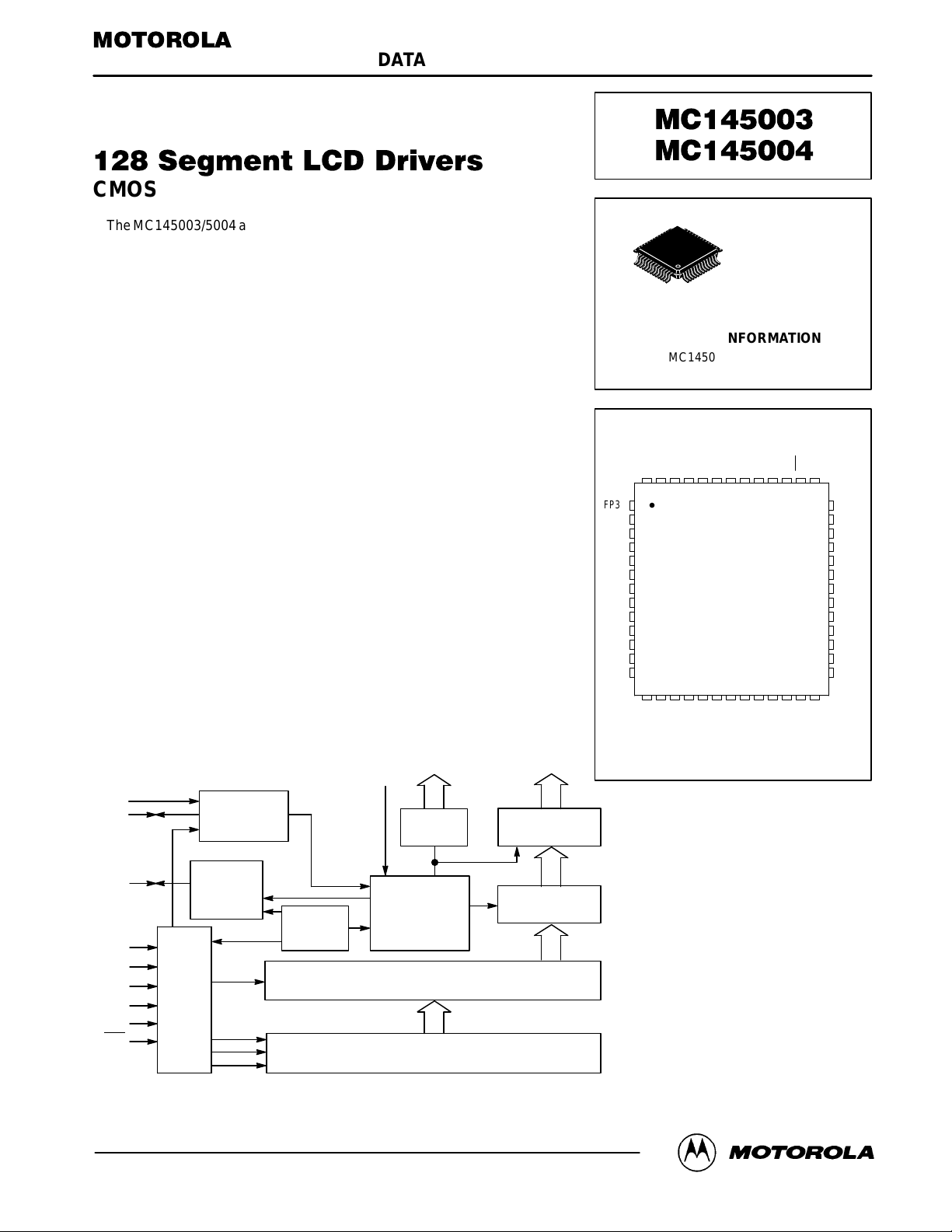
The MC145003/5004 are 128–segment, multiplexed–by–four LCD Drivers.
The two devices are functionally the same except for their data input protocols. The MC145003 uses an SPI data input protocol which is directly compatible with that of the MC6805 family of microcomputers. Using a minimal
amount of software (see example), the device may be interfaced to the
MC68HCXX product families. The MC145004 has a IIC interface and has essentially the same protocol, except that the device sends an acknowledge bit
back to the transmitter after each eight–bit byte is received. MC145004 also
has a “read mode”, whereby data sent to the device may be retrieved via the
IIC bus.
The MC145003/MC145004 drives the liquid–crystal displays in a multiplexed–by–four configuration. The device accepts data from a microprocessor or other serial data source to drive one segment per bit. The chip does not
have a decoder, allowing for the flexibility of formatting the segment data
externally.
Devices are independently addressable via a two–wire (or three–wire)
communication link which can be common with other MC145003/MC145004
and/or other peripheral devices.
• Drives 128 Segments Per Package
• Devices May Be Cascaded for Larger LCD Applications
• May Be Used with the Following LCDs: Segmented Alphanumeric,
Bar Graph, Dot Matrix, Custom
• Quiscent Supply Current: 85 µA @ 2.8 V V
• Operating Voltage Range: 2.8 to 5.5 V
• Operating Temperature Range: –40 to 85°C
• Separate Access to LCD Drive Section’s Supply Voltage to Allow for
Temperature Compensation
• See Application Notes AN1066 and AN442
BLOCK DIAGRAM
DD
1
52
ORDERING INFORMATION
MC145003FU QFP
MC145004FU QFP
PIN ASSIGNMENT
DD
V
NC
OSC1
OSC2
BP1
BP2
52 51 50 49 48 47 46 45 44 43 42 41 40
FP32
1
FP31
2
FP30
3
FP29
4
FP28
5
FP27
6
FP26
7
FP25
8
FP24
9
FP23
10
FP22
11
FP21
12
FP20
13
14 15 16 17 18 19 20 21 22 23 24 25 26
NC
FP19
FP18
FP17
FP16
FP15
V
FU SUFFIX
CASE 848B
BP4A0A1A2ENB
BP3
SS
V
LCD
FP14
FP13
QFP
FP12
NC
39
D
in
38
DCLK
37
FS
36
FP1
35
FP2
34
FP3
33
FP4
32
FP5
31
FP6
30
FP7
29
FP8
28
FP9
27
FP10
NC
FP11
BP1–BP4 FP1–FP32
V
LCD
OSC1
OSC2
FS
DCLK
D
in
A0
A1
A2
ENB
This document contains information on a new product under development. Motorola reserves the right to change or discontinue this product without notice.
Motorola, Inc. 1994
OSCILLA TOR
FRAME
SYNC
GENERAT OR
DATA AND ADDRESS
CONTROL AND TIMING
POR
DRIVERS DRIVERS
LCD VOLTAGE
WAVEFORM
AND TIMING
GENERAT OR
128–BIT LATCH
128–BIT SHIFT REGISTER
128 – 32
MULTIPLEX
REV 1
12/94
NC = NO CONNECTION
Page 2
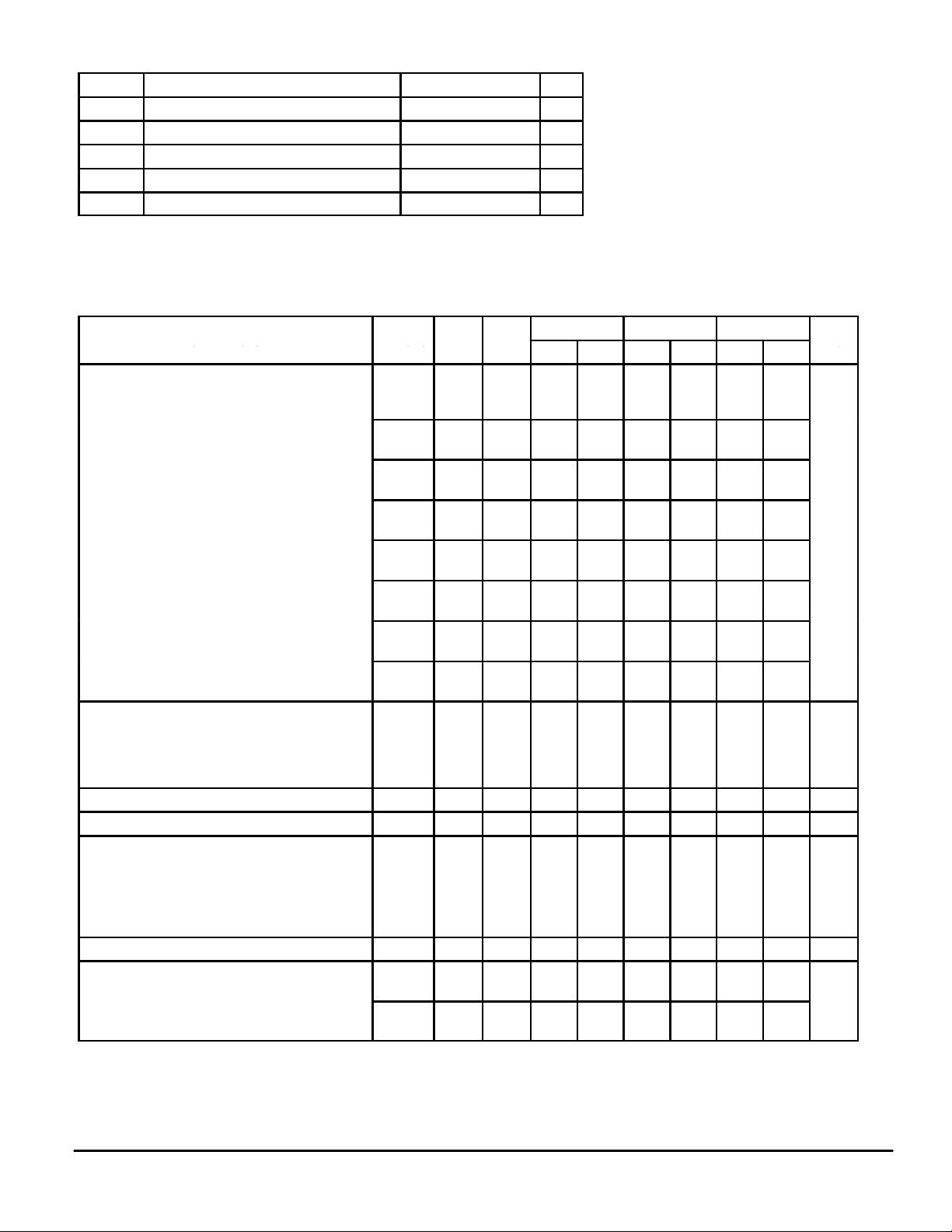
ABSOLUTE MAXIMUM RATINGS (Voltages Referenced to V
V
DD
V
LCD
Symbol
V
DD
V
in
Vin
osc
I
in
T
stg
DC Supply Voltage – 0.5 to + 6.5 V
Input Voltage, Din, and Data Clock – 0.5 to 15 V
Input Voltage, OSCin of Master – 0.5 to VDD + 0.5 V
DC Input Current, per Pin ± 10 mA
Storage Temperature Range – 65 to + 150 °C
Parameter Value Unit
SS
)
*Maximum Ratings are those values beyond which damage to the device may occur . Func-
tional operation should be restricted to the limits in the Electrical Characteristics tables or
Pin Descriptions section.
This device contains protection circuitry
to guard against damage due to high static
voltages or electric fields. However, precautions must be taken to avoid applications of
any voltage higher than maximum rated
voltages to this high–impedance circuit.
ELECTRICAL CHARACTERISTICS (Voltages Referenced to V
Characteristic Symbol
Output Drive Current — Frontplanes
Supply Currents (f
Input Current I
Input Capacitance C
Frequencies
OSC2 Frequency @ R1; R1 = 200 kΩ
OSC2 Frequency @ R2; R2 = 996 kΩ
Average DC Offset Voltage (BP Relative to FP) V
Input Voltage “0” Level V
) = 110 kHz
OSC
IDD = Quiescent @ I
I
= Quiescent @ I
LCD
IDD = Quiescent @ I
I
= Quiescent @ I
LCD
VO = 0.15 V
VO = 2.65 V I
VO = 1.72 V I
VO = 1.08 V I
VO = 0.15 V I
VO = 5.35 V I
VO = 3.52 V I
VO = 1.98 V I
= 0 µA
out
= 0 µA
out
= 0 µA
out
= 0 µA
out
FS Frequency @ R1
FS Pulse @ R1
BP Frequency @ R1
“1” Level V
I
FH
I
FL
FH
I
FL
FH
I
FL
FH
I
FL
FH
I
FL
FH
I
FL
FH
I
FL
FH
I
FL
I
DDQ
I
LCDQ
I
DDQ
I
LCDQ
in
f
OSC2
f
FS
f
FS
f
BP
f
OSC2
OO
V
IH
V
IH
in
IL
IL
)
SS
V
V
V
5
5
5
5
5
5
5
5
5
5
5
5
5
5
5
5
2.8
—
5.5
—
— — — — –0.1 0.1 — — µA
— — — — — 7.5 — — pF
5
5
5
5
5
5 2.8 –50 +50 –50 +50 –50 +50 mV
2.8
5.5
2.8
5.5
V
2.8
2.8
2.8
2.8
2.8
2.8
2.8
2.8
5.5
5.5
5.5
5.5
5.5
5.5
5.5
5.5
—
2.8
—
5.5
5
5
5
5
5
5
5
5
5
–40°C 25°C 85°C
Min Max Min Max Min Max
360
360——
–320
–320——
–95——
–1.5
90
—
600
600——
–490
–490——
–100——
–1.5
100——
—
—
—
—
103
100
4.7
100
22.5
24.5
—
—
—
—
260
260——
–240
–240——
–40——
—
40
2
—
600
600——
–520
–520——
–35——
1.555—
65
30
350
60
111
110
110
—
—
—
—
100
100
5
3.6
100
23
—
——0.85
—
—
—23.85——
240
240——
–240
–240——
—
2
—
1
140
45
90
150
140
5.6
140
33
–60——
580
580——
–520
–520——
–50——
123
120
120
–1.5
–1.5
1050
1.65——
55
—
70
—
—
—
—
—
3.5
28
—
—
350
136
133
133
–1
—
1
–1
—
1
85
20
35
3.9
31
—
—
—
—
(continued)
Unit
µA
µA
kHz
Hz
µs
Hz
kHz
V
MC145003 • MC145004 MOTOROLA
2
Page 3
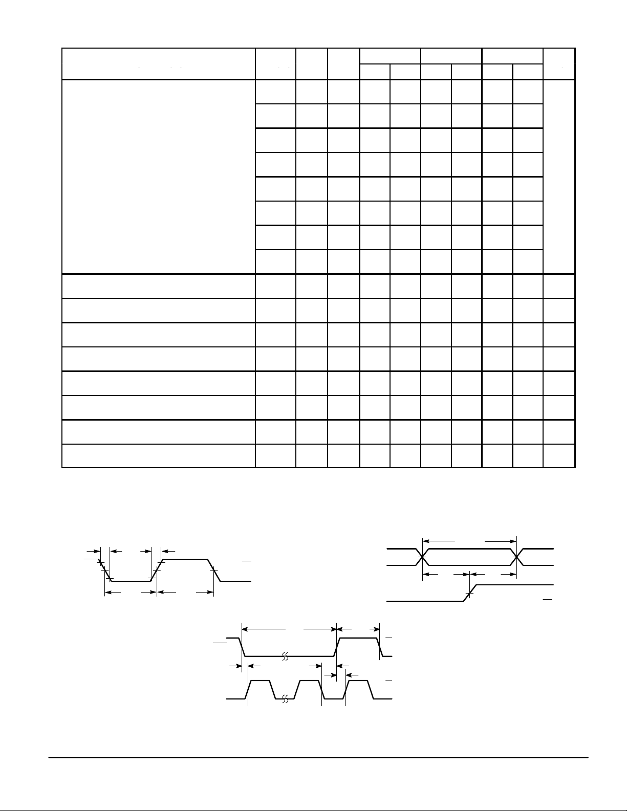
ELECTRICAL CHARACTERISTICS (Continued)
V
DD
V
LCD
40°C 25°C 85°C
Characteristic Symbol
Output Drive Current — Backplanes VO = 2.65 V IBH*
VO = 0.15 V I
VO = 1.08V I
VO = 1.72 V I
VO = 5.35 V I
VO = 0.15 V I
VO = 1.98 V I
VO = 3.52 V I
Pulse Width, Data Clock (Figure 1) t
DCLK Rise/Fall Time (Figure 1) tr, t
Setup Time, Din to DCLK (Figure 2) t
Hold Time, Din to DCLK (Figure 2) t
DCLK Low to ENB High (Figure 3) t
ENB High to DCLK High (Figure 3) t
ENB High Pulse Width (Figure 3) t
ENB Low to DCLK High (Figure 3) t
NOTE: Timing for Figures 1, 2, and 3 are design estimates only.
* For a time (t = 4/OSC FREQ.) after the backplane waveform changes to a new voltage level, the circuit is maintained in the high–current state
to allow the load capacitances to charge quickly. The circuit is then returned to the low–current state until the next voltage change.
I
I
I
I
I
I
I
I
BL
BH
BL
BH
BL
BH
BL
BH
BL
BH
BL
BH
BL
BH
BL
w
su
h
h
rec
w
su
V
5
5
5
5
5
5
5
5
5
5
5
5
5
5
5
5
5
3
5
f
3
5
3
5
3
5
3
5
3
5
3
5
3
V
Min Max Min Max Min Max
2.8
–290
2.8
–290——
2.8
310
2.8
310——
2.8
2.8
2.8
2.8
5.5
5.5
5.5
5.5
5.5
5.5
5.5
5.5
90
—
–90——
–490
–490——
600
600——
100——
–100——–1–35——–1–50——
—
1
–1.5
1.555—
–240
–240——
260
260——
40
—
–40——–1–60——
–520
–520——
600
600——
50
100——
—
—20120
30
60
10
20
10
20
50
100——
10
20
—
2
—
1
0
—
0
—
—
—
—
—
—
—
—
—
–240
–240——
230
230——
55
—
–1
–520
–520——
580
580——
70
—
–1
Unit
µA
—
1
—
1
ns
µs
ns
ns
ns
ns
ns
ns
90%
CLK
50%
10%
MOTOROLA
t
f
t
w
t
r
t
w
Figure 1.
ENB
CLK
SWITCHING WAVEFORMS
V
DD
GND
50%
50%
FIRST
CLK
t
su
t
w
LAST
CLK
Figure 3.
t
w
t
h
t
D
CLK
rec
VALID
in
50%
t
su
50%
t
h
V
DD
GND
V
DD
GND
Figure 2.
V
DD
GND
V
DD
GND
MC145003 • MC145004
3
Page 4
FUNCTIONAL DESCRIPTION
The MC145003/MC145004 has essentially two sections
which operate asynchronously from each other; the data input
and storage section and the LCD drive section. The LCD drive
and timing is derived from the oscillator, while the data input
and storage is controlled by the Data In (Din), Data Clock
(DCLK), Address (A0, A1, A2), and Enable (ENB
) pins.
Data is shifted serially into the 128–bit shift register and
arranged into four consecutive blocks of 32 parallel data bits.
A time–multiplex of the four backplane drivers is made (each
backplane driver becoming active then inactive one after
another) and, at the start of each backplane active period, the
corresponding block of 32 bits is made available at the frontplane drivers. A high input to a plane driver turns the driver on,
and a low input turns the driver off.
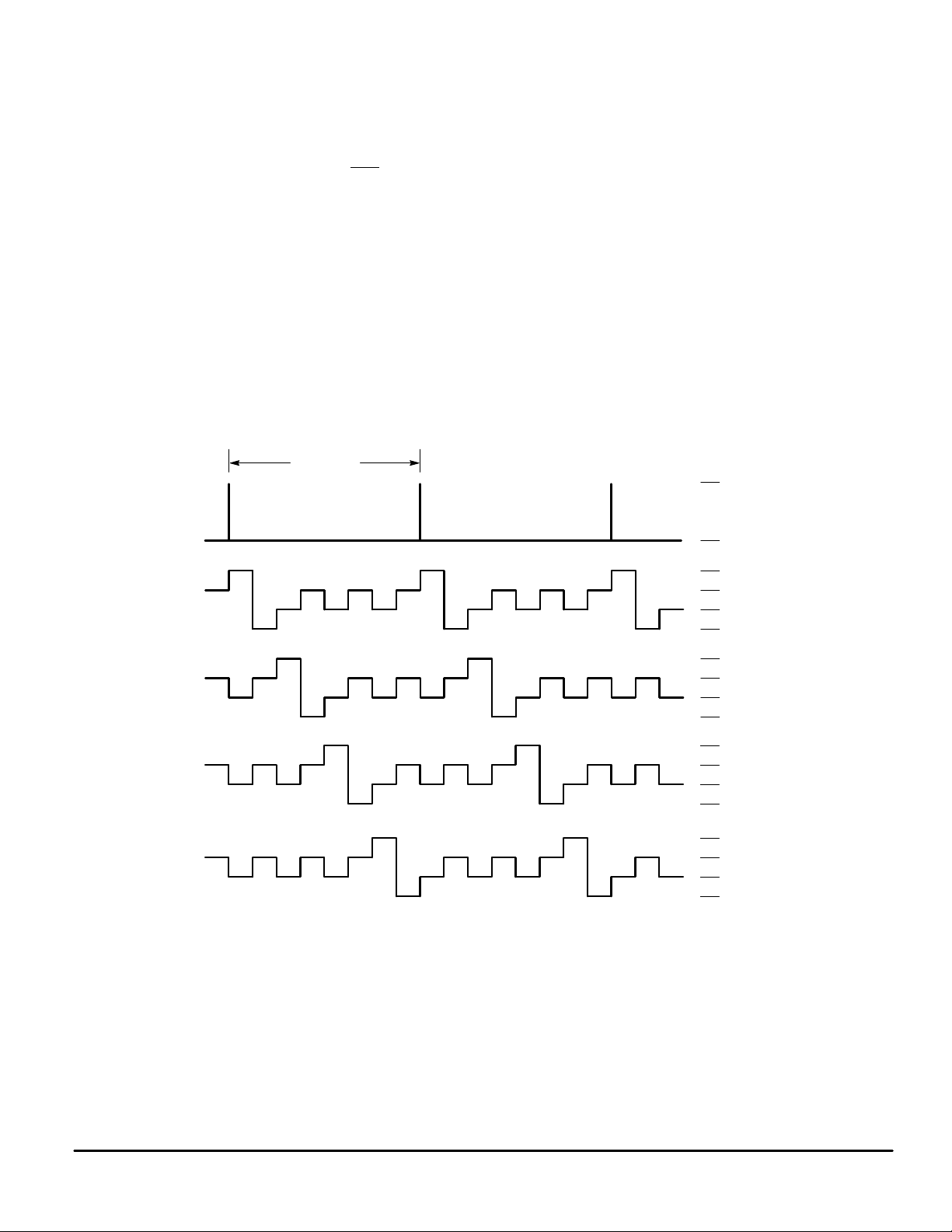
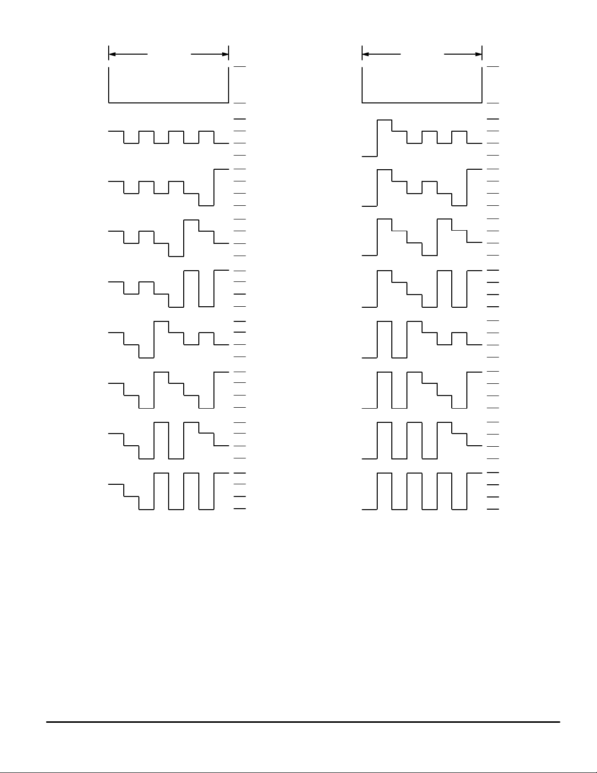
Figure 4 shows the sequence of backplanes. Figure 5
shows the possible configurations of the frontplanes relative
to the backplanes. When a backplane driver is on, its output
switches from V
FRAME
SYNC
PULSE
to 0 V , and when it is off, it switches from
LCD
TIME FRAME
1/3 V
output switches from 0 V to V
from 2/3 V
LCD
to 2/3 V
to 1/3 V
LCD
. When a frontplane driver is on, its
LCD
LCD
, and when it is off, it switches
LCD
.
The LCD drive and timing section provides the multiplex signals and backplane driver input signals and formats the frontplane and backplane waveforms. It also provides a “frame
sync” pulse which may be used in a system where many LCD
drivers are cascaded, to synchronize the backplanes/frontplanes of all participating LCD drivers.
The address pins are used in cascaded systems to uniquely
distinguish one LCD driver from another (and from any other
chips on the same bus) and to define one LCD driver as the
“master” in the system. There must be one master in any
system.
The enable pin may be used as a third control line in the
communication bus. It may be used to define the moment
when the data is latched. If not used, then the data is latched
after 128 bits of data have been received.
V
LCD
0 V
BP1
BP2
BP3
BP4
Figure 4. Backplane Sequence
V
LCD
2/3 (V
1/3 (V
0 V
V
LCD
2/3 (V
1/3 (V
0 V
V
LCD
2/3 (V
1/3 (V
0 V
V
LCD
2/3 (V
1/3 (V
0 V
LCD
LCD
LCD
LCD
LCD
LCD
LCD
LCD
)
)
)
)
)
)
)
)
MC145003 • MC145004 MOTOROLA
4
Page 5
FRAME
SYNC
PULSE
TIME FRAME
V
0 V
LCD
FRAME
SYNC
PULSE
TIME FRAME
V
0 V
LCD
FP DATA
BITS
4321
0000
1000
0100
1100
0010
1010
0110
1110
V
LCD
2/3 (V
1/3 (V
0 V
V
LCD
2/3 (V
1/3 (V
0 V
V
LCD
2/3 (V
1/3 (V
0 V
V
LCD
2/3 (V
1/3 (V
0 V
V
LCD
2/3 (V
1/3 (V
0 V
V
LCD
2/3 (V
1/3 (V
0 V
V
LCD
2/3 (V
1/3 (V
0 V
V
LCD
2/3 (V
1/3 (V
0 V
LCD
LCD
LCD
LCD
LCD
LCD
LCD
LCD
LCD
LCD
LCD
LCD
LCD
LCD
LCD
LCD
V
)
)
)
)
)
)
)
)
)
)
)
)
)
)
)
)
FP DATA
BITS
4321
0001
1001
0101
1101
0011
1011
0111
1111
LCD
2/3 (V
1/3 (V
0 V
V
LCD
2/3 (V
1/3 (V
0 V
V
LCD
2/3 (V
1/3 (V
0 V
V
LCD
2/3 (V
1/3 (V
0 V
V
LCD
2/3 (V
1/3 (V
0 V
V
LCD
2/3 (V
1/3 (V
0 V
V
LCD
2/3 (V
1/3 (V
0 V
V
LCD
2/3 (V
1/3 (V
0 V
LCD
LCD
LCD
LCD
LCD
LCD
LCD
LCD
LCD
LCD
LCD
LCD
LCD
LCD
LCD
LCD
)
)
)
)
)
)
)
)
)
)
)
)
)
)
)
)
MOTOROLA
Figure 5. Frontplane Combinations
MC145003 • MC145004
5
Page 6

PIN DESCRIPTIONS
A0–A2
Address Inputs (Pins 42–44)
The devices have to receive a correct address before they
will accept data. Three address pins (A2, A1, A0) are used to
define the states of the three programmable bits of
MC145003/MC145004’s 8–bit address.
The address is 0111vwxy where v, w, x represent A2, A1,
and A0 respectively. Where v, w, x = 0, then A2, A1, and A0
should be tied to 0 V. Where v, w, x= 1, then A2, A1, and A0
should be tied to VDD.
For systems where only one MC145003/MC145004 is
used, the address pins must be tied to VDD. This defines the
device as a master. Other configurations of the address pins
(except 000*) defines a device to be a slave. For systems with
more than one MC145003/MC145004 (cascaded application)
one of the MC145003/MC145004 must have all of its address
pins tied to VDD (this defines it as the master). The master is
responsible for:
1. Supplying the oscillator input to all slaves.
2. Sending one frame sync pulse at the beginning of every
BP1 (backplane 1) period to keep the MC145003/
MC145004 synchronized.
3. Supplying a common set of backplane signals to be
shared by all participating devices in the cascaded system (if desired).
NOTE
Note: In applications where the circuit will be isolated from
external manual interference the system designer may take advantage of the self–programming feature. Upon power–on, address pins which are left open–circuit will be charged to VDD.
However, care must be taken not to inadvertently discharge the
pins after power–on since the address may then be lost. A similar feature is also available on the ENB
pin.
CAUTION
The configuration A0, A1, A2 = 000 should not be used. This
does not give a valid address and is reserved for Motorola’s use
only. All three address pins should never be tied to 0 V simultaneously. Any other combination of Master (1 1 1) plus six Slaves
(110, 101, 100, 011, 010, 001) is allowed.
ENB
Enable Input (Pin 41)
If the ENB
pin is tied to VDD, the MC145003/MC145004 will
always latch the data after 128 bits have been received. The
latched data is multiplexed and fed to the frontplane drivers for
display . If external control of this latching function is required
(for example, in a cascaded application where multiplexing
of new data may require a delay until all participating
MC145003/MC145004 data is updated), then the ENB
should be held low, followed by one high pulse on ENB
pin
when
data display is required. (This may also be useful in a system
where one MC145003/MC145004 is permanently addressed
and only the last 128 bits of data sent are required to be
latched for display). The pulse on the ENB
pin must occur
while DCLK is high.
DCLK, D
in
Data Clock and Data Input (Pins 38, 39)
Address input and data input controls. See Data Input
Protocol sections for relevant option.
OSC1, OSC2
Oscillator Pins (Pins 51, 50)
To use the on–board oscillator, an external resistor should
be connected between OSC1 and OSC2 of the master device.
Optionally , the OSC1 pin of the master device may be driven
by an externally generated clock signal. The oscillator signal
for any slave(s) in the system is provided by the master device
by connecting the master’s OSC2 pin to the slaves’(s) OSC2
pin(s). The slaves’(s) OSC1 pin(s) should be connected to
ground.
A resistor of 680 kΩ connected between the master’s OSC1
and OSC2 pins gives an oscillator frequency of about 30 kHz,
giving approximately 30 Hz as seen at the LCD driver outputs.
A resistor of 200 kΩ gives about 100 kHz, which results in
100 Hz at the driver outputs. LCD manufacturers recommend
an LCD drive frequency of between 30 Hz and 100 Hz. See
Figure 6.
10 M
1 M
100 k
EXTERNAL RESISTOR VALUE
10 k
1 k 10 k 100 k 1 M 10 M
OSCILLA TOR FREQUENCY
Figure 6. Oscillator Frequency vs Load Resistance
(Approximate)
FS
Frame Sync (Pin 37)
The frame sync pin (FS) is configured as an output on the
master device and as an input on the slave device(s). The
master device outputs a pulse on the FS pin once at the beginning of each BP1 (backplane 1) active period to keep all
MC145003/MC145004s synchronized.
FP1–FP32
Frontplane Drivers (Pins 36–27, 25–22, 19–15, 13–1)
Frontplane driver outputs.
BP1–BP4
Backplane Drivers (Pins 48–45)
Backplane driver outputs.
V
LCD
LCD Driver Supply (Pin 20)
Power supply input for LCD drive outputs. May be used to
supply a temperature–compensated voltage to the LCD drive
section, which can be separate from the logic voltage supply ,
VDD.
MC145003 • MC145004 MOTOROLA
6
Page 7

V
DD
Positive Power Supply (Pin 49)
This pin supplies power to the main processor interface and
logic portions of the device. The voltage range is 2.8 to 5.5 V
with respect to the VSS pin.
For optimum performance, VDD should be bypassed to
VSS using a low inductance capacitor mounted very closely to
these pins. Lead length on this capacitor should be minimized.
V
SS
Ground (Pin 21)
Common ground.
DATA INPUT PROTOCOL
Two–wire communication bus DCLK, Din; three–wire communication bus DCLK, Din, ENB
MC145003 — SPI DEVICE (FIGURE 7)
Before communication with an MC145003 can begin, a start
condition must be set up on the bus by the transmitter. To
establish a start condition, the transmitter must pull the data
line low while the clock line is high. The “idle” state for the
clock line and data line is the high state.
After the start condition has been established, an eight–bit
address should be sent by the transmitter. If the address sent
corresponds to the address of (one of) the MC145003(s) then
on each successive clock pulse, the addressed device will
accept a data bit.
If the ENB
MC145003’s internal counter latches the data to be displayed
after 128 data bits have been received. Otherwise, the control
of this latch function may be overridden by holding the ENB
line low until the new data is required to be displayed, then a
high pulse should be sent on the ENB
must be sent during DCLK high (clock idle).
T o end communication with an MC145003, a stop condition
should be set up on the bus (or another start condition may be
set up if another communication is desired). Note that the
communication channel to an addressed device may be left
open after the 128 data bits have been sent by not setting up
a stop or a start condition. In such a case, the 129th rising
DCLK edge, which normally would be used to set up the stop
or start condition, is ignored by the MC145003 and data continues to be received on the 130th rising DCLK. The latch function continues to work as normal (i.e., data is be latched either
after each block of 128 data bits has been received or under
external control as required).
At any time during data transmission, the transfer may be
interrupted with a stop condition. Data transmission may be
resumed with a start condition and resending the address.
Interfacing the MC145003 with the MC6805 family
The MC145003 performs as a slave receiver in an SPI environment if the clock idle state has been defined to be “high”
(SPICR5 = 1). In three–wire or four–wire SPI environments,
the slave select wire (SPISS) can be used for the ENB
the MC145003 as described above. Note that in full duplex
SPI environments, MC145003 only receives data, it does not
re–transmit data.
MC145004 — IIC DEVICE (FIGURE 8)
Before communication with an MC145004 can begin, a start
condition must be set up on the bus by the controller. To establish a start condition, the controller must pull the data line low
while the clock line is high.
pin is permanently high, then the addressed
.
line. The high pulse
pin on
After the start condition has been established, an eight–bit
address should be sent by the controller followed by an extra
clock pulse while the data line is left high. In this option, only
the seven most significant bits of the address are used to
uniquely define devices on the bus, the least significant bit is
used as a read/write control: if the least significant bit is 0, then
the controller writes to the LCD driver; if it is 1, then the controller reads from the LCD driver’s 128–bit shift register on a
first–in first–out basis. If the seven most significant address
bits sent correspond to the address of (one of) the LCD driver(s) then the addressed LCD driver responds by sending an
“acknowledge” bit back to the controller (i.e., the LCD driver
pulls the data line low during the extra clock pulse supplied by
the controller). If the least significant address bit was 0, then
the controller should continue to send data to the LCD driver
in blocks of eight bits followed by an extra ninth clock pulse to
allow the LCD driver to pull the data line Din low as an acknowledgement. If the least significant address bit was 1, then the
LCD driver sends data back to the controller (the clock is supplied by the controller). After each successive group of eight
bits sent, the LCD driver leaves the data line high for one
pulse.
If the ENB
MC145004’s internal counter latches the data to be displayed
after 128 data bits have been received. Otherwise the control
of this latch function may be overridden by holding the ENB
line low until the new data is required to be displayed, then a
high pulse should be sent on the ENB
must be sent during DCLK high (clock idle).
T o end communication with an MC145004, a stop condition
should be set up on the bus (or another start condition may be
set up if another communication is desired). Note that the
communication channel to an addressed device may be left
open after the 128 data bits have been sent by not setting up
a stop or a start condition. In such a case the rising DCLK edge
which comes after all 128 data bits have been sent and after
the last acknowledge–related clock pulse has been made is
ignored; data continues to be received on the following DCLK
high. The latch function continues to work as normal (i.e., data
is latched either after each block of 128 data bits has been received or under external control as required).
At any time during data transmission, the transfer may be
interrupted with a stop condition. Data transmission may be
resumed with a start condition and resending the address.
CASCADED OPERATION
The master device supplies the oscillator input via its OSC2
pin to the slave devices via their OSC2 pin(s). It sends a frame
sync pulse via its FS pin to the slaves via their FS pins at the
beginning of every BP1 valid time. In Figure 9, the ENB
are tied together and used as a chip enable to latch the new
data — the ENB
sirable to use the internal data bit counter to latch the new
data.
The four backplane inputs may come from the master only ,
with the slave backplanes being left open, as shown in Figure
6, or if more drive is required, then the slaves’ backplanes may
be connected to the corresponding backplanes of the master.
Example: at room temperature, with a drive frequency of 30
Hz, around four to five MC145003/MC145004s may be used
in a system where only the master’s backplanes are connected to the LCD. For applications with heavier loads (e.g.,
large liquid crystals) or high drive frequencies or at high temperatures, the dc voltage component seen by the LCD may be
kept to a minimum by connecting the corresponding backplanes of all participating MC145003/MC145004s together.
pin is permanently high, then the addressed
line. The high pulse
pins
pins could have been tied to VDD if it were de-
MOTOROLA
MC145003 • MC145004
7
Page 8

129TH DCLK HIGH:
(DOES NOT SHIFT DATA)
STAR T
BUT MUST BE DURING DCLK HIGH.
ENABLE PULSE MAY OCCUR AS REQUIRED;
4321
•
•
•
A2 A1 A0 BP4 BP3 BP2 BP1 BP4 BP3 BP2 BP1
in
D
FP1 FP2
DCLK
Figure 7a. Data Input — MC145003
Figure 7b. Serial 128 Bits Data
FP1 FP2 FP3 FP4 FP5 FP6 FP32
(BPi, FPj) ON
x
4 32 143214321432143214321
in
BP
D
STAR T 8-BITS ADDRESS 128-BITS DAT A
ENB
(IF USED)
(BPi, FPj) OFF
→
→
0
x: 1
Figure 7. MC145003 (SPI DEVICE)
MC145003 • MC145004 MOTOROLA
8
Page 9

LAST DCLK PULSE
(DOES NOT SHIFT DATA)
BUT MUST BE DURING DCLK HIGH.
ENABLE PULSE MAY OCCUR AS REQUIRED;
LAST DCLK PULSE
(DOES NOT SHIFT DATA)
ACKNOWLEDGE
ENTIRE CLK FOR
STOP
LEFT HIGH BY DRIVER
LEFT HIGH
BY CONTROLLER
FP1 FP2
LEFT HIGH
BY CONTROLLER
ACKNOWLEDGE
ENTIRE CLK FOR
ACKNOWLEDGE
ENTIRE CLK FOR
CONTINUES TO CLOCK DATA AND ACKNOWLEDGE
PULLED LOW BY DRIVER STOP
PULLED LOW BY DRIVER
ACKNOWLEDGE
ENTIRE CLK FOR
ACKNOWLEDGE
ENTIRE CLK FOR
CONTINUES TO CLOCK DATA AND ACKNOWLEDGE
ADDRESS ACKNOWLEDGED BY DRIVER LEFT HIGH BY DRIVER
(LOW-ORDER BIT = 0)
D
WRITE TO LCD DRIVER
MOTOROLA
A2 A1 A0 BP4 BP3 BP2 BP1 BP4 BP3 BP2 BP1
in
(FROM
CONTROLLER)
DCLK
(LOW-ORDER BIT = 1)
STAR T 8-BITS ADDRESS 8-BITS DAT A
in
D
DRIVER)
(FROM LCD
ENB
(IF USED)
READ FROM LCD DRIVER
D
Figure 8. Data Input MC145004 (IIC Device)
in
(FROM
CONTROLLER)
STAR T 8-BITS ADDRESS 8-BITS DAT A
DCLK
in
D
DRIVER)
(FROM LCD
MC145003 • MC145004
9
Page 10

Ω
BP1–BP4
680 k
TO
OTHER
CHIPS
ON BUS
LIQUID CRYST AL DISPLAY
FP1–FP32 BP1–BP4FP33–FP64
FP1–FP32
FP32
FP31
FP30
FP29
FP28
FP27
FP26
FP25
FP24
FP23
FP22
FP21
FP20
OSC1
OSC2
FP19
V
FP18
DD
BP1
FP17
FP16
BP2
BP3
BP4
(MASTER)
LCD DRIVER
LCD
SS
FP15VV
A0A1A2
FP14
FP13
FP12
ENB
DCLK
FP10
FP11
D
in
FS
FP1
FP2
FP3
FP4
FP5
FP6
FP7
FP8
FP9
FP32
FP31
FP1–FP32
FP30
FP29
FP28
FP27
FP26
FP25
FP24
FP23
FP22
FP21
FP20
OSC1
OSC2
FP19
V
FP18
DD
BP1
FP17
BP2
FP16
FP15VV
A0A1A2
BP3
BP4
(SLAVE)
LCD DRIVER
LCD
SS
FP14
CONTROLLER
FP13
FP12
ENB
FP11
Figure 9. Cascading Example
D
in
DCLK
FS
FP1
FP2
FP3
FP4
FP5
FP6
FP7
FP8
FP9
FP10
SS
DATA
CLOCK
V
DD
LCD
V
V
SS
MC145003 • MC145004 MOTOROLA
10
Page 11

APPLICATION INFORMATION
Figure 10 shows an interface example.
Example 1 shows a semi–automatic SPI Mode (only start and stop conditions are done in non–SPI Mode). Example 2 contains
the software to use HC1 1 with MC145003 in manual SPI Mode. Both examples use the same hardware connection.
V
DD
OSC1
OSC2
FP1–FP32
R = 470 k
MC68HC11
V
DD
1 k
Ω
A0
A1 A2
MOSI
SCK
SS
1/4 MUX DISPLAY
D
DCLK
ENB
BP1–BP4
in
MC145003
Figure 10. Interface Example Between MC68HC11 and MC145003
Ω
CPOL = 0
CPHA = 0
SPI Off
EW
= 0
Setup Start Condition with SPI off (Write Data Port to 0)
SPI On < ldaa $73, staa $1028
Send Address Byte $7E
Send 16 bytes of Data
SPI Off < ldaa $33, staa $1028
DATA = 0 SPI Off
ENB
= 1
CLK = 1
DATA = 1 Stop Condition
Allows the latch of data to the FP outputs
Example 1. Semi–Automatic SPI Method
MOTOROLA
MC145003 • MC145004
11
Page 12

1
2 ;=======CONSTANTS=================================================
3 0000 T extram equ $A000 ;$A000 for 8K RAM
4 0000 T stack equ $00FF ;last RAM byte
5 0000 T intofs equ $1000 ;Internal Registers
6 0000 T data equ $08
7 0000 T clock equ $10
8 0000 T enable equ $20
9 0000 T portd equ 8
10
11
12 ;=======PROGRAM BEGIN=============================================
13 A000 T org extram ;Program into RAM
14 A000 N 8E00FF cold lds #stack ;set stack pointer
15 A003 M 8638 ldaa #$38 ;set of MOSI,SS,SCK
16 A005 T B71009 staa $1009 ;DDRD
17 A008 M C611 ldab #17
18 A00A N CEA05E ldx #send
19 A00D T BDA010 jsr spi
20 A010 T end cold
21
22 A010 U 18CE1000 spi ldy #intofs
23 A014 J 181D0820 bclr portd,y #enable ;EN = 0
24 A018 T BDA031 jsr start ;start condition
25 A01B X A600 again ldaa 0 , x ;SPI Mode Use
26 A01D T B7102A staa $102A ;SPDR
27 A020 L 181F2980FB brclr $29,y,#$80,*
28 A025 H 08 inx ;next DATA
29 A026 H 5A decb
30 A027 R 26F2 bne again
31 A029 J 181C0820 bset portd,y #enable
32 A02D T BDA04C jsr stop ;stop condition
33 A030 H 39 rts
34
35 A031 M 8633 start ldaa #$33 ;Normal Mode
36 A033 T B71028 staa $1028 ;SPCR
37 A036 J 181C0808 bset portd,y #data ;DATA = 1
38 A03A J 181C0810 bset portd,y #clock ;CLK = 1
39 A03E J 181D0808 bclr portd,y #data ;DATA = 0
40 A042 J 181D0810 bclr portd,y #clock ;CLK = 0
41 A046 M 8673 ldaa #$73 ;SPI Mode
42 A048 T B71028 staa $1028 ;SPCR
43 A04B H 39 rts
44 A04C M 8633 stop ldaa #$33 ;Normal Mode
45 A04E T B71028 staa $1028 ;SPCR
46 A051 J 181D0808 bclr portd,y #data ;DATA = 0
47 A055 J 181C0810 bset portd,y #clock ;CLK = 1
48 A059 J 181C0808 bset portd,y #data ;DATA = 0
49 A05D H 39 rts
50
51 A05E T 7E send fcb $007E ;LCD Driver Address
52 A05F T F0 fcb $00f0 ;Data to sent
53 A060 T F0 fcb $00f0
54 A061 T F0 fcb $00f0
55 A062 T F0 fcb $00f0
56 A063 T F0 fcb $00f0
57 A064 T F0 fcb $00f0
58 A065 T F0 fcb $00f0
59 A066 T F0 fcb $00f0
60 A067 T F0 fcb $00f0
61 A068 T F0 fcb $00f0
62 A069 T F0 fcb $00f0
63 A06A T F0 fcb $00f0
64 A06B T F0 fcb $00f0
65 A06C T F0 fcb $00f0
66 A06D T F0 fcb $00f0
67 A06E T F0 fcb $00f0
68 A06F H 39 rts
69
70 ;=======PROGRAM END===============================================
Example 2. Manual Method
MC145003 • MC145004 MOTOROLA
12
Page 13

P ACKAGE DIMENSIONS
QFP
FU SUFFIX
CASE 848B–02
L
39
40
-A-
L
DETAIL A
52
27
26
S S
S S
-D-
B
14
V
M
0.20 (0.008) H A–B D
0.05 (0.002) A–B
M
0.20 (0.008) C A–B D
B
1
-D-
13
B
B
0.20 (0.008) A–B D
0.05 (0.002)
M
A–B
V
0.20 (0.008) A–B D
M
S S
H
-A,B,D-
DETAIL A
S S
C
F
C
M
E
DETAIL C
J
N
-C-
SEATING
PLANE
DATUM
PLANE
-H-
DATUM
-H-
PLANE
H
G
M
0.10 (0.004)
D
0.02 (0.008) A–B D
M
C
BASE METAL
S S
SECTION B-B
MILLIMETERS INCHES
MIN MINMAX MAX
DIM
A
B
C
D
E
F
G
H
J
K
L
M
N
Q
R
S
T
U
V
W
X
9.90
9.90
2.10
0.22
2.00
0.22
0.65 BSC
—
0.13
0.65
7.80 REF
°
5
0.13
°
0
0.13
12.95
0.13
°
0
12.95
0.35
1.6 REF
10.10
10.10
2.45
0. 38
2.10
0.33
0.25
0.23
0.95
°
10
0.17
°
7
0.30
13.45
—
—
13.45
0.45
0.390
0.390
0.083
0.009
0.079
0.009
0.026 BSC
—
0.005
0.026
0.307 REF
°
5
0.005
°
0
0.005
0.510
0.005
°
0
0.510
0.014
0.063 REF
0.398
0.398
0.096
0.015
0.083
0.013
0.010
0.009
0.037
10
0.007
°
7
0.012
0.530
—
—
0.530
0.018
°
DETAIL C
U
T
R
K
W
X
NOTES:
1. DIMENSIONING AND TOLERANCING PER ANSI
Y14.5M, 1982.
2. CONTROLLING DIMENSION: MILLIMETER.
3. DATUM PLANE –H– IS LOCATED AT BOTTOM OF
LEAD AND IS COINCIDENT WITH THE LEAD WHERE
THE LEAD EXITS THE PLASTIC BODY AT THE
BOTTOM OF THE PARTING LINE.
4. DATUMS –A–, –B– AND –D– TO BE DETERMINED AT
DATUM PLANE –H–.
Q
5. DIMENSIONS S AND V TO BE DETERMINED AT
SEATING PLANE –C–.
6. DIMENSIONS A AND B DO NOT INCLUDE MOLD
PROTRUSION. ALLOWABLE PROTRUSION IS 0.25
(0.010) PER SIDE. DIMENSIONS A AND B DO
INCLUDE MOLD MISMATCH AND ARE DETERMINED
AT DATUM PLANE –H–.
7. DIMENSION D DOES NOT INCLUDE DAMBAR
PROTRUSION. ALLOWABLE DAMBAR PROTRUSION
SHALL BE 0.08 (0.003) TOTAL IN EXCESS OF THE D
DIMENSION AT MAXIMUM MATERIAL CONDITION.
DAMBAR CANNOT BE LOCATED ON THE LOWER
RADIUS OR THE FOOT.
MOTOROLA
MC145003 • MC145004
13
Page 14

Motorola reserves the right to make changes without further notice to any products herein. Motorola makes no warranty , representation or guarantee regarding
the suitability of its products for any particular purpose, nor does Motorola assume any liability arising out of the application or use of any product or circuit,
and specifically disclaims any and all liability, including without limitation consequential or incidental damages. “T ypical” parameters can and do vary in different
applications. All operating parameters, including “T ypicals” must be validated for each customer application by customer’s technical experts. Motorola does
not convey any license under its patent rights nor the rights of others. Motorola products are not designed, intended, or authorized for use as components in
systems intended for surgical implant into the body, or other applications intended to support or sustain life, or for any other application in which the failure of
the Motorola product could create a situation where personal injury or death may occur. Should Buyer purchase or use Motorola products for any such
unintended or unauthorized application, Buyer shall indemnify and hold Motorola and its officers, employees, subsidiaries, affiliates, and distributors harmless
against all claims, costs, damages, and expenses, and reasonable attorney fees arising out of, directly or indirectly, any claim of personal injury or death
associated with such unintended or unauthorized use, even if such claim alleges that Motorola was negligent regarding the design or manufacture of the part.
Motorola and are registered trademarks of Motorola, Inc. Motorola, Inc. is an Equal Opportunity/Affirmative Action Employer.
Literature Distribution Centers:
USA: Motorola Literature Distribution; P.O. Box 20912; Phoenix, Arizona 85036.
EUROPE: Motorola Ltd.; European Literature Centre; 88 T anners Drive, Blakelands, Milton Keynes, MK14 5BP, England.
JAPAN: Nippon Motorola Ltd.; 4–32–1, Nishi–Gotanda, Shinagawa–ku, Tokyo 141, Japan.
ASIA PACIFIC: Motorola Semiconductors H.K. Ltd.; Silicon Harbour Center , No. 2 Dai King Street, T ai Po Industrial Estate, Tai Po, N.T., Hong Kong.
CODELINE TO BE PLACED HERE
MC145003 • MC145004 MOTOROLA
14
◊
*MC145003/D*
MC145003/D
 Loading...