

Page 1
MC14497MOTOROLA
1
The M C14497 is a P CM remote c ontrol transmitter realized in C MOS
technology. Using a dual–single (FSK/AM) frequency bi–phase modulation, the
transmitter is designed to work with the MC3373 receiver. Information on the
MC3373 can be found in the Motorola
Linear
and
Interface Integrated Circuits
book (DL128/D).
There is not a d ecoder device w hich is compatible with the MC14497.
Typically, the decoding resides in MCU software.
• Both FSK/AM Modulation Selectable
• 62 Channels (Up to 62 Keys)
• Reference Oscillator Controlled by Inexpensive Ceramic Resonator:
Maximum Frequency = 500 kHz
• Very Low Duty Cycle
• Very Low Standby Current: 50 µA Maximum
• Infrared Transmission
• Selectable Start–Bit Polarity (AM Only)
• Shifted Key Mode Available
• Wide Operating Voltage Range: 4 to 10 V
• See Application Notes AN1016 and AN1203
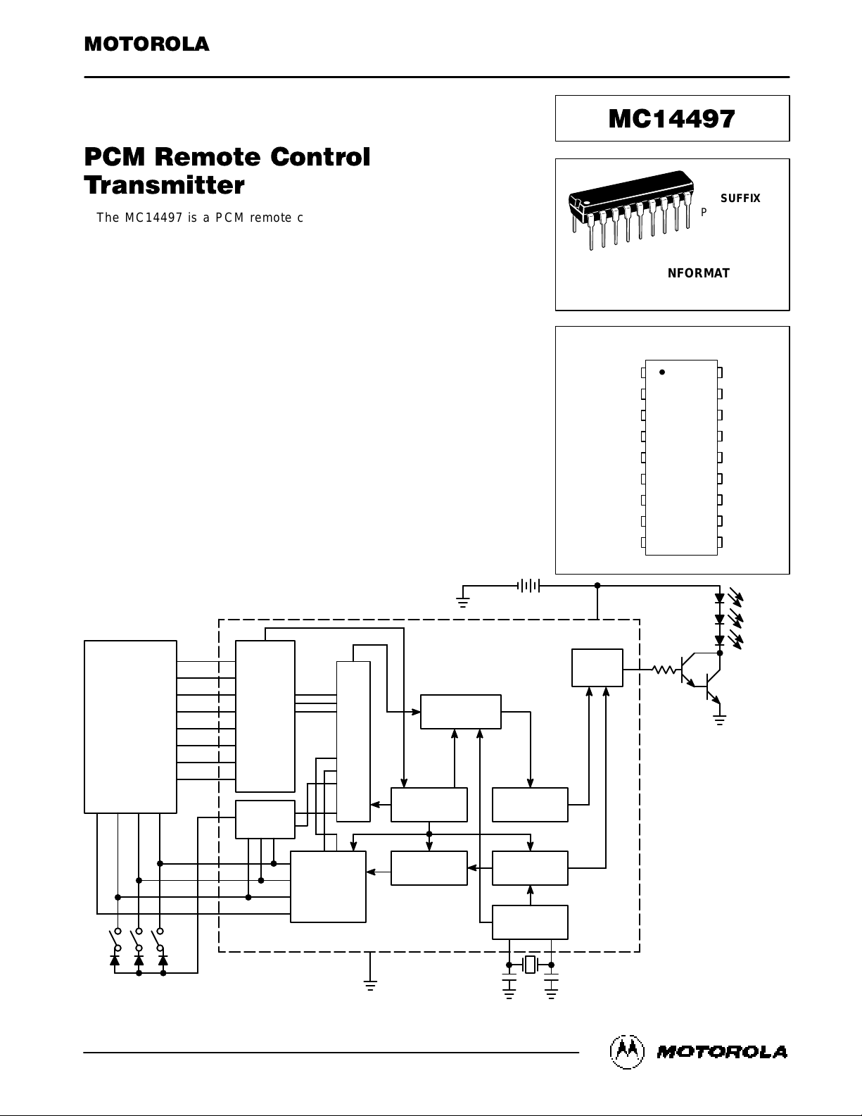
BLOCK DIAGRAM
17
E1
2
E2
1
E3
16
E4
15
E5
14
E6
10
E7
11
E8
ENCODER
7–BIT
SR
SEQUENCE
CONTROL
3–BIT
LATCH
OUTPUT
CONTROL
DIVIDER
÷
10/12
MUX
SCANNER
DIVIDER
÷
32
DIVIDER
÷
16
OSC
STANDBY
7
6
5
4
FK3
E9
3
FK1
A4 A3 A2 A1
9
V
DD
18
8
IN OUT
12 13
500 kHz CERAMIC
RESONATOR
KEYBOARD
Order this document
by MC14497/D
SEMICONDUCTOR TECHNICAL DATA
P SUFFIX
PLASTIC DIP
CASE 707
ORDERING INFORMATION
MC14497P Plastic DIP
PIN ASSIGNMENT
A3
E9
E2
E3
V
SS
SIGNAL OUT
A1
A2
A4 E5
E4
E1
V
DD
E7
E8
OSC
in
OSC
out
E614
15
16
17
18
10
11
12
13
5
4
3
2
1
9
8
7
6
18
1
Motorola, Inc. 1995
SAME AS IN DL136/D R3
Page 2

MC14497 MOTOROLA
2
MAXIMUM RATINGS (Voltages referenced to V
SS
)
Parameter
Symbol
Value
Unit
DC Supply Voltage V
DD
– 0.5 to + 18 V
Input Voltage, All Inputs V
in
– 0.5 to VDD + 0.5 V
DC Current Drain per Pin I 10 mA
Operating Temperature Range T
A
– 40 to + 85 °C
Storage Temperature Range T
stg
– 65 to + 150 °C
ELECTRICAL CHARACTERISTICS (T
A
= 0 to 70°C; all Voltages Referenced to VSS)
Characteristic
Symbol V
DD
Min Max Unit
Supply Voltage V
DD
— 4.0 10.0 V
Supply Current
Idle
Operation
I
DD
10
10
—
—
50
5
µA
mA
Output Current — Signal
VOH = 3.0 V Source
VOL = 0.5 V Sink
I
OH
I
OL
4
4
– 900
120
—
—
µA
Output Current — Scanner
VOH = 3.0 V Source
VOL = 0.5 V Sink
I
OH
I
OL
4
4
– 30
245
—
—
µA
Output Current — Oscillator
VOH = 3.0 V Source
VOL = 0.5 V Sink
I
OH
I
OL
4
4
– 300
245
—
—
µA
Input Current — Oscillator
Operation
Idle, VIL = 0.5 V
I
in
10
4
± 2
30
± 80
—
µA
Input Current — Encoder
VIH = 9.0 V
VIL = 0.5 V
I
in
10
4
– 15
—
—
– 60
µA
Input Voltage — Encoder V
IH
V
IL
V
IH
V
IL
10
10
4
4
9
—
3
—
—
1.2
—
1.0
V
This device contains circuitry to protect the
inputs against damage due to high static
voltages or electric fields; however, it is advised that normal precautions be taken to avoid
application of any voltage higher than maximum rated voltages to this high–impedance
circuit. For proper operation it is recommended
that Vin and V
out
be constrained to the range
VSS ≤ (Vin or V
out
) ≤ VDD.
Page 3

MC14497MOTOROLA
3
CIRCUIT OPERATION
The transmitter sends a 6–bit, labelled A (LSB) to F (MSB),
binary code giving a total of 64 possible combinations or
code words. All of these channels are user selectable, except the last two (where channel 63 is not sent while channel
62 is automatically sent by the transmitter at the end of each
transmission as an “End of Transmission” code).
In either mode, FSK or AM, the transmitted signal is in the
form of a bi–phase pulse code modulation (PCM) signal. The
AM coding is shown in Figure 1.
BIT–n
f
1
f
1
“0”
“1”
Figure 1. AM Coding
AM
In the AM mode, f1 is a train of pulses at the modulating
frequency of 31.25 kHz for a reference frequency of 500 kHz.
In the FSK mode, two modulating frequencies are used as
shown in Figure 2.
BIT–n
f
2
f
3
“0”
“1”
Figure 2. FSK Coding
f
2
f
3
FSK
In this mode, f3 is 50 kHz and f2 is 41.66 kHz for a reference frequency of 500 kHz.
The keyboard can be a simple switch matrix using no external diodes, connected to the four scanner inputs (A1 – A4)
and the eight row input (E1 – E8). Under these conditions,
only the first 32 code words are available since bit–F is always at logical 0. However, a simple 2–pole changeover
switch, in the manner of a typewriter “shift” key (switch FK3 in
the Block Diagram) can be used to change the polarity of
bit–F to give access to the next full set of 32 instructions.
An alternative method of accessing more than 32 instructions is by the use of external diodes between the address
inputs (see Figure 3). These have the effect of producing
“phantom” address inputs by pulling two inputs low at the
same time, which causes bit–F to go high (i.e., to logical 1).
By interconnecting only certain address inputs it is possible
to make an intermediate keyboard with between 32 and 64
keys.
The other two switches in the Block Diagram (FK1 and
FK2) change the modulation mode. Closing FK1 changes
the modulation from FSK to AM and the start–bit polarity.
Closing FK2 changes the start–bit to a logical 0.
The full range of options available is illustrated in Table 1.
Table 1.
Start
Bit
Modulation Bit–F Channels
E9 = Open 1 FSK 0 0 – 31
E9 = A1 (FK1) 1 AM 0 0 – 31
E9 = A2 (FK2) 0 FSK 0
0 – 31*
E9 = A3 (FK3) 1 FSK 1 32 – 61
E9 = A1 • A2 0 AM 0 0 – 31
E9 = A1 • A3 1 AM 1 32 – 61
E9 = A2 • A3 0 FSK 1
32 – 61*
E9 = A1 • A2 • A3 0 AM 1 32 – 61
*Not allowed.
One of the transmitter’s major features is its low power
consumption (in the order of 10 µA in the idle state). For this
reason, the battery is perpetually in circuit. It has in fact been
found that a light discharge current is beneficial to battery
life.
In its active state, the transmitter efficiency is increased by
the use of a low duty cycle which is less than 2.5% for the
modulating pulse trains.
While no key is pressed, the circuit is in its idle state and
the reference oscillator is stopped. Also, the eight address input lines are held high through internal pull–up resistors.
As soon as a key is pressed, this takes the appropriate address line low, signaling to the circuit that a key has been selected. The oscillator is now enabled. If the key is released
before the code word has been sent, the circuit returns to its
idle state. T o account for accidental activation of the transmitter, the circuit has a built–in reactive time of approximately
20 ms, which also overcomes contact bounce. After this
delay, the code word will be sent and repeated at 90 ms intervals for as long as the key is pressed. As soon as the key is
released, the circuit automatically sends channel 62, the
“End of Transmission” (EOT) code. The transmitter then returns to its idle state.
The differences between the two modulation modes are illustrated in Figure 4. However, it should be noted that in the
AM mode, each transmitted word is preceded by a burst of
pulses lasting 512 µs. This is used to set up the AGC loop in
the receiver’s preamp. In the FSK mode, the first frequency
of the first bit is extended by 1.5 ms and the AGC burst is
suppressed. In either mode, it is assumed that the normal
start–bit is present.
Page 4

MC14497 MOTOROLA
4
PIN DESCRIPTIONS
E1 – E8
Row Inputs (Pins 1, 2, 10, 11, 14, 15, 16, 17)
Under idle conditions, these inputs are held high by internal pull–up resistors. As soon as a key is pressed, a logical 0
on that particular line signals to the circuit that a key has
been selected. After a delay of 20 ms, the internal register is
loaded with the code word for the key selected.
E9
Row Input (Pin 3)
This is a special programming input and when connected
to the appropriate scanner output via a diode, it will modify
the transmitted output according to Table NO TAG.
In Table NO TAG, the figures in brackets (FK1, etc.) refer
to the switches shown in the Block Diagram and Figure 3. If
only one option is required, the diode may be omitted. The
connections shown in Table NO TAG may be made in any
combination.
Although E9 is a row input, forcing this line low will not activate the circuit.
A1 – A4
Scanner Outputs (Pins 4 – 7)
Under idle conditions, these outputs are held low, logical 0.
When a key is pressed, the circuit is activated and the oscillator will start and release the outputs (see Figure 5).
OSCin, OSC
out
Oscillator Input and Oscillator Output (Pins 12, 13)
These pins are designed to operate with a 500 kHz ceramic resonator or a tune LC circuit. It is important that a ceramic
resonator and not a filter be used here, as the oscillator frequency cannot be guaranteed if a ceramic filter is used.
SIGNAL OUT
Signal Output (Pin 8)
This output provides the modulating signal ready to drive
the modulation amplifier. If required, the transmitter can be
used as a keyboard encoder for direct use with a receiver. In
this case, the AM option is selected, the output inverted, and
fed directly to the receiver’s signal input pin.
Figure 3. 64–Key Keyboard
E1a
E1
E2a
E2
E3a
E3
E4a
E4
E5a
E5
E6a
E6
E7a
E7
E8a
E8
17
2
1
16
15
14
10
11
9 18
V
SS
V
DD
3 13
12
A1
7
A2
6
A3
5
A4
4
FK2 FK1
E9
C1 C2
NOTE: Maximum key contact
resistance = 1 kΩ.
Figure 4. Transmitted Waveforms and Timing (Not Drawn to Scale)
START BIT A B C D E F
f2 f3f3f2f3f2f3f2f3
f1 f1 f1 f1f1 f1
INSTRUCTION
FSK
AM
ONE WORD
DEBOUNCE
KEY WORD
20 ms
9 ms
99 ms
Page 5

MC14497MOTOROLA
5
Figure 5. Scanner Output Timing Diagram
A1
A2
A3
A4
KEY RELEASEDKEY DOWN
DEBOUNCE
Figure 6. Typical Application Circuit
KEYBOARD
9 12 13
1 k
Ω
100
Ω
18
8
100
Ω
0.1
Ω
C1 C2
1500 µF 9 V
1N4001
MC14497
*
*Visible Indicator
C1 and C2 are sized per the ceramic resonator supplier’s recommendation.
Ceramic Resonator Suppliers:
1. Morgan Matrox, Inc., Bedford, OH, 216/232–8600
2. Radio Materials Co., Attica, IN, 317/762–2491
Motorola cannot recommend one supplier over another and in no way suggests that this is a
complete listing of ceramic resonator suppliers.
Page 6

MC14497 MOTOROLA
6
AGC BURST START BIT A B C D E F
f4 f4 f4 f4 f4 f4 f4
540
µ
s
2.84 ms
540
µ
s
1.155 ms 1.1 ms
540
µ
s
590
µ
s
540
µ
s
590
µ
s
540
µ
s
590
µ
s
1.16 ms
540
µ
s
NOTES:
1. f4 = 28.4 kHz.
2. Indicated time durations are approximated.
Figure 7. AM Mode Transmitted Wavetrain with 455 kHz Oscillator
Table 2. Transmitted Codes
Code Word Keyboard Code Word Keyboard
Channel F E D C B A In Out Channel F E D C B A In Out
0 0 0 0 0 0 0 E8 A4 32 1 0 0 0 0 0 E8a A4
1 0 0 1 E1 A4 33 0 0 1 E1a A4
2 0 1 0 E2 A4 34 0 1 0 E2a A4
3 0 1 1 E3 A4 35 0 1 1 E3a A4
4 1 0 0 E4 A4 36 1 0 0 E4a A4
5 1 0 1 E5 A4 37 1 0 1 E5a A4
6 1 1 0 E6 A4 38 1 1 0 E6a A4
7 1 1 1 E7 A4 39 1 1 1 E7a A4
8 0 0 1 0 0 0 E8 A1 40 1 0 1 0 0 0 E8a A1
9 0 0 1 E1 A1 41 0 0 1 E1a A1
10 0 1 0 E2 A1 42 0 1 0 E2a A1
11 0 1 1 E3 A1 43 0 1 1 E3a A1
12 1 0 0 E4 A1 44 1 0 0 E4a A1
13 1 0 1 E5 A1 45 1 0 1 E5a A1
14 1 1 0 E6 A1 46 1 1 0 E6a A1
15 1 1 1 E7 A1 47 1 1 1 E7a A1
16 0 1 0 0 0 0 E8 A3 48 1 1 0 0 0 0 E8a A3
17 0 0 1 E1 A3 49 0 0 1 E1a A3
18 0 1 0 E2 A3 50 0 1 0 E2a A3
19 0 1 1 E3 A3 51 0 1 1 E3a A3
20 1 0 0 E4 A3 52 1 0 0 E4a A3
21 1 0 1 E5 A3 53 1 0 1 E5a A3
22 1 1 0 E6 A3 54 1 1 0 E6a A3
23 1 1 1 E7 A3 55 1 1 1 E7a A3
24 0 1 1 0 0 0 E8 A2 56 1 1 1 0 0 0 E8a A2
25 0 0 1 E1 A2 57 0 0 1 E1a A2
26 0 1 0 E2 A2 58 0 1 0 E2a A2
27 0 1 1 E3 A2 59 0 1 1 E3a A2
28 1 0 0 E4 A2 60 1 0 0 E4a A2
29 1 0 1 E5 A2 61 1 0 1 E5a A2
30 1 1 0 E6 A2 62 1 1 0 E6a A2
31 0 1 1 1 1 1 E7 A2 Not
Transmitted
1 1 1 1 1 1 E7a A2
NOTE: Although the “a” suffix applies to a phantom input when using
a keyboard with up to 64 keys, the coding is identical with a
32–key keyboard when switch FK3 is closed.
Page 7

MC14497MOTOROLA
7
PACKAGE DIMENSIONS
P SUFFIX
PLASTIC DIP
CASE 707–02
MIN MINMAX MAX
MILLIMETERS INCHES
DIM
22.22
6.10
3.56
0.36
1.27
1.02
0.20
2.92
23.24
6.60
4.57
0.56
1.78
1.52
0.30
3.43
0
°
0.51
0.875
0.240
0.140
0.014
0.050
0.040
0.008
0.115
0.915
0.260
0.180
0.022
0.070
0.060
0.012
0.135
15
°
1.02
2.54 BSC
7.62 BSC
0.100 BSC
0.300 BSC
0
°
0.020
15
°
0.040
A
B
C
D
F
G
H
J
K
L
M
N
NOTES:
1. POSITIONAL TOLERANCE OF LEADS (D),
SHALL BE WITHIN 0.25 (0.010) AT MAXIMUM
MATERIAL CONDITION, IN RELATION TO
SEATING PLANE AND EACH OTHER.
2. DIMENSION L TO CENTER OF LEADS WHEN
FORMED PARALLEL.
3. DIMENSION B DOES NOT INCLUDE MOLD
FLASH.
1 9
1018
B
A
H
F
G
D
SEATING
PLANE
N
K
M
J
L
C
Page 8

MC14497 MOTOROLA
8
Motorola reserves the right to make changes without further notice to any products herein. Motorola makes no warranty, representation or guarantee regarding
the suitability of its products for any particular purpose, nor does Motorola assume any liability arising out of the application or use of any product or circuit,
and specifically disclaims any and all liability, including without limitation consequential or incidental damages. “T ypical” parameters can and do vary in different
applications. All operating parameters, including “T ypicals” must be validated for each customer application by customer’s technical experts. Motorola does
not convey any license under its patent rights nor the rights of others. Motorola products are not designed, intended, or authorized for use as components in
systems intended for surgical implant into the body, or other applications intended to support or sustain life, or for any other application in which the failure of
the Motorola product could create a situation where personal injury or death may occur. Should Buyer purchase or use Motorola products for any such
unintended or unauthorized application, Buyer shall indemnify and hold Motorola and its officers, employees, subsidiaries, affiliates, and distributors harmless
against all claims, costs, damages, and expenses, and reasonable attorney fees arising out of, directly or indirectly, any claim of personal injury or death
associated with such unintended or unauthorized use, even if such claim alleges that Motorola was negligent regarding the design or manufacture of the part.
Motorola and are registered trademarks of Motorola, Inc. Motorola, Inc. is an Equal Opportunity/Affirmative Action Employer.
How to reach us:
USA/EUROPE: Motorola Literature Distribution; JAPAN: Nippon Motorola Ltd.; Tatsumi–SPD–JLDC, Toshikatsu Otsuki,
P.O. Box 20912; Phoenix, Arizona 85036. 1–800–441–2447 6F Seibu–Butsuryu–Center, 3–14–2 Tatsumi Koto–Ku, Tokyo 135, Japan. 03–3521–8315
MFAX: RMFAX0@email.sps.mot.com – TOUCHTONE (602) 244–6609 HONG KONG: Motorola Semiconductors H.K. Ltd.; 8B Tai Ping Industrial Park,
INTERNET: http://Design–NET.com 51 Ting Kok Road, Tai Po, N.T., Hong Kong. 852–26629298
MC14497/D
*MC14497/D*
◊
 Loading...