

Datasheet MC14490P, MC14490DW, MC14490DWR2, MC14490FEL, MC14490FL1 Datasheet (MOTOROLA)
...Page 1
Semiconductor Components Industries, LLC, 2000
May, 2000 – Rev. 4
1 Publication Order Number:
MC14490/D
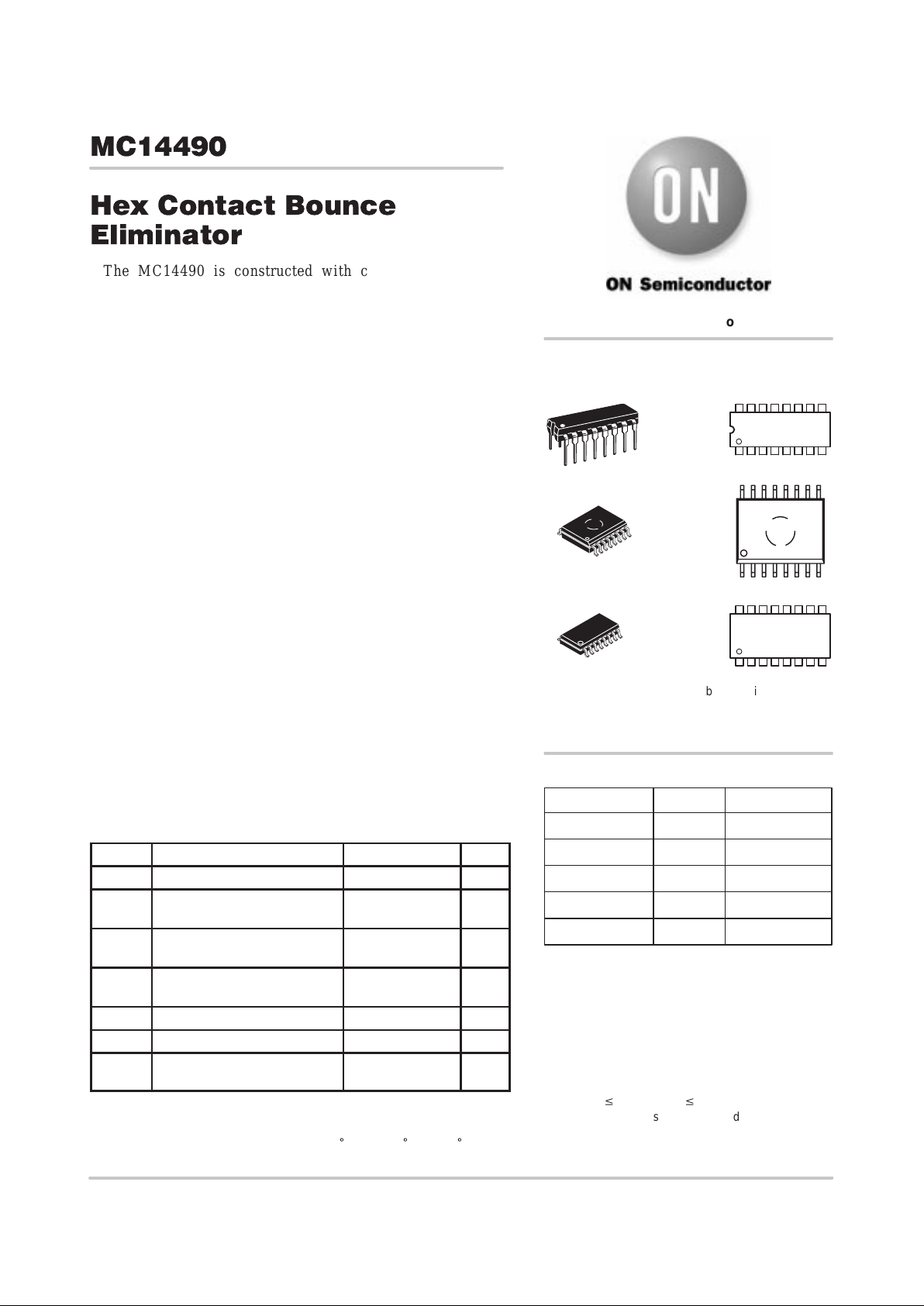
MC14490
Hex Contact Bounce
Eliminator
The MC14490 is constructed with complementary MOS
enhancement mode devices, and is used for the elimination of
extraneous level changes that result when interfacing with mechanical
contacts. The digital contact bounce eliminator circuit takes an input
signal from a bouncing contact and generates a clean digital signal
four clock periods after the input has stabilized. The bounce eliminator
circuit will remove bounce on both the “make” and the “break” of a
contact closure. The clock for operation of the MC14490 is derived
from an internal R–C oscillator which requires only an external
capacitor to adjust for the desired operating frequency (bounce delay).
The clock may also be driven from an external clock source or the
oscillator of another MC14490 (see Figure 5).
NOTE: Immediately after power–up, the outputs of the MC14490
are in indeterminate states.
• Diode Protection on All Inputs
• Six Debouncers Per Package
• Internal Pullups on All Data Inputs
• Can Be Used as a Digital Integrator, System Synchronizer, or Delay
Line
• Internal Oscillator (R–C), or External Clock Source
• TTL Compatible Data Inputs/Outputs
• Single Line Input, Debounces Both “Make” and “Break” Contacts
• Does Not Require “Form C” (Single Pole Double Throw) Input
Signal
• Cascadable for Longer Time Delays
• Schmitt Trigger on Clock Input (Pin 7)
• Supply Voltage Range = 3.0 V to 18 V
• Chip Complexity: 546 FETs or 136.5 Equivalent Gates
MAXIMUM RATINGS (Voltages Referenced to V
SS
) (Note 2.)
Symbol Parameter Value Unit
V
DD
DC Supply Voltage Range –0.5 to +18.0 V
Vin, V
out
Input or Output Voltage Range
(DC or Transient)
–0.5 to VDD + 0.5 V
I
in
Input Current
(DC or Transient) per Pin
±10 mA
P
D
Power Dissipation,
per Package (Note 3.)
500 mW
T
A
Ambient Temperature Range –55 to +125 °C
T
stg
Storage Temperature Range –65 to +150 °C
T
L
Lead Temperature
(8–Second Soldering)
260 °C
2. Maximum Ratings are those values beyond which damage to the device
may occur.
3. Temperature Derating:
Plastic “P and D/DW” Packages: – 7.0 mW/_C From 65_C T o 125_C
http://onsemi.com
A = Assembly Location
WL or L = Wafer Lot
YY or Y = Year
WW or W = Work Week
Device Package Shipping
ORDERING INFORMATION
MC14490DW SOIC–16 47/Rail
MC14490DWR2 SOIC–16 1000/Tape & Reel
MC14490F SOEIAJ–16 See Note 1.
1. For ordering information on the EIAJ version of
the SOIC packages, please contact your local
ON Semiconductor representative.
MARKING
DIAGRAMS
1
16
PDIP–16
P SUFFIX
CASE 648
MC14490P
AWLYYWW
MC14490FEL SOEIAJ–16 See Note 1.
MC14490P PDIP–16 25/Rail
SOIC–16
DW SUFFIX
CASE 751G
1
16
14490
AWLYYWW
This device contains protection circuitry to guard
against damage due to high static voltages or electric
fields. However, precautions must be taken to avoid applications of any voltage higher than maximum rated
voltages to this high–impedance circuit. For proper
operation, V
in
and V
out
should be constrained to the
range V
SS
v (Vin or V
out
) v VDD.
Unused inputs must always be tied to an appropriate
logic voltage level (e.g., either V
SS
or VDD). Unused out-
puts must be left open.
SOEIAJ–16
F SUFFIX
CASE 966
1
16
MC14490
AWLYWW
Page 2
MC14490
http://onsemi.com
2
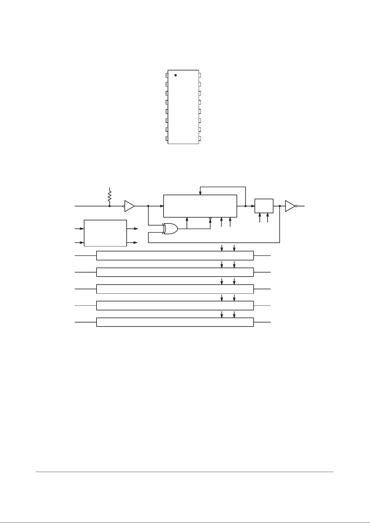
PIN ASSIGNMENT
13
14
15
16
9
10
11
125
4
3
2
1
8
7
6
D
in
C
out
B
in
V
DD
OSC
out
F
in
E
out
D
out
C
in
B
out
A
in
V
SS
OSC
in
F
out
E
in
A
out
BLOCK DIAGRAM
Ain1
OSC
in
7
OSC
out
9
B
in
14
C
in
3
D
in
12
Ein5
F
in
10
+V
DD
φ1
φ2
OSCILLATOR
AND
TWO–PHASE
CLOCK GENERATOR
DATA
SHIFT LOAD
4–BIT STATIC SHIFT REGISTER
1/2–BIT
DELAY
φ1 φ2
φ1 φ2
15 A
out
VDD = PIN 16
V
SS
= PIN 8
φ1 φ2
φ1 φ2
φ1 φ2
φ1 φ2
φ1 φ2
2B
out
13 C
out
4D
out
11 E
out
6F
out
IDENTICAL TO ABOVE STAGE
IDENTICAL TO ABOVE STAGE
IDENTICAL TO ABOVE STAGE
IDENTICAL TO ABOVE STAGE
IDENTICAL TO ABOVE STAGE
Page 3
MC14490
http://onsemi.com
3
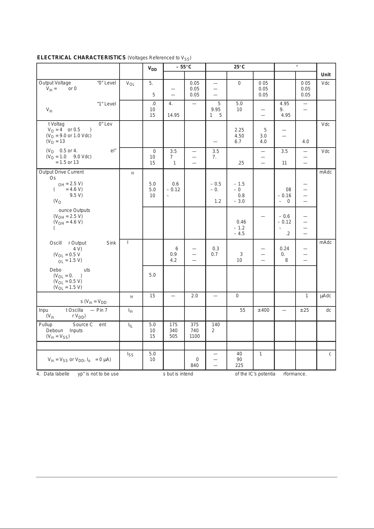
ELECTRICAL CHARACTERISTICS (Voltages Referenced to V
SS
)
V
DD
– 55_C
25_C
125_C
Characteristic
Symbol
DD
Vdc
Min
Max
Min
Typ
(4.)
Max
Min
Max
Unit
ОООООООО
Î
Output Voltage “0” Level
Vin = VDD or 0
ÎÎ
Î
V
OL
Î
Î
5.0
10
15
Î
Î
—
—
—
Î
Î
0.05
0.05
0.05
ÎÎ
Î
—
—
—
Î
Î
0
0
0
ÎÎ
Î
0.05
0.05
0.05
Î
Î
—
—
—
Î
Î
0.05
0.05
0.05
Î
Î
Vdc
ОООООООО
Î
“1” Level
Vin = 0 or V
DD
ÎÎ
Î
V
OH
Î
Î
5.0
10
15
Î
Î
4.95
9.95
14.95
Î
Î
—
—
—
ÎÎ
Î
4.95
9.95
14.95
Î
Î
5.0
10
15
ÎÎ
Î
—
—
—
Î
Î
4.95
9.95
14.95
Î
Î
—
—
—
Î
Î
Vdc
ОООООООО
Î
ОООООООО
Î
Input Voltage “0” Level
(VO = 4.5 or 0.5 Vdc)
(V
O
= 9.0 or 1.0 Vdc)
(VO = 13.5 or 1.5 Vdc)
ÎÎ
Î
ÎÎ
Î
V
IL
Î
Î
Î
Î
5.0
10
15
Î
Î
Î
Î
—
—
—
Î
Î
Î
Î
1.5
3.0
4.0
ÎÎ
Î
ÎÎ
Î
—
—
—
Î
Î
Î
Î
2.25
4.50
6.75
ÎÎ
Î
ÎÎ
Î
1.5
3.0
4.0
Î
Î
Î
Î
—
—
—
Î
Î
Î
Î
1.5
3.0
4.0
Î
Î
Î
Î
Vdc
ОООООООО
Î
(VO = 0.5 or 4.5 Vdc) “1 Level”
(VO = 1.0 or 9.0 Vdc)
(VO = 1.5 or 13.5 Vdc)
ÎÎ
Î
V
IH
Î
Î
5.0
10
15
Î
Î
3.5
7.0
11
Î
Î
—
—
—
ÎÎ
Î
3.5
7.0
11
Î
Î
2.75
5.50
8.25
ÎÎ
Î
—
—
—
Î
Î
3.5
7.0
11
Î
Î
—
—
—
Î
Î
Vdc
ОООООООО
Î
ОООООООО
Î
ОООООООО
Î
Output Drive Current
Oscillator Output Source
(VOH = 2.5 V)
(V
OH
= 4.6 V)
(VOH = 9.5 V)
(VOH = 13.5 V)
ÎÎ
Î
ÎÎ
Î
ÎÎ
Î
I
OH
Î
Î
Î
Î
Î
Î
5.0
5.0
10
15
Î
Î
Î
Î
Î
Î
– 0.6
– 0.12
– 0.23
– 1.4
Î
Î
Î
Î
Î
Î
—
—
—
—
ÎÎ
Î
ÎÎ
Î
ÎÎ
Î
– 0.5
– 0.1
– 0.2
– 1.2
Î
Î
Î
Î
Î
Î
– 1.5
– 0.3
– 0.8
– 3.0
ÎÎ
Î
ÎÎ
Î
ÎÎ
Î
—
—
—
—
Î
Î
Î
Î
Î
Î
– 0.4
– 0.08
– 0.16
– 1.0
Î
Î
Î
Î
Î
Î
—
—
—
—
Î
Î
Î
Î
Î
Î
mAdc
ОООООООО
Î
ОООООООО
Î
ОООООООО
Î
Debounce Outputs
(V
OH
= 2.5 V)
(V
OH
= 4.6 V)
(VOH = 9.5 V)
(VOH = 13.5 V)
ÎÎ
Î
ÎÎ
Î
ÎÎ
Î
Î
Î
Î
Î
Î
Î
5.0
5.0
10
15
Î
Î
Î
Î
Î
Î
– 0.9
– 0.19
– 0.6
1.8
Î
Î
Î
Î
Î
Î
—
—
—
—
ÎÎ
Î
ÎÎ
Î
ÎÎ
Î
– 0.75
– 0.16
– 0.5
– 1.5
Î
Î
Î
Î
Î
Î
– 2.2
– 0.46
– 1.2
– 4.5
ÎÎ
Î
ÎÎ
Î
ÎÎ
Î
—
—
—
—
Î
Î
Î
Î
Î
Î
– 0.6
– 0.12
– 0.4
– 1.2
Î
Î
Î
Î
Î
Î
—
—
—
—
Î
Î
Î
Î
Î
Î
ОООООООО
Î
Oscillator Output Sink
(VOL = 0.4 V)
(VOL = 0.5 V)
(V
OL
= 1.5 V)
ÎÎ
Î
I
OL
Î
Î
5.0
10
15
Î
Î
0.36
0.9
4.2
Î
Î
—
—
—
ÎÎ
Î
0.3
0.75
3.5
Î
Î
0.9
2.3
10
ÎÎ
Î
—
—
—
Î
Î
0.24
0.6
2.8
Î
Î
—
—
—
Î
Î
mAdc
ОООООООО
Î
ОООООООО
Î
Debounce Outputs
(V
OL
= 0.4 V)
(VOL = 0.5 V)
(VOL = 1.5 V)
ÎÎ
Î
ÎÎ
Î
Î
Î
Î
Î
5.0
10
15
Î
Î
Î
Î
2.6
4.0
12
Î
Î
Î
Î
—
—
—
ÎÎ
Î
ÎÎ
Î
2.2
3.3
10
Î
Î
Î
Î
4.0
9.0
35
ÎÎ
Î
ÎÎ
Î
—
—
—
Î
Î
Î
Î
1.8
2.7
8.1
Î
Î
Î
Î
—
—
—
Î
Î
Î
Î
ОООООООО
Î
Input Current
Debounce Inputs (V
in
= VDD)
ÎÎ
Î
I
IH
Î
Î
15
Î
Î
—
Î
Î
2.0
ÎÎ
Î
—
Î
Î
0.2
ÎÎ
Î
2.0
Î
Î
—
Î
Î
11
Î
Î
µAdc
Input Current Oscillator — Pin 7
(Vin = VSS or VDD)
I
in
15
—
± 620
—
± 255
± 400
—
± 250
µAdc
ОООООООО
Î
Pullup Resistor Source Current
Debounce Inputs
(Vin = VSS)
ÎÎ
Î
I
IL
Î
Î
5.0
10
15
Î
Î
175
340
505
Î
Î
375
740
1100
ÎÎ
Î
140
280
415
Î
Î
190
380
570
ÎÎ
Î
255
500
750
Î
Î
70
145
215
Î
Î
225
440
660
Î
Î
µAdc
Input Capacitance
C
in
—
—
—
—
5.0
7.5
—
—
pF
ОООООООО
Î
ОООООООО
Î
Quiescent Current
(Vin = VSS or VDD, I
out
= 0 µA)
ÎÎ
Î
ÎÎ
Î
I
SS
Î
Î
Î
Î
5.0
10
15
Î
Î
Î
Î
—
—
—
Î
Î
Î
Î
150
280
840
ÎÎ
Î
ÎÎ
Î
—
—
—
Î
Î
Î
Î
40
90
225
ÎÎ
Î
ÎÎ
Î
100
225
650
Î
Î
Î
Î
—
—
—
Î
Î
Î
Î
90
180
550
Î
Î
Î
Î
µAdc
4. Data labelled “Typ” is not to be used for design purposes but is intended as an indication of the IC’s potential performance.
Page 4
MC14490
http://onsemi.com
4
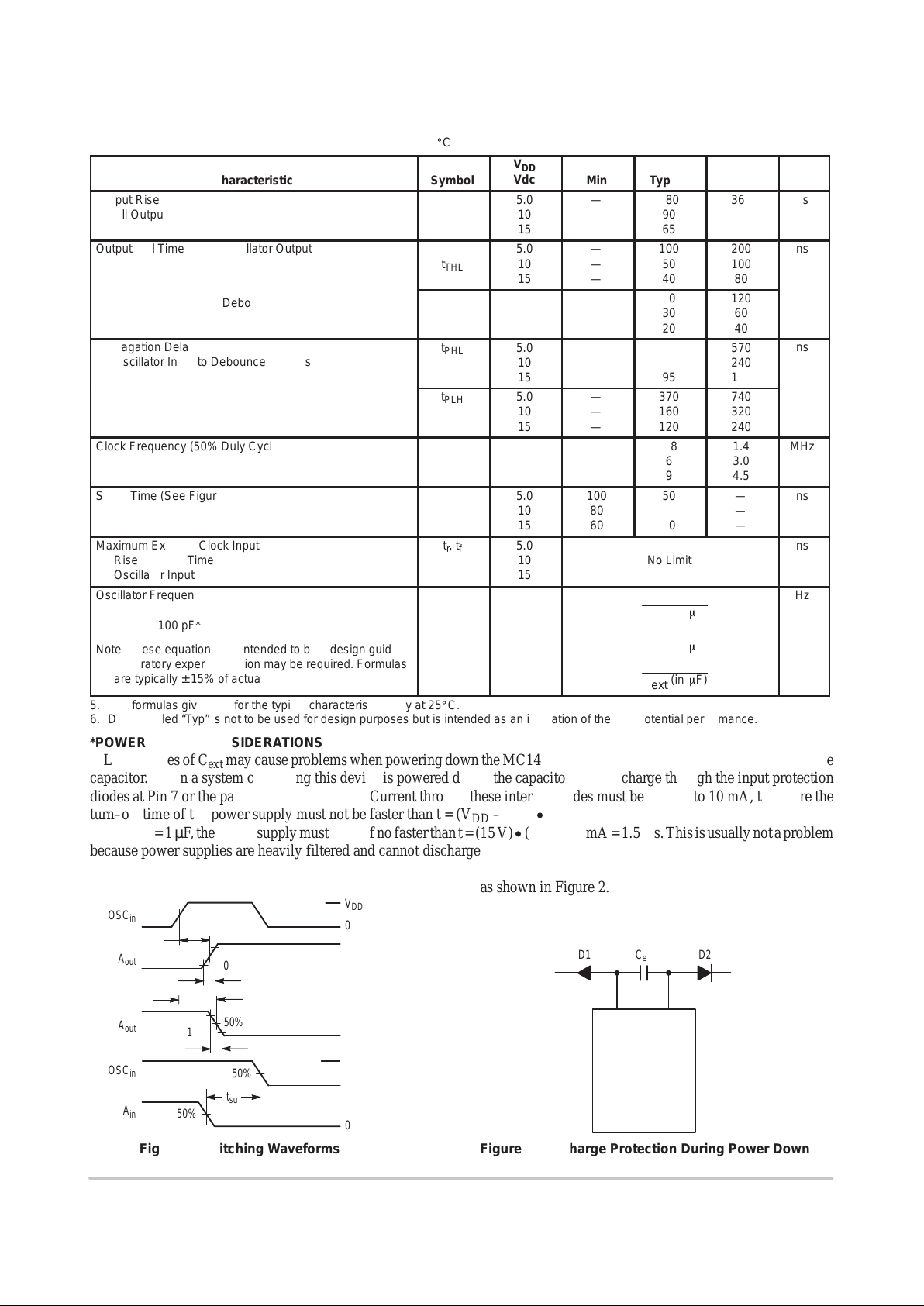
SWITCHING CHARACTERISTICS
(5.)
(C
L
= 50 pF, T
A
= 25_C)
Characteristic
ÎÎÎÎ
Symbol
V
DD
Vdc
Min
Typ
(6.)
Max
Unit
ОООООООООООООО
Î
Output Rise Time
All Outputs
ÎÎÎÎ
ÎÎÎ
Î
t
TLH
ÎÎ
Î
5.0
10
15
ÎÎ
Î
—
—
—
ÎÎ
Î
180
90
65
ÎÎ
Î
360
180
130
Î
Î
ns
ОООООООООООООО
Î
ОООООООООООООО
Î
Output Fall Time Oscillator Output
ÎÎÎÎ
ÎÎÎ
Î
ÎÎÎ
Î
t
THL
ÎÎ
Î
ÎÎ
Î
5.0
10
15
ÎÎ
Î
ÎÎ
Î
—
—
—
ÎÎ
Î
ÎÎ
Î
100
50
40
ÎÎ
Î
ÎÎ
Î
200
100
80
Î
Î
Î
Î
ns
ОООООООООООООО
Î
Debounce Outputs
ÎÎÎÎ
ÎÎÎ
Î
t
THL
ÎÎ
Î
5.0
10
15
ÎÎ
Î
—
—
—
ÎÎ
Î
60
30
20
ÎÎ
Î
120
60
40
Î
Î
ОООООООООООООО
Î
Propagation Delay Time
Oscillator Input to Debounce Outputs
ÎÎÎÎ
ÎÎÎ
Î
t
PHL
ÎÎ
Î
5.0
10
15
ÎÎ
Î
—
—
—
ÎÎ
Î
285
120
95
ÎÎ
Î
570
240
190
Î
Î
ns
ОООООООООООООО
Î
ÎÎÎÎ
ÎÎÎ
Î
t
PLH
ÎÎ
Î
5.0
10
15
ÎÎ
Î
—
—
—
ÎÎ
Î
370
160
120
ÎÎ
Î
740
320
240
Î
Î
ОООООООООООООО
Î
Clock Frequency (50% Duly Cycle)
(External Clock)
ÎÎÎÎ
ÎÎÎ
Î
f
cl
ÎÎ
Î
5.0
10
15
ÎÎ
Î
—
—
—
ÎÎ
Î
2.8
6
9
ÎÎ
Î
1.4
3.0
4.5
Î
Î
MHz
ОООООООООООООО
Î
Setup Time (See Figure 1)
ÎÎÎÎ
ÎÎÎ
Î
t
su
ÎÎ
Î
5.0
10
15
ÎÎ
Î
100
80
60
ÎÎ
Î
50
40
30
ÎÎ
Î
—
—
—
Î
Î
ns
ОООООООООООООО
Î
Maximum External Clock Input
Rise and Fall Time
Oscillator Input
ÎÎÎÎ
ÎÎÎ
Î
tr, t
f
ÎÎ
Î
5.0
10
15
ОООООООО
Î
No Limit
Î
Î
ns
ОООООООООООООО
Î
ОООООООООООООО
Î
ОООООООООООООО
Î
ОООООООООООООО
Î
Oscillator Frequency
OSC
out
C
ext
≥ 100 pF*
Note: These equations are intended to be a design guide.
Laboratory experimentation may be required. Formulas
are typically ± 15% of actual frequencies.
ÎÎÎÎ
ÎÎÎ
Î
ÎÎÎ
Î
ÎÎÎ
Î
ÎÎÎ
Î
f
osc
, typ
ÎÎ
Î
ÎÎ
Î
ÎÎ
Î
ÎÎ
Î
5.0
10
15
ОООООООО
Î
ОООООООО
Î
ОООООООО
Î
ОООООООО
Î
1.5
C
ext
(inmF)
4.5
C
ext
(inmF)
6.5
C
ext
(inmF)
Î
Î
Î
Î
Î
Î
Î
Î
Hz
5. The formulas given are for the typical characteristics only at 25_C.
6. Data labelled “Typ” is not to be used for design purposes but is intended as an indication of the IC’s potential performance.
*POWER–DOWN CONSIDERATIONS
Large values of C
ext
may cause problems when powering down the MC14490 because of the amount of energy stored in the
capacitor. When a system containing this device is powered down, the capacitor may discharge through the input protection
diodes at Pin 7 or the parasitic diodes at Pin 9. Current through these internal diodes must be limited to 10 mA, therefore the
turn–off time of the power supply must not be faster than t = (VDD – VSS) C
ext
/(10 mA). For example, If VDD – VSS = 15
V and C
ext
= 1 µF , the power supply must turn off no faster than t = (15 V) (1 µF)/10 mA = 1.5 ms. This is usually not a problem
because power supplies are heavily filtered and cannot discharge at this rate.
When a more rapid decrease of the power supply to zero volts occurs, the MC14490 may sustain damage. To avoid this
possibility, use external clamping diodes, D1 and D2, connected as shown in Figure 2.
Figure 1. Switching Waveforms Figure 2. Discharge Protection During Power Down
OSC
in
A
out
A
out
OSC
in
A
in
V
DD
0 V
V
DD
0 V
V
DD
0 V
50%
90%
50%
10%
t
r
t
f
t
PHL
90%
10%
50%
50%
t
su
50%
D1 D2C
ext
9
7
OSC
in
OSC
out
MC14490
t
PLH
V
DD
V
DD
Page 5

MC14490
http://onsemi.com
5
THEORY OF OPERATION
The MC14490 Hex Contact Bounce Eliminator is
basically a digital integrator. The circuit can integrate both
up and down. This enables the circuit to eliminate bounce on
both the leading and trailing edges of the signal, shown in the
timing diagram of Figure 3.
Each of the six Bounce Eliminators is composed of a
4–1/2–bit register (the integrator) and logic to compare the
input with the contents of the shift register, as shown in
Figure 4. The shift register requires a series of timing pulses
in order to shift the input signal into each shift register
location. These timing pulses (the clock signal) are
represented in the upper waveform of Figure 3. Each of the
six Bounce Eliminator circuits has an internal resistor as
shown in Figure 4. A pullup resistor was incorporated rather
than a pulldown resistor in order to implement switched
ground input signals, such as those coming from relay
contacts and push buttons. By switching ground, rather than
a power supply lead, system faults (such as shorts to ground
on the signal input leads) will not cause excessive currents
in the wiring and contacts. Signal lead shorts to ground are
much more probable than shorts to a power supply lead.
When the relay contact is closed, (see Figure 4) the low
level is inverted, and the shift register is loaded with a high
on each positive edge of the clock signal. To understand the
operation, we assume all bits of the shift register are loaded
with lows and the output is at a high level.
At clock edge 1 (Figure 3) the input has gone low and a
high has been loaded into the first bit or storage location of
the shift register. Just after the positive edge of clock 1, the
input signal has bounced back to a high. This causes the shift
register to be reset to lows in all four bits — thus starting the
timing sequence over again.
During clock edges 3 to 6 the input signal has stayed low.
Thus, a high has been shifted into all four shift register bits
and, as shown, the output goes low during the positive edge
of clock pulse 6.
It should be noted that there is a 3–1/2 to 4–1/2 clock
period delay between the clean input signal and output
signal. In this example there is a delay of 3.8 clock periods
from the beginning of the clean input signal.
After some time period of N clock periods, the contact is
opened and at N+1 a low is loaded into the first bit. Just after
N+1, when the input bounces low, all bits are set to a high.
At N+2 nothing happens because the input and output are
low and all bits of the shift register are high. At time N+3
and thereafter the input signal is a high, clean signal. At the
positive edge of N+6 the output goes high as a result of four
lows being shifted into the shift register.
Assuming the input signal is long enough to be clocked
through the Bounce Eliminator, the output signal will be no
longer or shorter than the clean input signal plus or minus
one clock period.
The amount of time distortion between the input and
output signals is a function of the difference in bounce
characteristics on the edges of the input signal and the clock
frequency. Since most relay contacts have more bounce
when making as compared to breaking, the overall delay,
counting bounce period, will be greater on the leading edge
of the input signal than on the trailing edge. Thus, the output
signal will be shorter than the input signal — if the leading
edge bounce is included in the overall timing calculation.
The only requirement on the clock frequency in order to
obtain a bounce free output signal is that four clock periods
do not occur while the input signal is in a false state.
Referring to Figure 3, a false state is seen to occur three times
at the beginning of the input signal. The input signal goes
low three times before it finally settles down to a valid low
state. The first three low pulses are referred to as false states.
If the user has an available clock signal of the proper
frequency, it may be used by connecting it to the oscillator
input (pin 7). However, if an external clock is not available
the user can place a small capacitor across the oscillator
input and output pins in order to start up an internal clock
source (as shown in Figure 4). The clock signal at the
oscillator output pin may then be used to clock other
MC14490 Bounce Eliminator packages. With the use of the
MC14490, a large number of signals can be cleaned up, with
the requirement of only one small capacitor external to the
Hex Bounce Eliminator packages.
Figure 3. Timing Diagram
OSCin OR OSC
out
INPUT
OUTPUT
CONTACT
OPEN
CONTACT
BOUNCING
CONTACT CLOSED
(VALID TRUE SIGNAL)
CONTACT
BOUNCING
CONTACT OPEN
N + 7N + 5N + 3N + 1654321
Page 6

MC14490
http://onsemi.com
6
Figure 4. Typical “Form A” Contact Debounce Circuit
(Only One Debouncer Shown)
1/2 BIT
DELAY
OSCILLATOR
AND
TWO–PHASE
CLOCK GENERATOR
C
ext
OSC
out
OSC
in
“FORM A”
CONTACT
A
in
1
9
7
φ1
φ2
DATA
SHIFT LOAD
4–BIT STATIC SHIFT REGISTER
φ1 φ2
φ1 φ2
15
A
out
+V
DD
PULLUP RESISTOR
(INTERNAL)
OPERA TING CHARACTERISTICS
The single most important characteristic of the MC14490
is that it works with a single signal lead as an input, making
it directly compatible with mechanical contacts (Form A
and B).
The circuit has a built–in pullup resistor on each input.
The worst case value of the pullup resistor (determined from
the Electrical Characteristics table) is used to calculate the
contact wetting current. If more contact current is required,
an external resistor may be connected between V
DD
and the
input.
Because of the built–in pullup resistors, the inputs cannot
be driven with a single standard CMOS gate when V
DD
is
below 5 V. At this voltage, the input should be driven with
paralleled standard gates or by the MC14049 or MC14050
buffers.
The clock input circuit (pin 7) has Schmitt trigger shaping
such that proper clocking will occur even with very slow
clock edges, eliminating any need for clock preshaping. In
addition, other MC14490 oscillator inputs can be driven
from a single oscillator output buffered by an MC14050 (see
Figure 5). Up to six MC14490s may be driven by a single
buffer.
The MC14490 is TTL compatible on both the inputs and
the outputs. When V
DD
is at 4.5 V, the buffered outputs can
sink 1.6 mA at 0.4 V. The inputs can be driven with TTL as
a result of the internal input pullup resistors.
Figure 5. Typical Single Oscillator Debounce System
FROM CONTACTS MC14490
TO SYSTEM
LOGIC
OSC
in
OSC
out
C
ext
1/6 MC14050
97
OSC
in
7 9 OSC
out
NO CONNECTION
FROM
CONTACTS
TO SYSTEM
LOGIC
MC14490
NO CONNECTION
9 OSC
out
OSCin7
FROM CONTACTS MC14490
TO SYSTEM
LOGIC
Page 7

MC14490
http://onsemi.com
7
TYPICAL APPLICATIONS
ASYMMETRICAL TIMING
In applications where different leading and trailing edge
delays are required (such as a fast attack/slow release timer.)
Clocks of different frequencies can be gated into the
MC14490 as shown in Figure 6. In order to produce a slow
attack/fast release circuit leads A and B should be
interchanged. The clock out lead can then be used to feed
clock signals to the other MC14490 packages where the
asymmetrical input/output timing is required.
Figure 6. Fast Attack/Slow Release Circuit
IN OUT
OSC
out
MC14011B
OSC
in
AB
f
C/N
EXTERNAL
CLOCK
÷ N
f
C
MC14490
LATCHED OUTPUT
The contents of the Bounce Eliminator can be latched by
using several extra gates as shown in Figure 7. If the latch
lead is high the clock will be stopped when the output goes
low. This will hold the output low even though the input has
returned to the high state. Any time the clock is stopped the
outputs will be representative of the input signal four clock
periods earlier.
Figure 7. Latched Output Circuit
IN OUT
OSC
out
MC14011B
OSC
in
MC14490
CLOCK
LATCH = 1
UNLATCH = 0
MULTIPLE TIMING SIGNALS
As shown in Figure 8, the Bounce Eliminator circuits can
be connected in series. In this configuration each output is
delayed by four clock periods relative to its respective input.
This configuration may be used to generate multiple timing
signals such as a delay line, for programming other timing
operations.
One application of the above is shown in Figure 9, where
it is required to have a single pulse output for a single
operation (make) of the push button or relay contact. This
only requires the series connection of two Bounce
Eliminator circuits, one inverter, and one NOR gate in order
to generate the signal A
B as shown in Figures 9 and 10. The
signal AB is four clock periods in length. If the inverter is
switched to the A output, the pulse AB will be generated
upon release or break of the contact. With the use of a few
additional parts many different pulses and waveshapes may
be generated.
Figure 8. Multiple Timing Circuit Connections
10
5
12
3
14
1
79
6
11
4
13
2
15
A
out
B
out
C
out
D
out
E
out
F
out
OSC
in
CLOCK
B.E. 6
B.E. 5
B.E. 4
B.E. 3
B.E. 2
B.E. 1
OSC
out
A
in
B
in
C
in
D
in
E
in
F
in
Page 8

MC14490
http://onsemi.com
8
Figure 9. Single Pulse Output Circuit
IN
IN
A
OUT
OUT
B
A
B
AB
A ≡ ACTIVE LOW
B ≡ ACTIVE LOW
BE 2
BE 1
Figure 10. Multiple Output Signal Timing Diagram
OSCin OR
OSC
out
INPUT
A
B
C
D
E
F
A
B
AB
Page 9

MC14490
http://onsemi.com
9
P ACKAGE DIMENSIONS
PDIP–16
P SUFFIX
PLASTIC DIP PACKAGE
CASE 648–08
ISSUE R
NOTES:
1. DIMENSIONING AND TOLERANCING PER ANSI
Y14.5M, 1982.
2. CONTROLLING DIMENSION: INCH.
3. DIMENSION L TO CENTER OF LEADS WHEN
FORMED PARALLEL.
4. DIMENSION B DOES NOT INCLUDE MOLD FLASH.
5. ROUNDED CORNERS OPTIONAL.
–A–
B
F
C
S
H
G
D
J
L
M
16 PL
SEATING
18
916
K
PLANE
–T–
M
A
M
0.25 (0.010) T
DIM MIN MAX MIN MAX
MILLIMETERSINCHES
A 0.740 0.770 18.80 19.55
B 0.250 0.270 6.35 6.85
C 0.145 0.175 3.69 4.44
D 0.015 0.021 0.39 0.53
F 0.040 0.70 1.02 1.77
G 0.100 BSC 2.54 BSC
H 0.050 BSC 1.27 BSC
J 0.008 0.015 0.21 0.38
K 0.110 0.130 2.80 3.30
L 0.295 0.305 7.50 7.74
M 0 10 0 10
S 0.020 0.040 0.51 1.01
____
Page 10

MC14490
http://onsemi.com
10
P ACKAGE DIMENSIONS
H
E
A
1
DIM MIN MAX MIN MAX
INCHES
––– 2.05 ––– 0.081
MILLIMETERS
0.05 0.20 0.002 0.008
0.35 0.50 0.014 0.020
0.18 0.27 0.007 0.011
9.90 10.50 0.390 0.413
5.10 5.45 0.201 0.215
1.27 BSC 0.050 BSC
7.40 8.20 0.291 0.323
0.50 0.85 0.020 0.033
1.10 1.50 0.043 0.059
0
0.70 0.90 0.028 0.035
––– 0.78 ––– 0.031
A
1
H
E
Q
1
L
E
_
10
_
0
_
10
_
L
E
Q
1
_
NOTES:
1. DIMENSIONING AND TOLERANCING PER ANSI
Y14.5M, 1982.
2. CONTROLLING DIMENSION: MILLIMETER.
3. DIMENSIONS D AND E DO NOT INCLUDE
MOLD FLASH OR PROTRUSIONS AND ARE
MEASURED AT THE PARTING LINE. MOLD FLASH
OR PROTRUSIONS SHALL NOT EXCEED 0.15
(0.006) PER SIDE.
4. TERMINAL NUMBERS ARE SHOWN FOR
REFERENCE ONLY.
5. THE LEAD WIDTH DIMENSION (b) DOES NOT
INCLUDE DAMBAR PROTRUSION. ALLOWABLE
DAMBAR PROTRUSION SHALL BE 0.08 (0.003)
TOTAL IN EXCESS OF THE LEAD WIDTH
DIMENSION AT MAXIMUM MATERIAL CONDITION.
DAMBAR CANNOT BE LOCATED ON THE LOWER
RADIUS OR THE FOOT. MINIMUM SPACE
BETWEEN PROTRUSIONS AND ADJACENT LEAD
TO BE 0.46 ( 0.018).
M
L
DETAIL P
VIEW P
c
A
b
e
M
0.13 (0.005)
0.10 (0.004)
1
16 9
8
D
Z
E
A
b
c
D
E
e
L
M
Z
SOEIAJ–16
F SUFFIX
PLASTIC EIAJ SOIC PACKAGE
CASE 966–01
ISSUE O
Page 11

MC14490
http://onsemi.com
11
P ACKAGE DIMENSIONS
SOIC–16
DW SUFFIX
PLASTIC SOIC PACKAGE
CASE 751G–03
ISSUE B
D
14X
B16X
SEATING
PLANE
S
A
M
0.25 B
S
T
16 9
81
h X 45
_
M
B
M
0.25
H8X
E
B
A
e
T
A1
A
L
C
q
NOTES:
1. DIMENSIONS ARE IN MILLIMETERS.
2. INTERPRET DIMENSIONS AND TOLERANCES
PER ASME Y14.5M, 1994.
3. DIMENSIONS D AND E DO NOT INLCUDE MOLD
PROTRUSION.
4. MAXIMUM MOLD PROTRUSION 0.15 PER SIDE.
5. DIMENSION B DOES NOT INCLUDE DAMBAR
PROTRUSION. ALLOWABLE DAMBAR
PROTRUSION SHALL BE 0.13 TOTAL IN EXCESS
OF THE B DIMENSION AT MAXIMUM MATERIAL
CONDITION.
DIM MIN MAX
MILLIMETERS
A 2.35 2.65
A1 0.10 0.25
B 0.35 0.49
C 0.23 0.32
D 10.15 10.45
E 7.40 7.60
e 1.27 BSC
H 10.05 10.55
h 0.25 0.75
L 0.50 0.90
q
0 7
__
Page 12

MC14490
http://onsemi.com
12
ON Semiconductor and are trademarks of Semiconductor Components Industries, LLC (SCILLC). SCILLC reserves the right to make changes
without further notice to any products herein. SCILLC makes no warranty , representation or guarantee regarding the suitability of its products for any particular
purpose, nor does SCILLC assume any liability arising out of the application or use of any product or circuit, and specifically disclaims any and all liability ,
including without limitation special, consequential or incidental damages. “Typical” parameters which may be provided in SCILLC data sheets and/or
specifications can and do vary in different applications and actual performance may vary over time. All operating parameters, including “Typicals” must be
validated for each customer application by customer’s technical experts. SCILLC does not convey any license under its patent rights nor the rights of others.
SCILLC products are not designed, intended, or authorized for use as components in systems intended for surgical implant into the body, or other applications
intended to support or sustain life, or for any other application in which the failure of the SCILLC product could create a situation where personal injury or
death may occur. Should Buyer purchase or use SCILLC products for any such unintended or unauthorized application, Buyer shall indemnify and hold
SCILLC and its officers, employees, subsidiaries, affiliates, and distributors harmless against all claims, costs, damages, and expenses, and reasonable
attorney fees arising out of, directly or indirectly , any claim of personal injury or death associated with such unintended or unauthorized use, even if such claim
alleges that SCILLC was negligent regarding the design or manufacture of the part. SCILLC is an Equal Opportunity/Affirmative Action Employer .
PUBLICATION ORDERING INFORMATION
CENTRAL/SOUTH AMERICA:
Spanish Phone: 303–308–7143 (Mon–Fri 8:00am to 5:00pm MST)
Email: ONlit–spanish@hibbertco.com
ASIA/PACIFIC : LDC for ON Semiconductor – Asia Support
Phone: 303–675–2121 (Tue–Fri 9:00am to 1:00pm, Hong Kong Time)
T oll Free from Hong Kong & Singapore:
001–800–4422–3781
Email: ONlit–asia@hibbertco.com
JAPAN: ON Semiconductor, Japan Customer Focus Center
4–32–1 Nishi–Gotanda, Shinagawa–ku, T okyo, Japan 141–0031
Phone: 81–3–5740–2745
Email: r14525@onsemi.com
ON Semiconductor Website: http://onsemi.com
For additional information, please contact your local
Sales Representative.
MC14490/D
NORTH AMERICA Literature Fulfillment:
Literature Distribution Center for ON Semiconductor
P.O. Box 5163, Denver, Colorado 80217 USA
Phone: 303–675–2175 or 800–344–3860 T oll Free USA/Canada
Fax: 303–675–2176 or 800–344–3867 Toll Free USA/Canada
Email: ONlit@hibbertco.com
Fax Response Line: 303–675–2167 or 800–344–3810 T oll Free USA/Canada
N. American Technical Support: 800–282–9855 Toll Free USA/Canada
EUROPE: LDC for ON Semiconductor – European Support
German Phone: (+1) 303–308–7140 (M–F 1:00pm to 5:00pm Munich Time)
Email: ONlit–german@hibbertco.com
French Phone: (+1) 303–308–7141 (M–F 1:00pm to 5:00pm Toulouse T ime)
Email: ONlit–french@hibbertco.com
English Phone: (+1) 303–308–7142 (M–F 12:00pm to 5:00pm UK Time)
Email: ONlit@hibbertco.com
EUROPEAN TOLL–FREE ACCESS*: 00–800–4422–3781
*Available from Germany, France, Italy , England, Ireland
 Loading...