

Page 1
MC14469MOTOROLA
1
CMOS
The MC14469 receives one or two 11–bit words in a serial data stream. One
of the incoming words contains the address and when the address matches, the
MC14469 then transmits information in two 11–bit word data streams. Each of
the transmitted words contains eight data bits, an even parity bit, and start and
stop bits.
The received word contains seven address bits with the address of the
MC14469 set on seven pins. Therefore, 27 or 128 units can be interconnected
in simplex or full–duplex data transmission. In addition to the address received,
seven command bits may be received for general–purpose data or control use.
The MC14469 finds application in transmitting data from remote analog–to–
digital converters, remote MPUs, or remote digital transducers to the master
computer or MPU.
• Supply Voltage Range: 4.5 V to 18 V
• Low Quiescent Current: 75 µA Maximum @ 5 V, 25°C
• Guaranteed Data Rates to 4800 Baud @ 5 V, to 9600 Baud @ 12 V
• Receive — Serial to Parallel
Transmit — Parallel to Parallel
• Transmit and Receive Simultaneously in Full Duplex
• Crystal or Resonator Operation for On–Chip Oscillator
• See Application Note AN806A
• Chip Complexity: 1200 FETs or 300 Equivalent Gates
PIN ASSIGNMENTS
P SUFFIX
5
4
3
2
1
8
7
6
37
38
39
40
34
35
36
33
C6
C5
C4
C0
V
DD
C1
C2
C3
A0
RESET
OSC2
OSC1
A3
A2
A1
A4
13
12
11
10
9
16
15
14
29
30
31
32
26
27
28
25
S4
S3
S2
VAP
CS
SEND
S0
S1
ID1
ID0
A6
A5
ID4
ID3
ID2
ID5
17
20
19
18
22
23
24
21
TRO
S7
S6
S5
RI
ID7
ID6
V
SS
FN SUFFIX
2827262524232221201918
4041424344123456
29
30
31
32
33
34
35
36
37
38
39
17
16
15
14
13
12
11
10
9
8
7
S3
S2
S1
S0
SEND
NC
VAP
CS
C6
C5
C4
ID4
ID3
ID2
ID1
ID0
NC
A6
A5
A4
A3
A2
A1A0RESET
OSC2
OSC1NCC0C1C2
C3
V
DD
ID5
ID6
ID7
RI
V
NC
TRO
S7S6S5
S4
SS
NC = NO CONNECTION
Order this document
by MC14469/D
SEMICONDUCTOR TECHNICAL DATA
P SUFFIX
PLASTIC DIP
CASE 711
FN SUFFIX
PLCC PACKAGE
CASE 777
ORDERING INFORMATION
MC14469P Plastic DIP
MC14469FN PLCC Package
40
1
44
1
Motorola, Inc. 1995
Page 2
MC14469 MOTOROLA
2
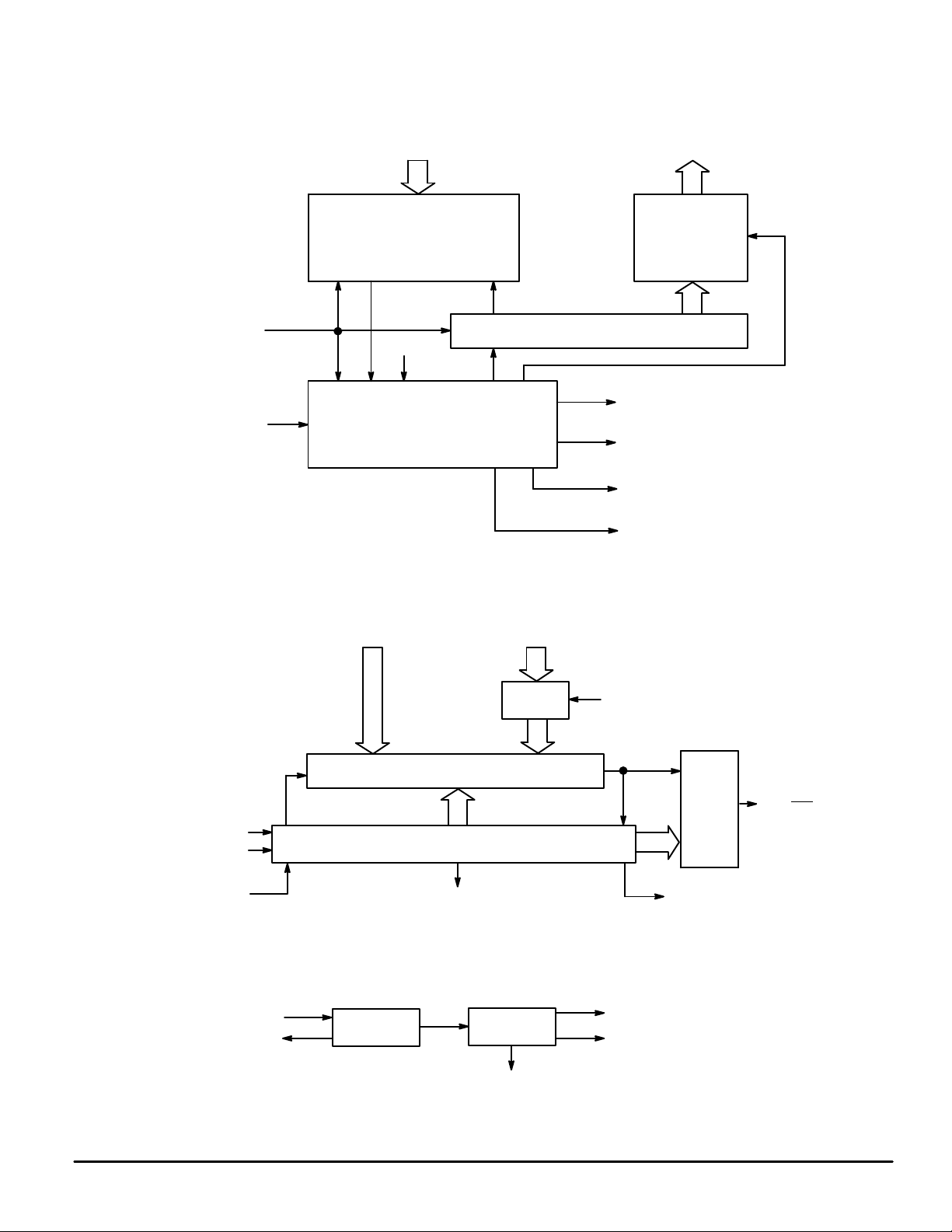
BLOCK DIAGRAM
CLOCKS
TRANSMIT
RECEIVE
STATUS
STROBE
(S0 – S7)
STATUS
2
LOAD
SELECT
STATIC SHIFT REGISTER
8
8
STATUS
LATCHES
8
CLOCK
DATA RATE CLOCK
SEND ENABLE
SEND
4
7
77
STATIC SHIFT REGISTER
TIMING AND CONTROL
AND PARITY CHECK
COMMAND
LATCHES
ADDRESS CONTROL
AND DATA COMPARATOR
RECEIVE
DATA
STROBE
RECEIVE
DATA
(RI)
CLOCK
COMPARE
CLOCK
RVAL
VALID ADDRESS
PULSE (VAP)
SEND ENABLE
LATCH (SEL)
RECEIVE DATA
STROBE ENABLE
COMMAND
STROBE (CS)
STROBE
(C0 – C6)
COMMAND DATA
(A0 – A6)
ADDRESS
RVAL
CLOCK
GENERATOR
CLOCK
OSCILLATOR
OUTPUT
LOGIC
CONTROL AND PARITY
GENERATOR
RECEIVE DATA STROBE ENABLE
RECEIVE DATA STROBE
OSC2
OSC1
STATUS STROBE
(ID0 – ID7)
INPUT DATA
DATA RATE CLOCK
TRANSMIT
DATA (TRO
)
Page 3
MC14469MOTOROLA
3
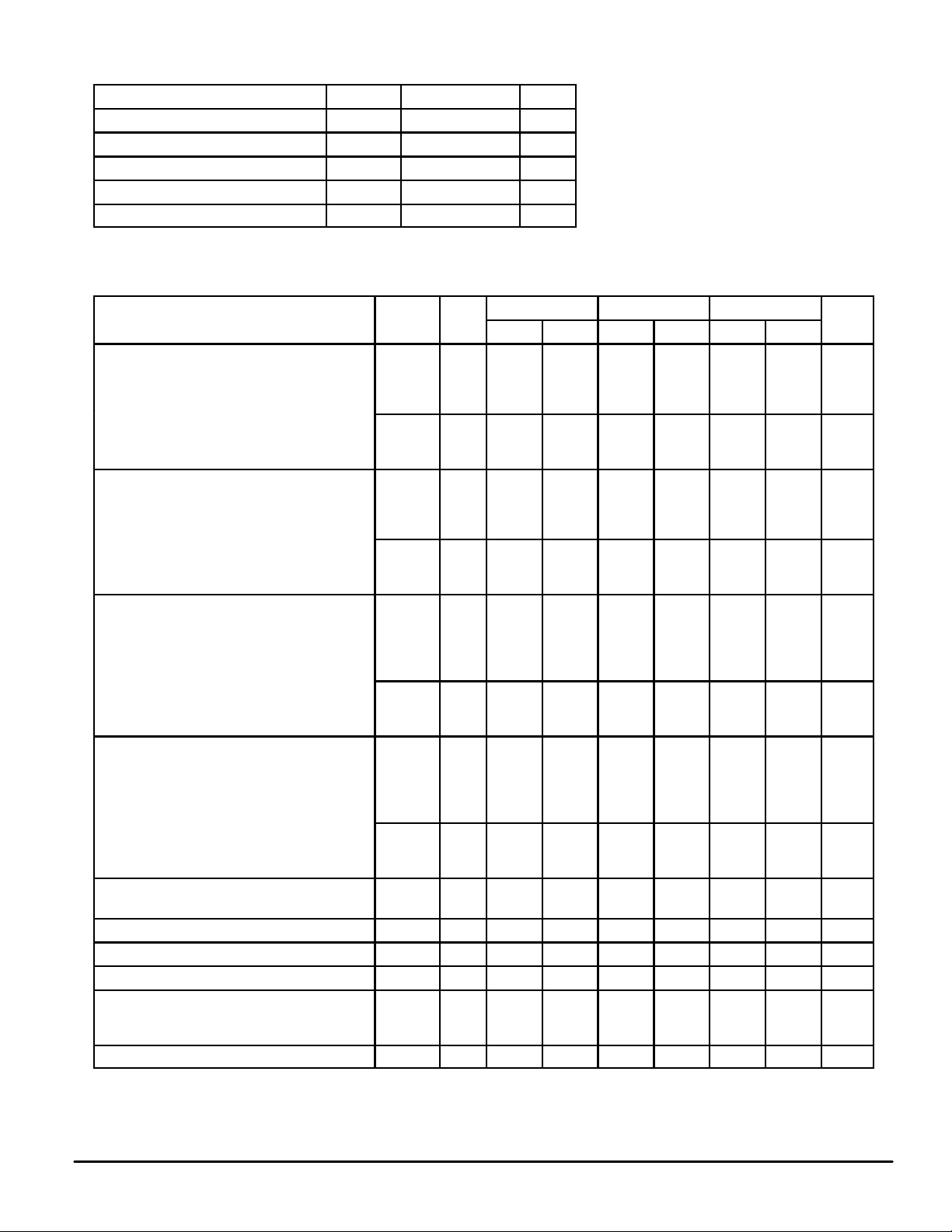
MAXIMUM RATINGS (Voltages referenced to V
SS
)
Rating
Symbol Value Unit
DC Supply Voltage V
DD
– 0.5 to + 18 V
Input Voltage, All Inputs V
in
– 0.5 to VDD + 0.5 V
DC Current Drain per Pin I 10 mA
Operating Temperature Range T
A
– 40 to + 85 °C
Storage Temperature Range T
stg
– 65 to + 150 °C
ELECTRICAL CHARACTERISTICS (Voltages referenced to V
SS
)
– 40°C 25°C 85°C
Characteristic Symbol
V
DD
Min Max Min Max Min Max Unit
Output Voltage
Vin= VDD or 0 “0” Level
V
OL
5.0
10
15
—
—
—
0.05
0.05
0.05
—
—
—
0.05
0.05
0.05
—
—
—
0.05
0.05
0.05
V
Vin= 0 or V
DD
“1” Level V
OH
5.0
10
15
4.95
9.95
14.95
—
—
—
4.95
9.95
14.95
—
—
—
4.95
9.95
14.95
—
—
—
V
Input Voltage (Except OSC1)
VO= 4.5 or 0.5 V “0” Level
VO= 9.0 or 1.0 V
VO= 13.5 or 1.5 V
V
IL
5.0
10
15
—
—
—
1.5
3.0
4.0
—
—
—
1.5
3.0
4.0
—
—
—
1.5
3.0
4.0
V
VO= 0.5 or 4.5 V “1” Level
VO= 1.0 or 9.0 V
VO= 1.5 or 13.5 V
V
IH
5.0
10
15
3.5
7.0
11
—
—
—
3.5
7.0
11
—
—
—
3.5
7.0
11
—
—
—
V
Output Drive Current (Except OSC2)
VOH= 2.5 V Source
VOH= 4.6 V
VOH= 9.5 V
VOH= 13.5 V
I
OH
5.0
5.0
10
15
– 1.0
– 0.2
– 0.5
– 1.4
—
—
—
—
– 0.8
– 0.16
– 0.4
– 1.2
—
—
—
—
– 0.6
– 0.12
– 0.3
– 1.0
—
—
—
—
mA
VOL= 0.4 V Sink
VOL= 0.5 V
VOL= 1.5 V
I
OL
5.0
10
15
0.52
1.3
3.6
—
—
—
0.44
1.1
3.0
—
—
—
0.36
0.9
2.4
—
—
—
mA
Output Drive Current (OSC2 Only)
VOH= 2.5 V Source
VOH= 4.6 V
VOH= 9.5 V
VOH= 13.5 V
I
OH
5.0
5.0
10
15
– 0.19
– 0.04
– 0.09
– 0.29
—
—
—
—
– 0.16
– 0.035
– 0.08
– 0.27
—
—
—
—
– 0.13
– 0.03
– 0.06
– 0.2
—
—
—
—
mA
VOL= 0.4 V Sink
VOL= 0.5 V
VOL= 1.5 V
I
OL
5.0
10
15
0.1
0.17
0.5
—
—
—
0.085
0.14
0.42
—
—
—
0.07
0.1
0.3
—
—
—
mA
OSC Frequency* f
OSC
4.5
12
0
0
400
800
0
0
365
730
0
0
310
620
kHz
Input Current I
in
15 — ± 0.3 — ± 0.3 — ± 1.0 µA
Pull–Up Current (A0 – A6, ID0 – ID7) I
UP
15 12 120 10 100 8.0 85 µA
Input Capacitance (Vin = 0) C
in
— — — — 7.5 — — pF
Quiescent Current (Per Package) I
DD
5.0
10
15
—
—
—
75
150
300
—
—
—
75
150
300
—
—
—
565
1125
2250
µA
Supply Voltage V
DD
— + 4.5 + 18 + 4.5 + 18 + 4.5 + 18 V
*310 kHz at 85°C guarantees 4800 baud; 620 kHz at 85°C guarantees 9600 baud.
This device contains circuitry to protect the
inputs against damage due to high static voltages or electric fields; however, it is advised that
normal precautions be taken to avoid application
of any voltage higher than maximum rated
voltages to this high–impedance circuit. For
proper operation it is recommended that Vin and
V
out
be constrained to the range VSS ≤ (Vin or
V
out
) ≤ VDD.
Unused inputs must always be tied to an
appropriate logic voltage level (e.g., either V
SS
or VDD).
Page 4
MC14469 MOTOROLA
4
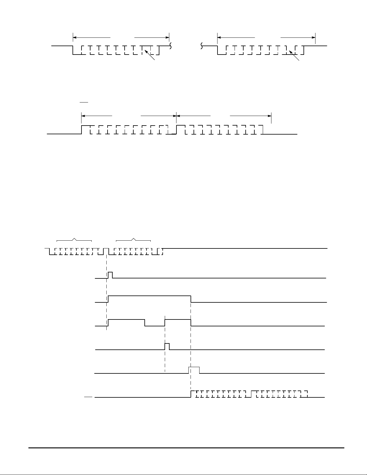
Figure 1. Data Format and Corresponding Data Position and Pins for MC14469 and MC6850
A0 to A6 = ADDRESS BITS
ID0 to ID7 = MC14469 IDENTIFICATION CODE
S0 to S7 = MC14469 STATUS CODE
D0 to D7 = ACIA BUS BITS
C0 to C6 = COMMAND BITS
SP = STOP BIT
P = PARITY BIT
ST = START BIT
D7D6D5D4D3D2D1D0
S7S6S5S4S3S2S1S0
D6D5D4D3D2D1D0
C6C5C4C3C2C1C0
D7D6D5D4D3D2D1D0
ID7ID6ID5ID4ID3ID2ID1ID0
PIN DESIGNATION
MC6850
PIN DESIGNATION
MC14469
TRANSMIT DATA (TRO
)
RECEIVE DATA (RI)
D6D5D4D3D2D1D0
A6A5A4A3A2A1A0
PIN DESIGNATION
MC6850
PIN DESIGNATION
MC14469
STATUSINPUT DATA
SPPST
SPPST
COMMAND
IDENTIFIER
(LOW LOGIC LEVEL)
COMMAND
SPPST
ADDRESS
IDENTIFIER
(HIGH LOGIC LEVEL)
ADDRESS
SPPST
S
P
S
M
S
B
Figure 2. Typical Receive/Send Cycle
TRANSMIT OUT
(TRO
)
STATUSID
SEND INPUT
(SEND)
COMMAND STROBE
OUTPUT (CS)
INTERNAL SEND
ENABLE LATCH
(SEL)
INTERNAL VALID
ADDRESS LATCH
(VAL)
VALID ADDRESS PULSE
(VAP)
S
P
X
S
3 7654210T3 765421
M
S
B
P
XXXXXXXPXXXXXX
XXXXXXX
XXXXXXX
S
T
S
T
RECEIVER INPUT (RI)
COMMANDADDRESS
M
S
B
M
S
B
S
P
S
P
76543210
76543210
P
P
T 0
X
X
Page 5

MC14469MOTOROLA
5
PIN DESCRIPTIONS
A0 – A6
Address Inputs
These inputs are the address setting pins which contain
the address match for the received signal. Pins A0 – A6 have
on–chip pull–up resistors.
C0 – C6
Command Word
These pins are the readout of the general–purpose command word which is the second word of the received signal.
CS
Command Strobe
This is the output for the command strobe signifying a valid
set of command data (C0 – C6). The pulse width is one oscillator cycle. For example, when a 307.2 kHz ceramic resonator is used, the pulse width is approximately 3 µs.
ID0 – ID7
Input Data Pins
These pins contain the input data for the first eight bits of
data to be transmitted. Pins ID0 – ID7 have on–chip pull–up
resistors.
OSC1, OSC2
Oscillator Input and Oscillator Output
These pins are t he o scillator input and o utput ( see
Figure 3).
RESET
Reset
When this pin is pulled low for a minimum of 700 ns, the
circuit is reset and ready for operation.
RI
Receive Input
This is the receive input pin.
S0 – S7
Second or Status Input Data
These pins contain the input data for the second eight bits
of data to be transmitted.
SEND
Send
This pin accepts the send command after receipt of an
address.
TRO
Transmit Register Output Signal
This pin transmits the outgoing signal. Note that it is inverted from the incoming signal. It must go through one
stage of inversion if it is to drive another MC14469.
VAP
Valid Address Pulse
This is the output for the valid address pulse upon receipt
of a matched incoming address.
V
DD
Positive Power Supply
This pin is the package positive power supply connection.
This pin may range from + 4.5 V to + 18 V with respect to
VSS.
V
SS
Negative Power Supply
This pin is the negative power supply connection. Normally
this pin is system ground.
OPERATING CHARACTERISTICS
The receipt o f a start bit on t he receive i nput (RI) line
causes the receive clock to start at a frequency equal to that
of the oscillator divided by 64. All received data is strobed in
at the center of a receive clock period. The start bit is followed by eight data bits. Seven of the bits are compared
against states of the address of the particular circuit (A0 –
A6). Address is latched 31 clock cycles after the end of the
start bit of the incoming address. The eighth bit signifies an
address word “1” or a command word “0”. Next, a parity bit is
received and checked by the internal logic for even parity.
Finally a stop bit is received. At the completion of the cycle if
the address matches, a valid address pulse (VAP) occurs.
Immediately following the address word, a command word is
received. It also contains a start bit, eight data bits, even parity bit, and a stop bit. The eight data bits are composed of a
seven–bit command, and a “0” which indicates a command
word. At the end of the command word a command strobe
pulse (CS) occurs.
A positive transition on the send input initiates the transmit
sequence. Send must occur within seven bit times of CS.
Again the transmitted data is made up of two eleven–bit
words, i.e., address and command words. The data portion
of the first word is made up from input data inputs (ID0 –
ID7), and the data for the second word from second input
data (S0 – S7) inputs. The data on inputs ID0 – ID7 is latched
one clock before the falling edge of the start bit. The data on
inputs S0 – S7 is latched on the rising edge of the start bit.
The transmitted signal is the inversion of the received signal,
which allows the use of an inverting amplifier to drive the
lines. TRO
begins either 1/2 or 1–1/2 bit times after send, de-
pending where send occurs.
The oscillator can be crystal controlled or ceramic resonator controlled for required accuracy. OSC1 can be driven
from an external oscillator (see Figure 3).
Page 6

MC14469 MOTOROLA
6
*Motorola cannot recommend one supplier over another and
in no way suggests that this is a complete listing of ceramic
resonator suppliers.
Figure 3. Oscillator Circuit
X1 = Ceramic Resonator: 307.2 kHz ± 1 kHz for 4800 baud rate.
C1 and C2 are sized per the ceramic resonator supplier’s
recommendation.
Ceramic Resonator Suppliers:*
1. Morgan Matroc, Inc., Bedford, OH, 216/232–8600
2. Radio Materials Co., Attica, IN, 317/762–2491
15 M
Ω
X1
C2
C1
NOTE: For externally generated clock,
drive OSC1, float OSC2.
OSC2OSC1
MC14469
INTERNAL
OSCILLATOR
TRORI
1.0 k
Ω
DATA LINE
GROUND LINE
MC14469
V
DATA
V
DD
V
SS
1.0 µF
Figure 4. Rectified Power from Data Lines Circuit
END
CONVERSION
ANALOG
INPUTS
8–CHANNEL A/D
CONVERTER ASSEMBLY
DIGITAL
OUTPUTS
SELECT
CHANNEL,
START
CONVERSION
CHANNEL
SELECT
MC14469
S7
S6
S5
S4
S3
S2
S1
S0
SEND
CS
C2
C1
C0
Figure 5. A–D Converter Interface
Page 7

MC14469MOTOROLA
7
Figure 6. Single Line, Simplex Data Transmission
A6,ID6
A5,ID5
A4,ID4
A3,ID3
A2,ID2
A1,ID1
A6,ID6
A5,ID5
A4,ID4
A3,ID3
A2,ID2
A1,ID1
A0,ID0
ADDRESS
0000000
S7
S7
S7
ID7
ID7
ID7
TRO
TRO
TRO
CS
CS
CS
REMOTE MC14469
STATIONS
ADDRESS
1111111
ADDRESS
0000001
TRO
10 k
10 k
10 k
SEND
RI
SEND
RI
SEND
RI
MC14469
127
MC14469
1
MC14469
0
MASTER
STATION
MC6850
ACIA
OR
UART
TRO
RI
10 k
1 k
V+
NOTE: For simplex operation the ID7 must be tied high, S7 must be tied
low, and the 7–bit ID must be the same as the 7–bit address (or set
to some unused address) to prevent erroneous responses.
V
SS
V
SS
V
DD
V
DD
V
DD
V
SS
V
SS
A6
A5
A4
A3
A2
A1
A0
A6
A5
A4
A3
A2
A1
TRO
TRO
TRO
REMOTE MC14469 STATIONS
ADDRESS
0000000
ADDRESS
1111111
ADDRESS
0000001
TRO
1 k
10 k
10 k
10 k
V
DD
SEND
VAP
V
SS
RI
V
DD
SEND
VAP
V
SS
RI
V
DD
SEND
VAP
V
SS
RI
MC14469
127
MC14469
1
MC14469
0
V
DD
MASTER
STATION
MC6850
ACIA
OR
UART
V
SS
TRO
RI
10 k
1 k
V+
Figure 7. Double Line, Full Duplex Data Transmission
Page 8

MC14469 MOTOROLA
8
N
Y
Figure 8. Flow Chart of MC14469 Operation
RESET VAL
AND SEL
LATCH
STATUS
TRANSMIT
STATUS
TRANSMIT
ID
INITIALIZE
TRANSMITTER
RESET
Y
N
Y
N
N
PREVIOUS
TRANSMISSION
COMPLETE?
SEL
SET?
SEND
=1?
Y
N
Y
RESET
SEL
ISSUE
CS
LATCH
COMMAND
COMMAND
VALID?
SEL
SET?
CLEAR COMMAND LATCH
RESET SEL
VAL
SET?
N
Y
Y
N
N
N
N
Y
Y
8 BIT
TIMES?
SET
SEL
ISSUE
VAP
SET
VAL
ADDRESS
VALID?
VAL
SET?
MSB
= 1?
INITIALIZE RECEIVER
RESET VAL
Y
RESET
Page 9

MC14469MOTOROLA
9
PACKAGE DIMENSIONS
P SUFFIX
PLASTIC DIP
CASE 711–03
NOTES:
1. POSITIONAL TOLERANCE OF LEADS (D), SHALL
BE WITHIN 0.25 (0.010) AT MAXIMUM MATERIAL
CONDITION, IN RELATION TO SEATING PLANE
AND EACH OTHER.
2. DIMENSION L TO CENTER OF LEADS WHEN
FORMED PARALLEL.
3. DIMENSION B DOES NOT INCLUDE MOLD FLASH.
1 20
40 21
B
A
C
SEATING
PLANE
DFGH
K
N
M
J
L
DIM MIN MAX MIN MAX
INCHESMILLIMETERS
A 51.69 52.45 2.035 2.065
B 13.72 14.22 0.540 0.560
C 3.94 5.08 0.155 0.200
D 0.36 0.56 0.014 0.022
F 1.02 1.52 0.040 0.060
G 2.54 BSC 0.100 BSC
H 1.65 2.16 0.065 0.085
J 0.20 0.38 0.008 0.015
K 2.92 3.43 0.115 0.135
L 15.24 BSC 0.600 BSC
M 0 15 0 15
N 0.51 1.02 0.020 0.040
_ _ _ _
Page 10

MC14469 MOTOROLA
10
FN SUFFIX
PLCC PACKAGE
CASE 777–02
NOTES:
1. DATUMS –L–, –M–, AND –N– ARE DETERMINED
WHERE TOP OF LEAD SHOULDER EXITS
PLASTIC BODY AT MOLD PARTING LINE.
2. DIMENSION G1, TRUE POSITION TO BE
MEASURED AT DATUM –T–, SEATING PLANE.
3. DIMENSIONS R AND U DO NOT INCLUDE MOLD
FLASH. ALLOWABLE MOLD FLASH IS 0.010
(0.25) PER SIDE.
4. DIMENSIONING AND TOLERANCING PER ANSI
Y14.5M, 1982.
5. CONTROLLING DIMENSION: INCH.
6. THE PACKAGE TOP MAY BE SMALLER THAN
THE PACKAGE BOTTOM BY UP TO 0.012
(0.300). DIMENSIONS R AND U ARE
DETERMINED AT THE OUTERMOST
EXTREMES OF THE PLASTIC BODY
EXCLUSIVE OF MOLD FLASH, TIE BAR BURRS,
GATE BURRS AND INTERLEAD FLASH, BUT
INCLUDING ANY MISMATCH BETWEEN THE
TOP AND BOTTOM OF THE PLASTIC BODY.
7. DIMENSION H DOES NOT INCLUDE DAMBAR
PROTRUSION OR INTRUSION. THE DAMBAR
PROTRUSION(S) SHALL NOT CAUSE THE H
DIMENSION TO BE GREATER THAN 0.037
(0.940). THE DAMBAR INTRUSION(S) SHALL
NOT CAUSE THE H DIMENSION TO BE
SMALLER THAN 0.025 (0.635).
–N–
–L–
–M–
D
Y
D
K
V
W
144
BRK
B
Z
U
X
VIEW D–D
S
L–M
M
0.007(0.180) N
S
T
S
L–M
M
0.007(0.180) N
S
T
G1
S
L–M
S
0.010 (0.25) N
S
T
K1
F
H
S
L–M
M
0.007(0.180) N
S
T
Z
G
G1
R
A
E
J
VIEW S
C
S
L–M
M
0.007(0.180) N
S
T
S
L–M
M
0.007(0.180) N
S
T
0.004 (0.10)
–T–
SEATING
PLANE
VIEW S
DIM MIN MAX MIN MAX
MILLIMETERSINCHES
A 0.685 0.695 17.40 17.65
B 0.685 0.695 17.40 17.65
C 0.165 0.180 4.20 4.57
E 0.090 0.110 2.29 2.79
F 0.013 0.019 0.33 0.48
G 0.050 BSC 1.27 BSC
H 0.026 0.032 0.66 0.81
J 0.020 ––– 0.51 –––
K 0.025 ––– 0.64 –––
R 0.650 0.656 16.51 16.66
U 0.650 0.656 16.51 16.66
V 0.042 0.048 1.07 1.21
W 0.042 0.048 1.07 1.21
X 0.042 0.056 1.07 1.42
Y ––– 0.020 ––– 0.50
Z 2 10 2 10
G1 0.610 0.630 15.50 16.00
K1 0.040 ––– 1.02 –––
S
L–M
S
0.010 (0.25) N
S
T
S
L–M
M
0.007(0.180) N
S
T
_ _ _ _
Page 11

MC14469MOTOROLA
11
This page intentionally left blank.
Page 12

MC14469 MOTOROLA
12
Motorola reserves the right to make changes without further notice to any products herein. Motorola makes no warranty , representation or guarantee regarding
the suitability of its products for any particular purpose, nor does Motorola assume any liability arising out of the application or use of any product or circuit,
and specifically disclaims any and all liability, including without limitation consequential or incidental damages. “T ypical” parameters can and do vary in different
applications. All operating parameters, including “T ypicals” must be validated for each customer application by customer’s technical experts. Motorola does
not convey any license under its patent rights nor the rights of others. Motorola products are not designed, intended, or authorized for use as components in
systems intended for surgical implant into the body, or other applications intended to support or sustain life, or for any other application in which the failure of
the Motorola product could create a situation where personal injury or death may occur. Should Buyer purchase or use Motorola products for any such
unintended or unauthorized application, Buyer shall indemnify and hold Motorola and its officers, employees, subsidiaries, affiliates, and distributors harmless
against all claims, costs, damages, and expenses, and reasonable attorney fees arising out of, directly or indirectly, any claim of personal injury or death
associated with such unintended or unauthorized use, even if such claim alleges that Motorola was negligent regarding the design or manufacture of the part.
Motorola and are registered trademarks of Motorola, Inc. Motorola, Inc. is an Equal Opportunity/Affirmative Action Employer.
How to reach us:
USA/EUROPE: Motorola Literature Distribution; JAPAN: Nippon Motorola Ltd.; Tatsumi–SPD–JLDC, Toshikatsu Otsuki,
P.O. Box 20912; Phoenix, Arizona 85036. 1–800–441–2447 6F Seibu–Butsuryu–Center, 3–14–2 Tatsumi Koto–Ku, Tokyo 135, Japan. 03–3521–8315
MFAX: RMFAX0@email.sps.mot.com – TOUCHTONE (602) 244–6609 HONG KONG: Motorola Semiconductors H.K. Ltd.; 8B Tai Ping Industrial Park,
INTERNET: http://Design–NET.com 51 Ting Kok Road, Tai Po, N.T., Hong Kong. 852–26629298
MC14469/D
*MC14469/D*
◊
 Loading...