

Page 1
MC144112MOTOROLA
1
Advance Information
CMOS
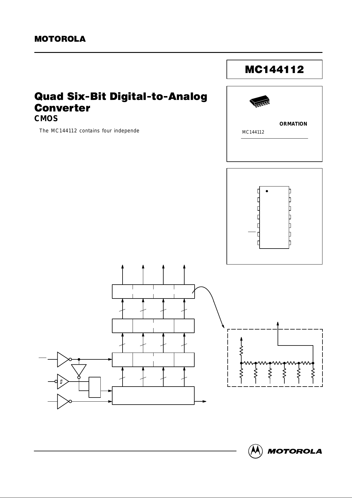
The MC144112 contains four independent DACs which are controlled
through a common serial data port. When all DACs are utilized, there are 24 bits
in the serial data stream. However, if not all DACs are utilized, the bit stream
length may be reduced by up to six bits per unused DAC.
For new designs, the MC144112 is preferred over the MC144110 and
MC144111. The newer MC144112 offers a wider operating temperature range,
lower operating supply voltage, and lower supply current.
• Operating Supply Voltage Range: 2.7 to 5.5 V
*
• Maximum Supply Current (per Package) —
All DAC Outputs = Zero: 1.25 mA @ 2.7 V
2.1 mA @ 4.5 V
All DAC Outputs = Full Scale: 30 µA @ 5.5 V
• Integral Nonlinearity: – 1
1/4 to 1/4 LSB
• Operating Temperature Range: – 40 to 85°C
• Direct R–2R Network Outputs
• Direct Interface to Motorola SPI Serial Data Port
• Digital Data Output Permits Cascading
BLOCK DIAGRAM
D
in
CLK
ENB
D
CQ
**
CLOCK
DATA
24–BIT SHIFT REGISTER
RRRRR
2R 2R 2R 2R 2R 2R
V
DD
2R
LOAD
R4 OUT
R–2R DETAIL
6
8
1
D
out
13
6 6 6 6
6 6 6 6
6 6 6 6
3 5 10 12
R1 OUT
R2 OUT
R3 OUT R4 OUT
LATCHES
INVERTING BUFFERS
R–2R LADDER NETWORKS
*This product is being evaluated for operation at supply voltages less than 2.7 V . Contact your Motorola representative for further information.
**Transparent Latch
This document contains information on a new product. Specifications and information herein are subject to change without notice.
Order this document
by MC144112/D
SEMICONDUCTOR TECHNICAL DATA
ORDERING INFORMATION
D SUFFIX
SOG PACKAGE
CASE 751A
MC1441 12D SOG Package
14
1
PIN ASSIGNMENT
11
12
13
14
8
9
105
4
3
2
1
7
6
NC
R4 Out
D
out
V
DD
CLK
NC
R3 Out
R2 Out
R1 Out
NC
D
in
V
SS
ENB
NC
NC = NO CONNECTION
Plastic DIP availability
dependent on market demand.
Motorola, Inc. 1998
REV 3
2/98 TN98030200
Page 2
MC144112 MOTOROLA
2
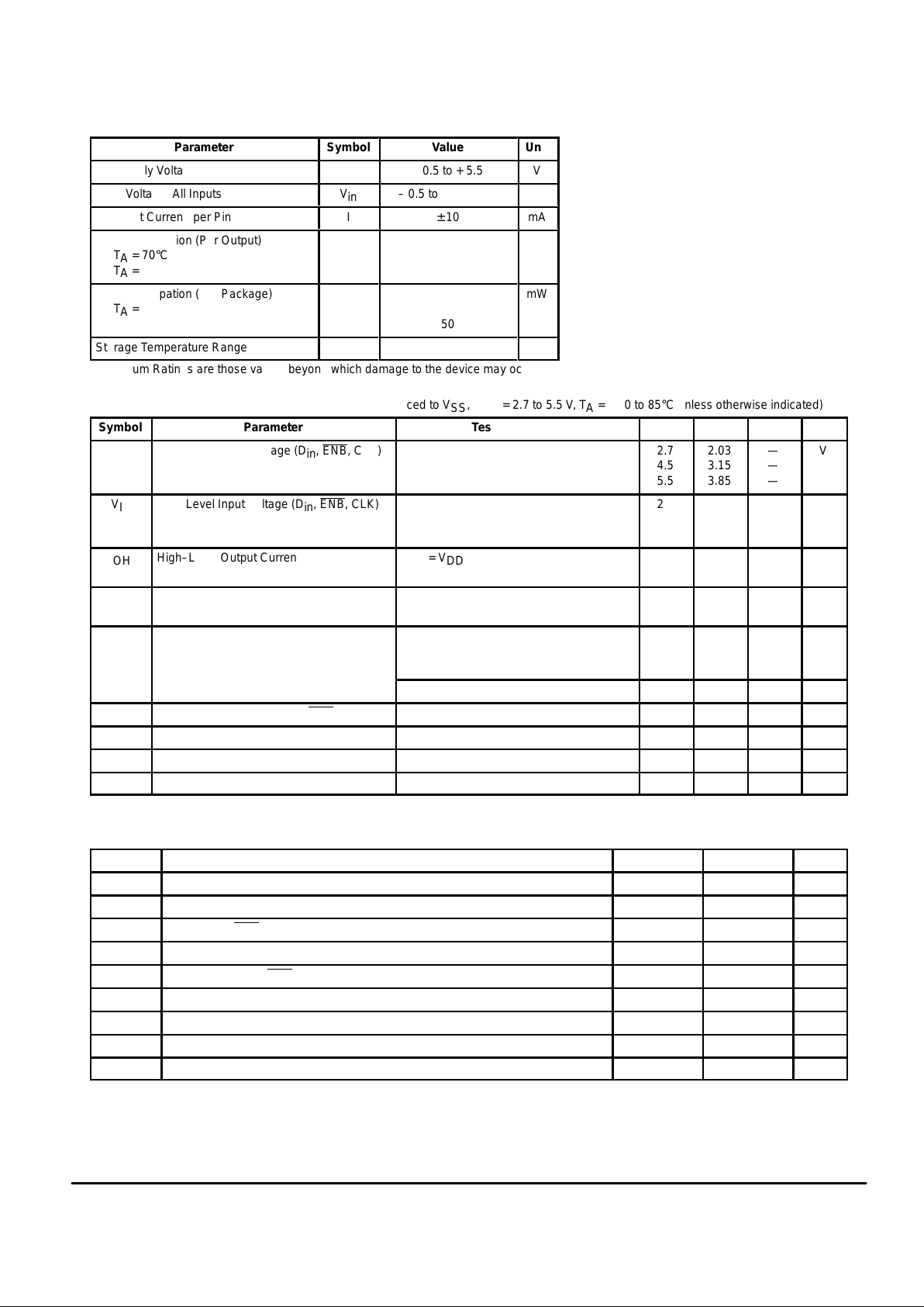
MAXIMUM RATINGS* (Voltages referenced to V
SS
)
Parameter
Symbol
Value
Unit
DC Supply Voltage
V
DD
– 0.5 to + 5.5
V
Input Voltage, All Inputs
V
in
– 0.5 to VDD + 0.5
V
DC Input Current, per Pin
I
± 10
mA
БББББББББ
Á
Power Dissipation (Per Output)
TA = 70°C
TA = 85°C
ÁÁ
Á
P
OH
БББББ
Á
50
20
Á
Á
mW
БББББББББ
Á
БББББББББ
Á
Power Dissipation (Per Package)
TA = 70°C
TA = 85°C
ÁÁ
Á
ÁÁ
Á
P
D
БББББ
Á
БББББ
Á
150
50
Á
Á
Á
Á
mW
Storage Temperature Range
T
stg
– 65 to + 150
°C
*Maximum Ratings are those values beyond which damage to the device may occur.
ELECTRICAL CHARACTERISTICS (Voltages referenced to V
SS
, VDD = 2.7 to 5.5 V , TA = – 40 to 85°C unless otherwise indicated)
Symbol
Parameter Test Conditions V
DD
Min Max Unit
V
IH
High–Level Input Voltage (Din, ENB, CLK) 2.7
4.5
5.5
2.03
3.15
3.85
—
—
—
V
V
IL
Low–Level Input Voltage (Din, ENB, CLK) 2.7
4.5
5.5
—
—
—
0.67
1.35
1.65
V
I
OH
High–Level Output Current (D
out
) V
out
= VDD – 0.5 V 2.7
4.5
0.3
1.1
—
—
mA
I
OL
Low–Level Output Current (D
out
) V
out
= 0.5 V 2.7
4.5
1.0
1.8
—
—
mA
I
SS
Quiescent Supply Current (per Package)
I
out
= 0 µA, All DAC Outputs = Zero 2.7
4.5
5.5
—
—
—
1.25
2.10
2.50
mA
I
out
= 0 µA, All DAC Outputs = Full Scale 5.5 — 30 µA
I
in
Input Leakage Current (Din, ENB, CLK) Vin = VDD or 0 V 5.5 — 1 µA
V
nonl
Integral Nonlinearity (Rn Out) See Figure 1 — – 1 1/4 1/4 LSB
V
step
Differential Nonlinearity (Rn Out) See Figure 2 — – 3/4 3/4 LSB
V
offset
Offset from V
SS
Din = $00, See Figure 1 —
1/4
1 3/4 LSB
SWITCHING CHARACTERISTICS
(VDD = 2.7 to 5.5 V , Voltages referenced to VSS, TA = – 40 to 85°C, CL = 50 pF, Input tr = tf = 20 ns unless otherwise indicated)
Symbol
Parameter Min Max Unit
t
wH
Positive Pulse Width, CLK (Figures 3 and 4) 166 — ns
t
wL
Negative Pulse Width, CLK (Figures 3 and 4) 166 — ns
t
su
Setup Time, ENB to CLK (Figures 3 and 4) 135 — ns
t
su
Setup Time, Din to CLK (Figures 3 and 4) 55 — ns
t
h
Hold Time, CLK to ENB (Figures 3 and 4) 135 — ns
t
h
Hold Time, CLK to Din (Figures 3 and 4) 55 — ns
tr, t
f
Input Rise and Fall Times, CLK — 100 µs
C
in
Input Capacitance — 10 pF
f
clk
Serial Data Clock Frequency (Refer to twH and twL Above) (Figures 3 and 4) dc 3 MHz
This device contains protection circuitry to
guard against damage due to high static
voltages or electric fields; however, it is advised that precautions be taken to avoid
application of voltage higher than maximum
rated voltages to this high–impedance circuit.
For proper operation it is recommended that
Vin and V
out
be constrained to the range VSS ≤
(Vin or V
out
) ≤VDD.
Unused inputs must always be tied to an
appropriate logic voltage level (e.g., either V
SS
or VDD).
Page 3

MC144112MOTOROLA
3
LINEARITY ERROR (integral nonlinearity). A measure of how
straight a device’s transfer function is, it indicates the worst–case
deviation of linearity of the actual transfer function from the best–
fit straight line. It is normally specified in parts of an LSB.
Figure 1. D/A Transfer Function
100
75
50
25
0
0
$00
15
$0F
31
$1F
47
$2F
63
$3F
V
nonl
PROGRAM STEP
OUTPUT VOL TAGE @ Rn Out, % (V
DD
– V
SS
)
V
offset
ACTUAL
IDEAL
Figure 2. Definition of Step Size Variance (Differential Nonlinearity)
VRn
OUT
V
step
DIGITAL NUMBER
V
step
=
± 0.75
V
DD
64
V
DD
64
(For any adjacent pair of digital numbers)
Page 4

MC144112 MOTOROLA
4
Figure 3. Serial Input, Positive Clock
D
in
D1 – MSB D
2
D
N
C
2
C
1
C
N
ENB
CLK
t
su
t
wH
t
wL
t
h
t
h
t
su
50%
50%
1 / f
clk
Figure 4. Serial Input, Negative Clock
D
in
D
2
D
N
C
2
C
1
C
N
ENB
CLK
t
su
t
wL
t
wH
t
h
t
h
t
su
D1 – MSB
1 / f
clk
Page 5

MC144112MOTOROLA
5
PIN DESCRIPTIONS
INPUTS
D
in
Data Input
Four 6–bit words are entered serially, MSB first, into the
digital data input, Din.
The last 6–bit word shifted in determines the output level of
pin R1 Out. The next–to–last 6–bit word affects pin R2 Out,
etc.
ENB
Negative Logic Enable
The ENB
pin must be low (active) during the serial load.
On the low–to–high transition of ENB
, data contained in the
shift register is loaded into the latch.
CLK
Shift Register Clock
Data is shifted into the register on the high–to–low transition of CLK. CLK is fed into the D–input of a transparent
latch, which is used for inhibiting the clocking of the shift register when ENB
is high.
The MC144112 usually uses 24 CLK cycles. See Table 1
for additional information.
OUTPUTS
D
out
Data Output
The digital data output is primarily used for cascading the
DACs and may be fed into Din of the next stage.
If not used, the output should be floated.
R1 Out through R4 Out
Resistor Network Outputs
These are the R–2R resistor network outputs. These outputs may be fed to high–impedance loads. The R value of
the resistor network ranges from 7 to 15 kΩ.
If not used, an output should be floated.
SUPPLY PINS
V
SS
Negative Supply Voltage
This pin is usually ground.
V
DD
Positive Supply Voltage
The voltage applied to this pin determines the analog output swing. The DAC output voltage range is from approximately VSS to VDD.
APPLICATIONS INFORMATION
For those applications where supply current is critical, any
unused DAC channels should be programmed for full–scale
output. The unused outputs are floated (no connects).
For example, with a 4.5 V supply, the worst case current
when all DACs are programmed for zero output is 2.1 mA.
This is 2.1 mA for the package; each DAC is drawing 1/4 of
this, or 525 µA. If only two channels are needed, minimum
supply current is achieved by programming the two unused
channels to full–scale output (all ones). In this case, the
worst case supply current is approximately two times
525 µA, or 1.05 mA.
Table 1. Number of Channels vs Clocks Required
Number of
Channels
Required
Minimum
Number of
Clock Cycles*
Outputs Used
1 6 R1 Out
2 12 R1 Out, R2 Out
3 18 R1 Out, R2 Out, R3 Out
4 24 R1 Out, R2 Out, R3 Out, R4 Out
*Additional clock cycles can be used, with the leading extra bits being don’t cares.
For example, eight clocks can be used if one channel is needed. The first two bits
are don’t cares; the last six bits determine the DAC output.
Page 6

MC144112 MOTOROLA
6
P ACKAGE DIMENSIONS
D SUFFIX
SOG (SMALL OUTLINE GULL–WING) PACKAGE
CASE 751A–03
MIN MINMAX MAX
MILLIMETERS INCHES
DIM
A
B
C
D
F
G
J
K
M
P
R
8.55
3.80
1.35
0.35
0.40
0.19
0.10
0
°
5.80
0.25
8.75
4.00
1.75
0.49
1.25
0.25
0.25
7
°
6.20
0.50
0.337
0.150
0.054
0.014
0.016
0.008
0.004
0
°
0.299
0.010
0.344
0.157
0.068
0.019
0.049
0.009
0.009
7
°
0.244
0.019
1.27 BSC 0.050 BSC
NOTES:
1. DIMENSIONING AND TOLERANCING PER ANSI
Y14.5M, 1982.
2. CONTROLLING DIMENSION: MILLIMETER.
3. DIMENSIONS A AND B DO NOT INCLUDE
MOLD PROTRUSION.
4. MAXIMUM MOLD PROTRUSION 0.15 (0.006)
PER SIDE.
5. DIMENSION D DOES NOT INCLUDE DAMBAR
PROTRUSION. ALLOWABLE DAMBAR
PROTRUSION SHALL BE 0.127 (0.005) TOTAL
IN EXCESS OF THE D DIMENSION AT
MAXIMUM MATERIAL CONDITION.
-A-
-B- P
G
C
K
SEATING
PLANE
D 14 PL
M
J
7 PL
R X 45°
1
7
814
0.25 (0.010) T B A
M
S S
B0.25 (0.010)
M M
F
Motorola reserves the right to make changes without further notice to any products herein. Motorola makes no warranty, representation or guarantee regarding
the suitability of its products for any particular purpose, nor does Motorola assume any liability arising out of the application or use of any product or circuit, and
specifically disclaims any and all liability, including without limitation consequential or incidental damages. “T ypical” parameters which may be provided in Motorola
data sheets and/or specifications can and do vary in different applications and actual performance may vary over time. All operating parameters, including “Typicals”
must be validated for each customer application by customer’s technical experts. Motorola does not convey any license under its patent rights nor the rights of
others. Motorola products are not designed, intended, or authorized for use as components in systems intended for surgical implant into the body, or other
applications intended to support or sustain life, or for any other application in which the failure of the Motorola product could create a situation where personal injury
or death may occur. Should Buyer purchase or use Motorola products for any such unintended or unauthorized application, Buyer shall indemnify and hold Motorola
and its officers, employees, subsidiaries, affiliates, and distributors harmless against all claims, costs, damages, and expenses, and reasonable attorney fees
arising out of, directly or indirectly, any claim of personal injury or death associated with such unintended or unauthorized use, even if such claim alleges that
Motorola was negligent regarding the design or manufacture of the part. Motorola and are registered trademarks of Motorola, Inc. Motorola, Inc. is an Equal
Opportunity/Affirmative Action Employer.
Mfax is a trademark of Motorola, Inc.
How to reach us:
USA/EUROPE/ Locations Not Listed: Motorola Literature Distribution; JAPAN: Nippon Motorola Ltd.: SPD, Strategic Planning Office, 141,
P.O. Box 5405, Denver, Colorado 80217. 1–303–675–2140 or 1–800–441–2447 4–32–1 Nishi–Gotanda, Shagawa–ku, Tokyo, Japan. 03–5487–8488
Mfax: RMFAX0@email.sps.mot.com – TOUCHTONE 1–602–244–6609 ASIA/PACIFIC: Motorola Semiconductors H.K. Ltd.; 8B Tai Ping Industrial Park,
Moto rola Fax Bac k System – US & Canada ONLY 1–800–774–1848 51 Ting Kok Road, Tai Po, N.T., Hong Kong. 852–26629298
– http://sps.motorola.com/mfax/
HOME PAGE: http://motorola.com/sps/ CUSTOMER FOCUS CENTER: 1–800–521–6274
MC144112/D
◊
 Loading...