

Page 1
MC144110•MC144111MOTOROLA
1
CMOS LSI
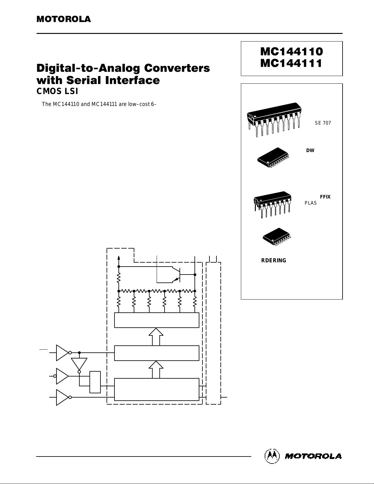
The MC144110 and MC144111 are low–cost 6–bit D/A converters with serial
interface ports to provide communication with CMOS microprocessors and
microcomputers. The MC144110 contains six static D/A converters; the
MC144111 contains four converters.
Due to a unique feature of these DACs, the user is permitted easy scaling of
the analog outputs of a system. Over a 5 to 15 V supply range, these DACs may
be directly interfaced to CMOS MPUs operating at 5 V.
• Direct R–2R Network Outputs
• Buffered Emitter–Follower Outputs
• Serial Data Input
• Digital Data Output Facilitates Cascading
• Direct Interface to CMOS µP
• Wide Operating Voltage Range: 4.5 to 15 V
• Wide Operating Temperature Range: 0 to 85°C
• Software Information is Contained in Document M68HC11RM/AD
BLOCK DIAGRAM
*Transparent Latch
D
in
CLK
ENB
D
C Q
*
C
D
6–BIT SHIFT REGISTER
HEX LATCH
HEX BUFFER (INVERTING)
D
out
Qn
OUTRnOUT
R R R R R
2R 2R 2R 2R 2R 2R
R1 OUT
V
DD
Q1 OUT
2R
C
Order this document
by MC144110/D
SEMICONDUCTOR TECHNICAL DATA
P SUFFIX
PLASTIC DIP
CASE 707
DW SUFFIX
SOG PACKAGE
CASE 751D
ORDERING INFORMATION
MC144110P Plastic DIP
MC144110DW SOG Package
P SUFFIX
PLASTIC DIP
CASE 646
DW SUFFIX
SOG PACKAGE
CASE 751G
MC144110
MC144111
MC144111P Plastic DIP
MC144111DW SOG Package
18
1
20
1
14
1
16
1
Motorola, Inc. 1995
REV 1
8/95
Page 2

MC144110•MC144111 MOTOROLA
2
PIN ASSIGNMENTS
MC144110P
R2 Out
R1 Out
Q1 Out
D
in
V
SS
ENB
R3 Out
Q3 Out
Q2 Out Q6 Out
R6 Out
D
out
V
DD
CLK
Q4 Out
R4 Out
Q5 Out
R5 Out
14
15
16
17
18
10
11
12
13
5
4
3
2
1
9
8
7
6
11
12
13
14
8
9
105
4
3
2
1
7
6
13
14
15
16
9
10
11
125
4
3
2
1
8
7
6
NC
5
4
3
2
1
10
9
8
7
6
14
15
16
17
18
19
20
11
12
13
MC144110DW
MC144111P MC144111DW
NC
R2 Out
R1 Out
Q1 Out
D
in
V
SS
ENB
R3 Out
Q3 Out
Q2 Out
Q6 Out
R6 Out
D
out
V
DD
CLK
Q4 Out
R4 Out
Q5 Out
R5 Out
R2 Out
R1 Out
Q1 Out
D
in
V
SS
ENB
Q2 Out
Q4 Out
R4 Out
D
out
V
DD
CLK
Q3 Out
R3 Out
NC
R2 Out
R1 Out
Q1 Out
D
in
V
SS
ENB
Q2 Out
Q4 Out
R4 Out
D
out
V
DD
CLK
Q3 Out
R3 Out
NC
NC = NO CONNECTION
Page 3
MC144110•MC144111MOTOROLA
3
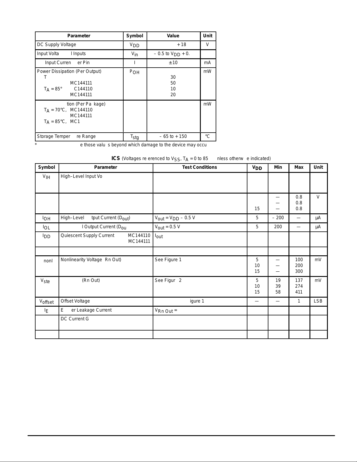
MAXIMUM RATINGS* (Voltages referenced to V
SS
)
Parameter
Symbol
Value
Unit
DC Supply Voltage
V
DD
– 0.5 to + 18
V
Input Voltage, All Inputs
V
in
– 0.5 to VDD + 0.5
V
DC Input Current, per Pin
I
± 10
mA
Power Dissipation (Per Output)
TA = 70°C, MC144110
MC144111
TA = 85°C, MC144110
MC144111
P
OH
30
50
10
20
mW
Power Dissipation (Per Package)
TA = 70°C, MC144110
MC144111
TA = 85°C, MC144110
MC144111
P
D
100
150
25
50
mW
Storage Temperature Range
T
stg
– 65 to + 150
°C
*Maximum Ratings are those values beyond which damage to the device may occur.
ELECTRICAL CHARACTERISTICS (Voltages referenced to V
SS
, TA = 0 to 85°C unless otherwise indicated)
Symbol
Parameter Test Conditions V
DD
Min Max Unit
V
IH
High–Level Input Voltage (Din, ENB, CLK) 5
10
15
3.0
3.5
4
—
—
—
V
V
IL
Low–Level Input Voltage (Din, ENB, CLK) 5
10
15
—
—
—
0.8
0.8
0.8
V
I
OH
High–Level Output Current (D
out
) V
out
= VDD – 0.5 V 5 – 200 — µA
I
OL
Low–Level Output Current (D
out
) V
out
= 0.5 V 5 200 — µA
I
DD
Quiescent Supply Current MC144110
MC144111
I
out
= 0 µA 15
15
—
—
12
8
mA
I
in
Input Leakage Current (Din, ENB, CLK) Vin = VDD or 0 V 15 — ± 1 µA
V
nonl
Nonlinearity Voltage (Rn Out) See Figure 1 5
10
15
—
—
—
100
200
300
mV
V
step
Step Size (Rn Out) See Figure 2 5
10
15
19
39
58
137
274
411
mV
V
offset
Offset Voltage from V
SS
Din = $00, See Figure 1 — — 1 LSB
I
E
Emitter Leakage Current VRn
Out
= 0 V 15 — 10 µA
h
FE
DC Current Gain IE = 0.1 to 10.0 mA
TA = 25°C
— 40 — —
V
BE
Base–to–Emitter Voltage Drop IE = 1.0 mA — 0.4 0.7 V
This device contains protection circuitry to
guard against damage due to high static
voltages or electric fields; however, it is advised that precautions be taken to avoid
application of voltage higher than maximum
rated voltages to this high–impedance circuit.
For proper operation it is recommended that
Vin and V
out
be constrained to the range VSS ≤
(Vin or V
out
) ≤VDD.
Unused inputs must always be tied to an
appropriate logic voltage level (e.g., either V
SS
or VDD).
Page 4

MC144110•MC144111 MOTOROLA
4
SWITCHING CHARACTERISTICS
(Voltages referenced to VSS, TA = 0 to 85°C, CL = 50 pF, Input tr = tf = 20 ns unless otherwise indicated)
Symbol
Parameter V
DD
Min Max Unit
t
wH
Positive Pule Width, CLK (Figures 3 and 4) 5
10
15
2
1.5
1
—
—
—
µs
t
wL
Negative Pulse Width, CLK (Figure 3 and 4) 5
10
15
5
3.5
2
—
—
—
µs
t
su
Setup Time, ENB to CLK (Figures 3 and 4) 5
10
15
5
3.5
2
—
—
—
µs
t
su
Setup Time, Din to CLK (Figures 3 and 4) 5
10
15
1000
750
500
—
—
—
ns
t
h
Hold Time, CLK to ENB (Figures 3 and 4) 5
10
15
5
3.5
2
—
—
—
µs
t
h
Hold Time, CLK to Din (Figures 3 and 4) 5
10
15
5
3.5
2
—
—
—
µs
tr, t
f
Input Rise and Fall Times 5 – 15 — 2 µs
C
in
Input Capacitance 5 – 15 — 7.5 pF
LINEARITY ERROR (integral linearity). A measure of how
straight a device’s transfer function is, it indicates the worst–case
deviation of linearity of the actual transfer function from the best–
fit straight line. It is normally specified in parts of an LSB.
Figure 1. D/A Transfer Function
100
75
50
25
0
0
$00
15
$0F
31
$1F
47
$2F
63
$3F
V
nonl
PROGRAM STEP
OUTPUT VOLTAGE @ Rn Out, % (V
DD
– V
SS
)
V
offset
ACTUAL
IDEAL
Page 5

MC144110•MC144111MOTOROLA
5
Figure 2. Definition of Step Size
VRn
OUT
STEP
SIZE
DIGITAL NUMBER
Step Size =
± 0.75
V
DD
64
V
DD
64
(For any adjacent pair of digital numbers)
Figure 3. Serial Input, Positive Clock
D
in
D
1
D
2
D
N
C
2
C
1
C
N
ENB
CLK
t
su
t
wH
t
wL
t
h
t
h
t
su
50%
50%
Figure 4. Serial Input, Negative Clock
D
in
D
1
D
2
D
N
C
2
C
1
C
N
ENB
CLK
t
su
t
wL
t
wH
t
h
t
h
t
su
Page 6

MC144110•MC144111 MOTOROLA
6
PIN DESCRIPTIONS
INPUTS
D
in
Data Input
Six–bit words are entered serially, MSB first, into digital
data input, Din. Six words are loaded into the MC144110
during each D/A c ycle; four w ords a re loaded into the
MC144111.
The last 6–bit word shifted in determines the output level of
pins Q1 Out and R1 Out. The next–to–last 6–bit word affects
pins Q2 Out and R2 Out, etc.
ENB
Negative Logic Enable
The ENB pin must be low (active) during the serial load.
On the low–to–high transition of ENB
, data contained in the
shift register is loaded into the latch.
CLK
Shift Register Clock
Data is shifted into the register on the high–to–low transition of CLK. CLK is fed into the D–input of a transparent
latch, which is used for inhibiting the clocking of the shift register when ENB
is high.
The number of clock cycles required for the MC144110 is
usually 36. The MC144111 usually uses 24 cycles. See
Table 1 for additional information.
OUTPUTS
D
out
Data Output
The digital data output is primarily used for cascading the
DACs and may be fed into Din of the next stage.
R1 Out through Rn Out
Resistor Network Outputs
These are the R–2R resistor network outputs. These outputs may be fed to high–impedance input FET op amps to
bypass the on–chip bipolar transistors. The R value of the resistor network ranges from 7 to 15 kΩ.
Q1 Out through Qn Out
NPN Transistor Outputs
Buffered DAC outputs utilize an emitter–follower configuration for current–gain, thereby allowing interface to low–impedance circuits.
SUPPLY PINS
V
SS
Negative Supply Voltage
This pin is usually ground.
V
DD
Positive Supply Voltage
The voltage applied to this pin is used to scale the analog
output swing from 4.5 to 15 V p–p.
Table 1. Number of Channels vs Clocks Required
Number of
Channels
Required
Number of
Clock Cycles
Outputs Used on MC144110 Outputs Used on MC144111
1 6 Q1/R1 Q1/R1
2 12 Q1/R1, Q2/R2 Q1/R1, Q2/R2
3 18 Q1/R1, Q2/R2, Q3/R3 Q1/R1, Q2/R2, Q3/R3
4 24 Q1/R1, Q2/R2, Q3/R3, Q4/R4 Q1/R1, Q2/R2, Q3/R3, Q4/R4
5 30 Q1/R1, Q2/R2, Q3/R3, Q4/R4, Q5/R5 Not Applicable
6 36 Q1/R1, Q2/R2, Q3/R3, Q4/R4, Q5/R5, Q6/R6 Not Applicable
Page 7

MC144110•MC144111MOTOROLA
7
PACKAGE DIMENSIONS
P SUFFIX
PLASTIC DIP
CASE 707–02
MIN MINMAX MAX
MILLIMETERS INCHES
DIM
22.22
6.10
3.56
0.36
1.27
1.02
0.20
2.92
23.24
6.60
4.57
0.56
1.78
1.52
0.30
3.43
0
°
0.51
0.875
0.240
0.140
0.014
0.050
0.040
0.008
0.115
0.915
0.260
0.180
0.022
0.070
0.060
0.012
0.135
15
°
1.02
2.54 BSC
7.62 BSC
0.100 BSC
0.300 BSC
0
°
0.020
15
°
0.040
A
B
C
D
F
G
H
J
K
L
M
N
NOTES:
1. POSITIONAL TOLERANCE OF LEADS (D),
SHALL BE WITHIN 0.25 (0.010) AT MAXIMUM
MATERIAL CONDITION, IN RELATION TO
SEATING PLANE AND EACH OTHER.
2. DIMENSION L TO CENTER OF LEADS WHEN
FORMED PARALLEL.
3. DIMENSION B DOES NOT INCLUDE MOLD
FLASH.
1 9
1018
B
A
H
F
G
D
SEATING
PLANE
N
K
M
J
L
C
DW SUFFIX
SOG PACKAGE
CASE 751D–04
NOTES:
1. DIMENSIONING AND TOLERANCING PER
ANSI Y14.5M, 1982.
2. CONTROLLING DIMENSION: MILLIMETER.
3. DIMENSIONS A AND B DO NOT INCLUDE
MOLD PROTRUSION.
4. MAXIMUM MOLD PROTRUSION 0.150
(0.006) PER SIDE.
5. DIMENSION D DOES NOT INCLUDE
DAMBAR PROTRUSION. ALLOWABLE
DAMBAR PROTRUSION SHALL BE 0.13
(0.005) TOTAL IN EXCESS OF D DIMENSION
AT MAXIMUM MATERIAL CONDITION.
–A–
–B–
20
1
11
10
S
A
M
0.010 (0.25) B
S
T
D20X
M
B
M
0.010 (0.25)
P10X
J
F
G
18X
K
C
–T–
SEATING
PLANE
M
R
X 45
_
DIM MIN MAX MIN MAX
INCHESMILLIMETERS
A 12.65 12.95 0.499 0.510
B 7.40 7.60 0.292 0.299
C 2.35 2.65 0.093 0.104
D 0.35 0.49 0.014 0.019
F 0.50 0.90 0.020 0.035
G 1.27 BSC 0.050 BSC
J 0.25 0.32 0.010 0.012
K 0.10 0.25 0.004 0.009
M 0 7 0 7
P 10.05 10.55 0.395 0.415
R 0.25 0.75 0.010 0.029
_ _
_ _
Page 8

MC144110•MC144111 MOTOROLA
8
P SUFFIX
PLASTIC DIP
CASE 646–06
NOTES:
1. LEADS WITHIN 0.13 (0.005) RADIUS OF TRUE
POSITION AT SEATING PLANE AT MAXIMUM
MATERIAL CONDITION.
2. DIMENSION L TO CENTER OF LEADS WHEN
FORMED PARALLEL.
3. DIMENSION B DOES NOT INCLUDE MOLD
FLASH.
4. ROUNDED CORNERS OPTIONAL.
1 7
14 8
B
A
F
H G D
K
C
N
L
J
M
SEATING
PLANE
DIM MIN MAX MIN MAX
MILLIMETERSINCHES
A 0.715 0.770 18.16 19.56
B 0.240 0.260 6.10 6.60
C 0.145 0.185 3.69 4.69
D 0.015 0.021 0.38 0.53
F 0.040 0.070 1.02 1.78
G 0.100 BSC 2.54 BSC
H 0.052 0.095 1.32 2.41
J 0.008 0.015 0.20 0.38
K 0.115 0.135 2.92 3.43
L 0.300 BSC 7.62 BSC
M 0 10 0 10
N 0.015 0.039 0.39 1.01
_ _ _ _
DW SUFFIX
SOG PACKAGE
CASE 751G–02
DIM MIN MAX MIN MAX
INCHESMILLIMETERS
A 10.15 10.45 0.400 0.411
B 7.40 7.60 0.292 0.299
C 2.35 2.65 0.093 0.104
D 0.35 0.49 0.014 0.019
F 0.50 0.90 0.020 0.035
G 1.27 BSC 0.050 BSC
J 0.25 0.32 0.010 0.012
K 0.10 0.25 0.004 0.009
M 0 7 0 7
P 10.05 10.55 0.395 0.415
R 0.25 0.75 0.010 0.029
M
B
M
0.010 (0.25)
NOTES:
1. DIMENSIONING AND TOLERANCING PER ANSI
Y14.5M, 1982.
2. CONTROLLING DIMENSION: MILLIMETER.
3. DIMENSIONS A AND B DO NOT INCLUDE MOLD
PROTRUSION.
4. MAXIMUM MOLD PROTRUSION 0.15 (0.006) PER
SIDE.
5. DIMENSION D DOES NOT INCLUDE DAMBAR
PROTRUSION. ALLOWABLE DAMBAR
PROTRUSION SHALL BE 0.13 (0.005) TOTAL IN
EXCESS OF D DIMENSION AT MAXIMUM
MATERIAL CONDITION.
–A–
–B– P8X
G14X
D16X
SEATING
PLANE
–T–
S
A
M
0.010 (0.25) B
S
T
16 9
81
F
J
R
X 45
_
_ _ _ _
M
C
K
Motorola reserves the right to make changes without further notice to any products herein. Motorola makes no warranty, representation or guarantee regarding
the suitability of its products for any particular purpose, nor does Motorola assume any liability arising out of the application or use of any product or circuit,
and specifically disclaims any and all liability, including without limitation consequential or incidental damages. “T ypical” parameters can and do vary in different
applications. All operating parameters, including “T ypicals” must be validated for each customer application by customer’s technical experts. Motorola does
not convey any license under its patent rights nor the rights of others. Motorola products are not designed, intended, or authorized for use as components in
systems intended for surgical implant into the body, or other applications intended to support or sustain life, or for any other application in which the failure of
the Motorola product could create a situation where personal injury or death may occur. Should Buyer purchase or use Motorola products for any such
unintended or unauthorized application, Buyer shall indemnify and hold Motorola and its officers, employees, subsidiaries, affiliates, and distributors harmless
against all claims, costs, damages, and expenses, and reasonable attorney fees arising out of, directly or indirectly, any claim of personal injury or death
associated with such unintended or unauthorized use, even if such claim alleges that Motorola was negligent regarding the design or manufacture of the part.
Motorola and are registered trademarks of Motorola, Inc. Motorola, Inc. is an Equal Opportunity/Affirmative Action Employer.
How to reach us:
USA/EUROPE: Motorola Literature Distribution; JAPAN: Nippon Motorola Ltd.; Tatsumi–SPD–JLDC, Toshikatsu Otsuki,
P.O. Box 20912; Phoenix, Arizona 85036. 1–800–441–2447 6F Seibu–Butsuryu–Center, 3–14–2 Tatsumi Koto–Ku, Tokyo 135, Japan. 03–3521–8315
MFAX: RMFAX0@email.sps.mot.com – TOUCHTONE (602) 244–6609 HONG KONG: Motorola Semiconductors H.K. Ltd.; 8B Tai Ping Industrial Park,
INTERNET: http://Design–NET.com 51 Ting Kok Road, Tai Po, N.T., Hong Kong. 852–26629298
MC144110/D
*MC144110/D*
◊
 Loading...