

Page 1
Device
Operating
Temperature Range
Package
SEMICONDUCTOR
TECHNICAL DATA
OPERATIONAL AMPLIFIERS
ORDERING INFORMATION
MC1436CD,D
MC1436CP1,P1
TA = 0° to +70°C
SO–8
Plastic DIP
(Top View)
PIN CONNECTIONS
Order this document by MC1436/D
D SUFFIX
PLASTIC PACKAGE
CASE 751
(SO–8)
P1 SUFFIX
PLASTIC PACKAGE
CASE 626
1
1
8
8
N.C.
V
CC
Output
Offset Null
Offset Null
1
2
3
4
8
7
6
5
Noninv. Input
V
EE
Inv. Input
+
1
MOTOROLA ANALOG IC DEVICE DATA
The MC1436, C was designed for use as a summing amplifier, integrator,
or amplifier with operating characteristics as a function of the external
feedback components.
• Output Voltage Swing:
±22 V
pk(min)
(VCC = +28 V, VEE = –28 V)
• Fast Slew Rate: 2.0 V/µs Typ
• Internally Compensated
• Offset Voltage Null Capability
• Input Overvoltage Protection
• A
VOL
: 500,000 Typ
• Characteristics Independent of Power Supply Voltages:
(±5.0 Vdc to ±36 Vdc)
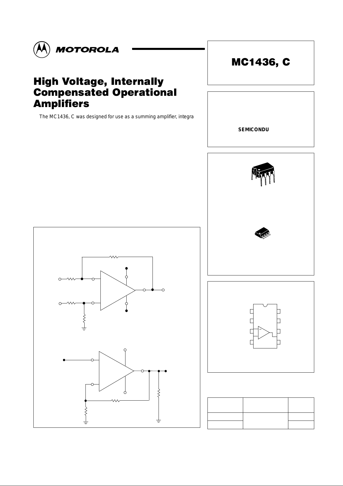
Figure 1. Differential Amplifier with ±20 V
Common Mode Input Voltage Range
Figure 2. Typical Noninverting X10 Voltage Amplifier
MC1436 , C
2
3
4
6
7
+28 V
VO = 10 (VB –VA)
R4
4.7 k
R2
100 k
R1
10 k
R3
470
V
A
V
B
+
–
–28 V
MC1436 , C
3
7 +28 V
6
4 –28 V
1.0 k
2
VO = 44 V
pp
VI = 4.4 V
pp
RL
≥
5.0 k
9.0 k
+
_
Motorola, Inc. 1996 Rev 5
Page 2
MC1436, C
2
MOTOROLA ANALOG IC DEVICE DATA
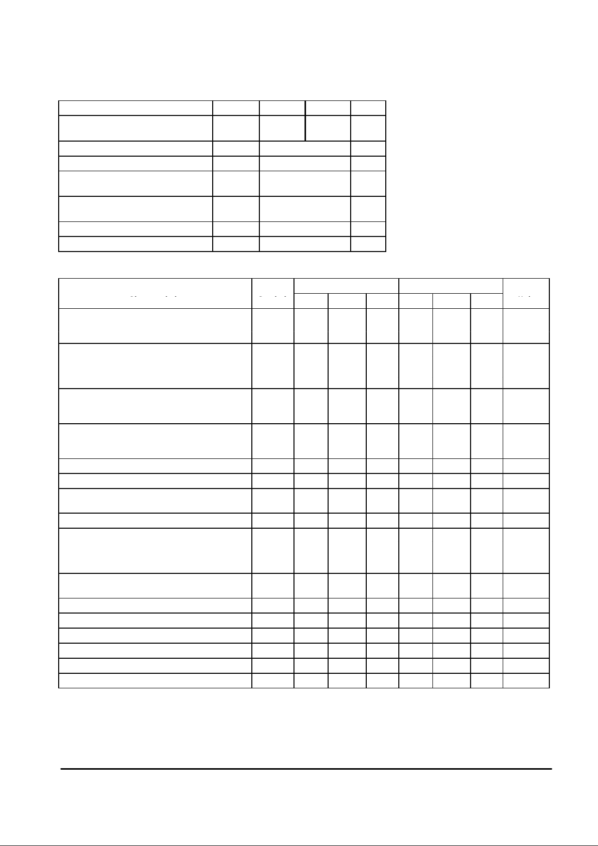
MAXIMUM RATINGS (T
A
= +25°C, unless otherwise noted.)
Rating Symbol MC1436 MC1436C Unit
Power Supply Voltage V
CC
V
EE
+34
–34
+30
–30
Vdc
Input Differential Voltage Range V
IDR
Note 2 V
Input Common Mode Voltage Range V
ICR
Note 2 V
Output Short Circuit Duration
(VCC = VEE = 28 Vdc, VO = 0)
t
SC
5.0 sec
Power Dissipation (Package Limitation)
Derate above TA = +25°C
P
D
680
4.6
mW
mW/°C
Operating Ambient Temperature Range T
A
0 to +70 °C
Storage Temperature Range T
stg
–65 to +150 °C
ELECTRICAL CHARACTERISTICS (V
CC
= +28 V , VEE = –28 V , TA = 25°C, unless otherwise noted.)
MC1436 MC1436C
Characteristic Symbol
Min Typ Max Min Typ Max
Unit
Input Bias Current I
IB
nAdc
TA = +25°C – 15 40 – 25 90
TA = T
low
to T
high
(See Note 1) – – 55 – – –
Input Offset Current I
IO
nAdc
TA = +25°C – 5.0 10 – 10 25
TA = +25°C to T
high
– – 14 – – –
TA = T
low
to +25°C – – 14 – – –
Input Offset Voltage V
IO
mVdc
TA = +25°C – 5.0 10 – 5.0 12
TA = T
low
to T
high
– – 14 – – –
Differential Input Impedance (Open loop, f ≤ 5.0 Hz) MΩ
Parallel Input Resistance rp – 10 – – 10 – pF
Parallel Input Capacitance Cp – 2.0 – – 2.0 –
Common Mode Input Impedance (f ≤ 5.0 Hz) z
ic
– 250 – – 250 – MΩ
Input Common Mode Voltage Range V
ICR
±22 ±25 – ±18 ±20 – Vpk
Equivalent Input Noise Voltage e
n
nV/(Hz)1/
2
(AV = 100, RS = 10 kΩ, f = 1.0 kHz, BW = 1.0 Hz) – 50 – – 50 –
Common Mode Rejection (DC) CMR 70 110 – 50 90 – dB
Large Signal DC Open Loop Voltage Gain A
VOL
V/V
(VO = ±10 V, RL = 100 kΩ)TA = +25°C 70,000 500,000 – 50,000 500,000 –
TA = T
low
to T
high
50,000 – – – – –
(VO = ±10 V, RL = 10 kΩ, TA = +25°C) – 200,000 – – 200,000 –
Power Bandwidth (Voltage Follower) BWp kHz
(AV = 1, RL = 5.0 kΩ, THD ≤ 5%, VO = 40 Vpp) – 23 – – 23 –
Unity Gain Crossover Frequency (Open loop) f
c
– 1.0 – – 1.0 – MHz
Phase Margin (Open loop, Unity Gain) φ
m
– 50 – – 50 – Degrees
Gain Margin A
M
– 18 – – 18 – dB
Slew Rate (Unity Gain) SR – 2.0 – – 2.0 – V/µs
Output Impedance (f ≤ 5.0 Hz) z
O
– 1.0 – – 1.0 – kΩ
Short Circuit Output Current I
SC
– ±17 – – ±19 – mAdc
NOTES: 1. T
low
= 0°C for MC1436,C T
high
= +70°C for MC1436,C
2.Either or both input voltages must not exceed the magnitude of VCC or VEE +3.0 V .
Page 3
MC1436, C
3
MOTOROLA ANALOG IC DEVICE DATA
ELECTRICAL CHARACTERISTICS (V
CC
= +28 V , VEE = –28 V , TA = 25°C, unless otherwise noted.)
Characteristic Unit
MC1436CMC1436
Symbol
Characteristic UnitMaxTypMinMaxTypMinSymbol
Output Voltage Range (RL = 5.0 kΩ) V
O
V
pk
VCC = +28 Vdc, VEE = –28 Vdc ±20 ±22 – ±20 ±22 –
VCC = +36 Vdc, VEE = –36 Vdc – – – – – –
Power Supply Rejection µV/V
VEE = Constant, Rs ≤ 10 kΩ PSR + – 35 200 – 50 –
VCC = Constant, Rs ≤ 10 kΩ PSR – – 35 200 – 50 –
Power Supply Current (See Note 2) I
CC
I
EE
–
–
2.6
2.6
5.0
5.0
–
–
2.6
2.6
5.0
5.0
mAdc
DC Quiescent Power Consumption (VO = 0) P
C
– 146 280 – 146 280 mW
NOTES: 2. VCC = VEE = 5.0 Vdc to 30 Vdc for MC1436
VCC = VEE = 5.0 Vdc to 28 Vdc for MC1436C
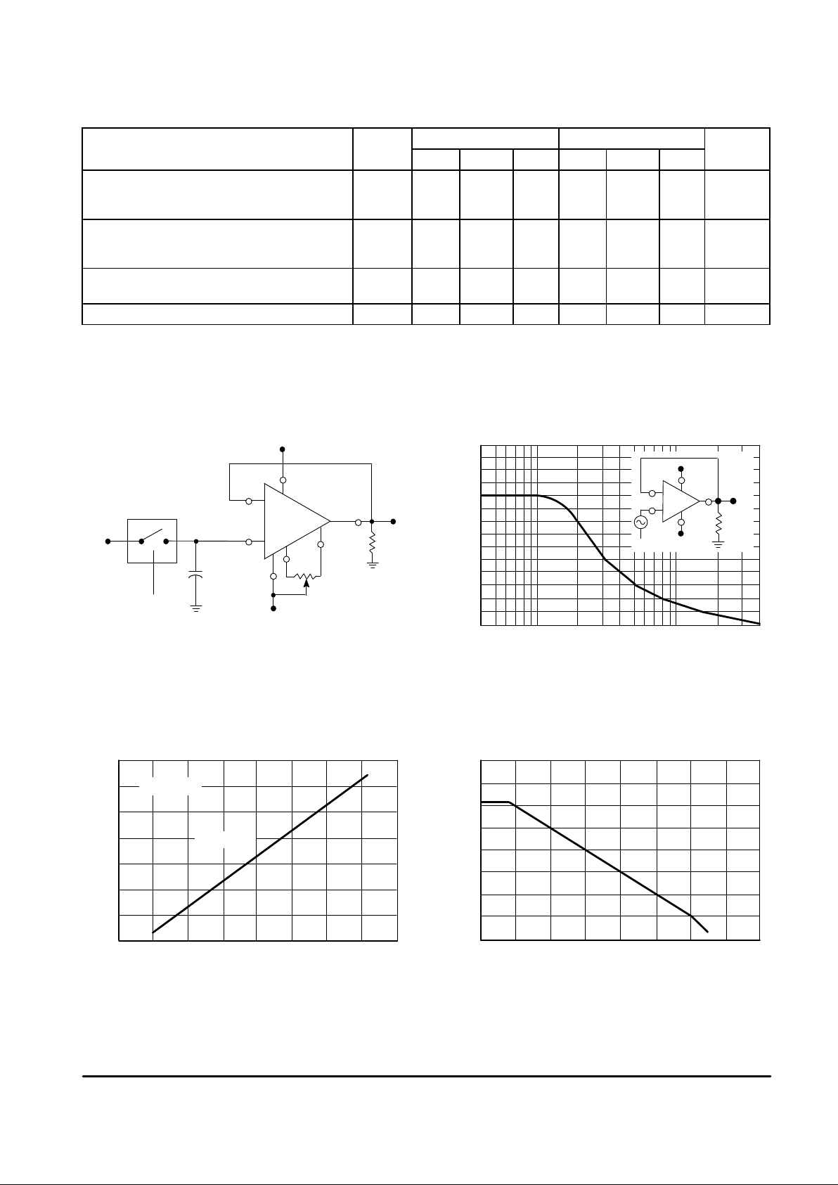
Figure 3. Low–Drift Sample and Hold Figure 4. Power Bandwidth
Figure 5. Peak Output Voltage Swing versus
Power Supply Voltage
Figure 6. Open Loop Frequency Response
Switch
Sample
Command
1.0
µ
F
Polycarbonate
–28 V
1
10 k
5
6
*e
o
+28 V
2
3
e
i
*Drift due to bias current
is typically 8.0 mV s
7
4
MC1436
+
–
f, FREQUENCY (kHz)
70
60
50
40
30
20
10
0
4.0 6.0 8.0 10 20 40 60 80 100 200 400
2
3
7
+28 V
V
O
10 k
–28 V
6
4
V
O
, OUTPUT VOLTAGE (V )
p–p
VCC/VEE, POWER SUPPLY VOLTAGE (Vdc)
V , OUTPUT VOLTAGE SWING (V )
O
35
30
25
20
15
10
5.0
0
0 10 20 30 40
RL = 5.0 k
Ω
TA = 25° C
f, FREQUENCY (kHz)
A , VOLTAGE GAIN (dB)
VOL
140
120
100
80
60
40
20
0
–20
1.0 10 100 1.0 k 10 k 100 k 1.0 M 10 M 100 M
pk
Page 4

MC1436, C
4
MOTOROLA ANALOG IC DEVICE DATA
Figure 7. Output Short Circuit Current
versus Temperature
Figure 8. Input Bias Current
versus Temperature
TA, AMBIENT TEMPERATURE (°C)
I , OUTPUT SHORT CIRCUIT CURRENT (mAdc)
SC
32
28
24
20
16
12
8.0
4.0
0
–75 –50 –25 0 25 50 75 100 125
Sink
Source
I , INPUT BIAS CURRENT (NORMALIZED)
IB
3.2
2.8
2.4
2.0
1.6
1.2
0.8
0.4
0
–75 –50 –25 0 25 50 75 100 125
TA, AMBIENT TEMPERATURE (
°
C)
Figure 9. Inverting Feedback Model Figure 10. Noninverting Feedback Model
Figure 11. Audio Amplifier
Ao ( ω ) E
X
Z
1
I
in
V
in
V
1
(+)
R
3
V2 3
E
X
V
O
z
o
Z
2
–
+
6
I
O
R
L
z
o
zo = z
o
1 +Z2/Z
1
Ao (
ω
)
If : Ao ( ω )
∞
V
O
V
i
= –
Z
2
Z
1
If : R3 Ơ Z
1
zi
Z
1
z
i
(–)
2
+
–
z
i
z
i
Z
1
+
–
z
o
I
O
R
L
V
O
6
z
o
E
X
V
in
3
(+)
I
i
Z
3
Z
2
z
i
(–)
zi = , zi Very High
2
Ao ( ω ) E
X
zo = z
o
1 +Z2/Z
1
Ao (
ω
)
Ao ( ω ) Z
1
1 +Z2/Z
1
∞
V
O
V
i
= 1 +Z2/Z1, when AO (ω)
+
–
Zo
³
0
Ao (
ω) ³ ∞
0.1 µF
10 µF
D
1
D
2
D
3
R
L
0.24
0.24
4.7
2N3716
or Equiv
2N3766
of Equiv
2N3740
or Equiv
2N3791
or Equiv
Current Drain,
ID
100 mAdc @
R1 = 51
Ω
D1 , D2 , D3 =
1N4001
Common
Heat Sink
VO = 48 Vpp
PO = 72 W (rms) @ RL = 4.0
Ω
PO = 36 W (rms) @ RL = 8.0
Ω
VCC = +30 Vdc
50 µF
+
2
3
10 k
0.5
µ
F
V
i
10 k
10
µ
F
–
+
MC1536
51
7
4
1.0 k
1.0 k
R1
1.0 k
1.0 k
10
µ
F
+
6
VEE = –30 Vdc
100 k
Page 5

MC1436, C
5
MOTOROLA ANALOG IC DEVICE DATA
Figure 12. Voltage Controlled Current Source or Transconductance Amplifier
with 0 V to 40 V Compliance
Figure 13. Representative Schematic Diagram
Figure 14. Equivalent Circuit
V
EE
V
CC
Inverting
Noninverting
2
3
4
Offset Adjust
–
+
–
+
6
7
Z
in
10 k
51
V
O
R
out
V
i
AV
in
I
R
TC
–
+
MC1436,C
6
4
–6.0 V
3
2
+50 V
7
R
TC
510
–V
i
I
O
= 2.0 mA/V
V
i
=
ZO =
R1RTC (R3 +R4)
R1 (RTC +R3) – R2 R4
R1
100 k
R2
100 k
R3
100 k
R4
100 k
1
–
+
7
V
CC
2
3
Input
Input
6.0 k
1.5 k
7.7 k
1.0 k
39 k
1.0 k
50
500
5.0 k
Output
22
26
15 k
28 k
200
7.0 k
39 k
35 pF
4.7 k
3.5 k
12 k 1.2k
Offset Adjust
6
7.0 k
39 k
500 500
1.5 k
1.5 k 1.0 k
28 k
77 k
5
Page 6

MC1436, C
6
MOTOROLA ANALOG IC DEVICE DATA
OUTLINE DIMENSIONS
NOTES:
1. DIMENSION L TO CENTER OF LEAD WHEN
FORMED PARALLEL.
2. PACKAGE CONTOUR OPTIONAL (ROUND OR
SQUARE CORNERS).
3. DIMENSIONING AND TOLERANCING PER ANSI
Y14.5M, 1982.
14
58
F
NOTE 2
–A–
–B–
–T–
SEATING
PLANE
H
J
G
D
K
N
C
L
M
M
A
M
0.13 (0.005) B
M
T
DIM MIN MAX MIN MAX
INCHESMILLIMETERS
A 9.40 10.16 0.370 0.400
B 6.10 6.60 0.240 0.260
C 3.94 4.45 0.155 0.175
D 0.38 0.51 0.015 0.020
F 1.02 1.78 0.040 0.070
G 2.54 BSC 0.100 BSC
H 0.76 1.27 0.030 0.050
J 0.20 0.30 0.008 0.012
K 2.92 3.43 0.115 0.135
L 7.62 BSC 0.300 BSC
M ––– 10 ––– 10
N 0.76 1.01 0.030 0.040
__
D SUFFIX
PLASTIC PACKAGE
CASE 751–05
(SO–8)
ISSUE R
P1 SUFFIX
PLASTIC PACKAGE
CASE 626–05
ISSUE K
SEATING
PLANE
1
4
58
A0.25MCB
SS
0.25MB
M
h
q
C
X 45
_
L
DIM MIN MAX
MILLIMETERS
A 1.35 1.75
A1 0.10 0.25
B 0.35 0.49
C 0.18 0.25
D 4.80 5.00
E
1.27 BSCe
3.80 4.00
H 5.80 6.20
h
0 7
L 0.40 1.25
q
0.25 0.50
__
NOTES:
1. DIMENSIONING AND TOLERANCING PER ASME
Y14.5M, 1994.
2. DIMENSIONS ARE IN MILLIMETERS.
3. DIMENSION D AND E DO NOT INCLUDE MOLD
PROTRUSION.
4. MAXIMUM MOLD PROTRUSION 0.15 PER SIDE.
5. DIMENSION B DOES NOT INCLUDE MOLD
PROTRUSION. ALLOWABLE DAMBAR
PROTRUSION SHALL BE 0.127 TOTAL IN EXCESS
OF THE B DIMENSION AT MAXIMUM MATERIAL
CONDITION.
D
E
H
A
B
e
B
A1
C
A
0.10
Page 7

MC1436, C
7
MOTOROLA ANALOG IC DEVICE DATA
Motorola reserves the right to make changes without further notice to any products herein. Motorola makes no warranty , representation or guarantee regarding
the suitability of its products for any particular purpose, nor does Motorola assume any liability arising out of the application or use of any product or circuit, and
specifically disclaims any and all liability, including without limitation consequential or incidental damages. “T ypical” parameters which may be provided in Motorola
data sheets and/or specifications can and do vary in different applications and actual performance may vary over time. All operating parameters, including “Typicals”
must be validated for each customer application by customer’s technical experts. Motorola does not convey any license under its patent rights nor the rights of
others. Motorola products are not designed, intended, or authorized for use as components in systems intended for surgical implant into the body, or other
applications intended to support or sustain life, or for any other application in which the failure of the Motorola product could create a situation where personal injury
or death may occur. Should Buyer purchase or use Motorola products for any such unintended or unauthorized application, Buyer shall indemnify and hold Motorola
and its officers, employees, subsidiaries, affiliates, and distributors harmless against all claims, costs, damages, and expenses, and reasonable attorney fees
arising out of, directly or indirectly, any claim of personal injury or death associated with such unintended or unauthorized use, even if such claim alleges that
Motorola was negligent regarding the design or manufacture of the part. Motorola and are registered trademarks of Motorola, Inc. Motorola, Inc. is an Equal
Opportunity/Affirmative Action Employer.
Page 8

MC1436, C
8
MOTOROLA ANALOG IC DEVICE DATA
How to reach us:
USA/EUROPE/Locations Not Listed: Motorola Literature Distribution; JAP AN: Nippon Motorola Ltd.; Tatsumi–SPD–JLDC, 6F Seibu–Butsuryu–Center,
P.O. Box 20912; Phoenix, Arizona 85036. 1–800–441–2447 or 602–303–5454 3–14–2 Tatsumi Koto–Ku, Tokyo 135, Japan. 03–81–3521–8315
MFAX: RMF AX0@email.sps.mot.com – TOUCHT ONE 602–244–6609 ASIA/PACIFIC: Motorola Semiconductors H.K. Ltd.; 8B Tai Ping Industrial Park,
INTERNET: http://Design–NET.com 51 Ting Kok Road, Tai Po, N.T., Hong Kong. 852–26629298
MC1436/D
*MC1436/D*
◊
 Loading...