

Page 1
SEMICONDUCTOR TECHNICAL DATA
Order this document
by MC141541/D
CMOS
The MC141541 is a high performance HCMOS device designed to interface
with a microcontroller unit to allow colored symbols or characters to be
displayed on a color monitor. The on–chip PLL allows both multi–system
operation and self–generation of system timing. It also minimizes the MCU’s
burden through its built–in 273 bytes display/control RAM. By storing a full
screen of data and control information, this device has the capability to carry out
‘screen–refresh’ without MCU supervision.
Since there is no spacing between characters, special graphics–oriented
characters can be generated by combining two or more character blocks. There
are two different resolutions that users can choose. By changing the number of
dots per horizontal line to 320 (CGA) or 480 (EGA), smaller characters with
higher resolution can be easily achieved.
Special functions such as character bordering or shadowing, multi–level
windows, double height and double width, and programmable vertical length of
character can also be incorporated. Furthermore, neither massive information
update nor extremely high data transmission rate are expected for normal on–
screen display operation, and serial protocols are implemented in lieu of any
parallel formats to achieve minimum pin count.
A special feature, character RAM fonts, is implemented in this MOSD
enhanced version (EMOSD). Users can download their own fonts and display
them at any time once the chip is powered on. There are two ways for users to
build and store fonts. One is a conventional approach to have masked ROM
fonts. A newer approach is to store the fonts in the EPROM accessed by the
MCU and then download them into the EMOSD character RAM. With this new
technique, users have more flexibility in preparing their fonts and the effective
number of fonts is greatly increased.
• Two Selectable Resolutions: 320 (CGA) and 480 (EGA) Dots per Line
• Fully Programmable Character Array of 10 Rows by 24 Columns
• 273 Bytes Direct Mapping Display RAM Architecture
• Internal PLL Generates a Wide–Ranged System Clock
• For High–End Monitor Application, Maximum Horizontal Frequency is
110 kHz (52.8 MHz Dot Clock at 480 Mode)
• Programmable Vertical Height of Character to Meet Multi–Sync
Requirement
• Programmable Vertical and Horizontal Positioning for Display Center
• 120 Characters and Graphic Symbols ROM and Eight Programmable
Character RAM
• 10 x 16 Dot Matrix Character
• Character–by–Character Color Selection
• A Maximum of Four Selectable Colors per Row
• Double Character Height and Double Character Width
• Character Bordering or Shadowing
• Three Fully Programmable Background Windows with Overlapping
Capability
• Provides a Clock Output Synchronous to the Incoming H Sync for External
PWM
• M_BUS (IIC) Interface with Address $7A
• Single Positive 5 V Supply
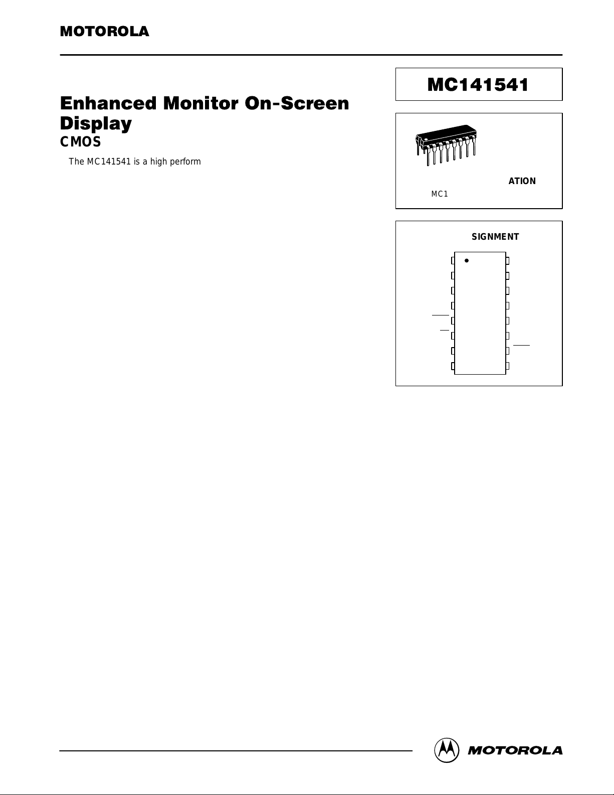
P SUFFIX
PLASTIC DIP
CASE 648
ORDERING INFORMATION
MC141541P Plastic DIP
PIN ASSIGNMENT
V
SS(A)
VCO
RP
V
)
DD(A
HFLB
SS
SDA(MOSI)
SCL(SCK)
1
2
3
4
6
7
8
16
15
14
13
125
11
10
9
V
SS
R
G
B
FBKG
HTONE/
PWMCK
VFLB
V
DD
REV 1
2/97 TN97031200
Motorola, Inc. 1997
MOTOROLA
MC141541
1
Page 2
SDA(MOSI)
SCL(SCK)
SS
VFLB
7
8
6
10
CHS
VERD
MCLK
8
DATA RECEIVER
RFG
BUS ARBITRATION
LOGIC
NROW
VERTICAL
CONTROL
CIRCUIT
BLOCK DIAGRAM
8
DATA
3
RA,CA,DA
9
ADDRC
26
Y
4
R
5
CH
4
LP
HORD
5
8
MEMORY AND DA T A
MANAGEMENT
CHARACTER ROMS/RAMS
8
ROW
BUFFER
6
CRADDR
SHADOW
26
RDATA
Z
OSD_EN
VERD
BSEN
54
15
13
CRS
WADDR
WCOLOR
AND
CONTROL
CCOLORS
AND SELECT
CHS
CWS
V
DD(A)
VSS(A)
V
DD
V
SS
RP
VCO
HFLB
4
1
9
16
MCLK
3
2
5
HORIZONTAL
CONTROL
AND PLL
54
WADDR
BACKGROUND
GENERAT OR
SC
DHOR
CCLK
5
HORD
W
3
WCOLOR
AND CONTROL
15
10
CHAR
10–BIT SHIFT
REGISTERS
OSD_EN
COLOR ENCODER
G
R
BSEN
SHADOW
LUMINANCE
B
FBKG
CWS
BLACKEDGE
13
1115 14 13 12
PWMCK
HTONE/
CCOLORS
AND SELECT
MC141541
2
MOTOROLA
Page 3
ABSOLUTE MAXIMUM RATINGS Voltage Referenced to V
Symbol
V
V
T
NOTE: Maximum Ratings are those values beyond which damage to the device may occur.
Supply Voltage – 0.3 to + 7.0 V
DD
Input Voltage VSS – 0.3 to
in
Id Current Drain per Pin Excluding V
and V
Operating Temperature Range 0 to 85 °C
Ta
Storage Temperature Range – 65 to + 150 °C
stg
Functional operation should be restricted to the limits in the Electrical Characteristics tables or Pin Description section.
Characteristic Value Unit
DD
SS
SS
V
VDD + 0.3
25 mA
This device contains circuitry to protect the
inputs against damage due to high static voltages or electric fields; however, it is advised that
normal precautions be taken to avoid applications of any voltage higher than the maximum
rated voltages to this high impedance circuit.
For proper operation it is recommended that
Vin and V
(Vin or V
be tied to an appropriate logic voltage level (e.g.,
either VSS or VDD). Unused outputs must be left
open.
be constrained to the range VSS ≤
out
) ≤ VDD. Unused inputs must always
out
AC ELECTRICAL CHARACTERISTICS (V
Symbol Characteristic Min Typ Max Unit
Output Signal (R, G, B, FBKG and HTONE/PWMCK) C
t
r
t
f
F
HFLB
DC CHARACTERISTICS V
Symbol Characteristic Min Typ Max Unit
V
OH
V
OL
V
IL
V
IH
V
IL
V
IH
V
IL
V
IH
I
II
I
II
I
DD
Figure 1
Rise Time
Fall Time
HFLB Input Frequency — — 110 kHz
= V
DD
DD(A)
High Level Output Voltage
I
= – 5 mA
out
Low Level Output Voltage
I
= 5 mA
out
Digital Input Voltage (Not Including SDA and SCL)
Logic Low
Logic High
Input Voltage of Pin SDA and SCL in SPI Mode
Logic Low
Logic High
Input Voltage of Pin SDA and SCL in M_BUS Mode
Logic Low
Logic High
High–Z Leakage Current (R, G, B and FBKG) – 10 — + 10 µA
Input Current (Not Including RP, VCO, R, G, B, FBKG and
HTONE/PWMCK)
Supply Current (No Load on Any Output) — — + 15 mA
= V
DD
= 5.0 V ± 10%, VSS = V
= 5.0 V, VSS = V
DD(A)
= 0 V, TA = 25°C, Voltage Referenced to VSS)
SS(A)
= 30 pF, see
load
= 0 V, TA = 25°C, Voltage Referenced to V
SS(A)
—
—
VDD – 0.8 — — V
— — VSS + 0.4 V
—
0.7 V
DD
—
0.7 V
DD
—
0.7 V
DD
– 10 — + 10 µA
—
—
—
—
—
—
—
—
SS
0.3 V
0.3 V
0.3 V
6
6
—
—
—
DD
DD
DD
ns
ns
V
V
V
V
V
V
MOTOROLA
90%
10%
tf tr
Figure 1. Switching Characteristics
90%
10%
MC141541
3
Page 4
PIN DESCRIPTIONS
ООООО
ООООО
ООООО
V
Analog ground for PLL operation is separated from digital
ground for optimal performance.
VCO (Pin 2)
(Pin 1)
SS(A)
This pin provides the signal ground to the PLL circuitry.
er the external R, G, and B amplifiers’ gain to achieve a
transparent windowing effect. If the PWMCK_EN bit is set to
1 via M_BUS or SPI, this pin is changed to a mode–dependent clock output with 50/50 duty cycle and is synchronous
with the input horizontal synchronization signal at Pin 5. The
frequency is dependent on the mode in which the EMOSD is
currently running. The exact frequencies in the different resolution modes are described in Table 1.
Pin 2 is a control voltage input to regulate an internal oscillator frequency . See the Application Diagram for the application values used.
RP (Pin 3)
An external RC network is used to bias an internal VCO to
resonate at the specific dot frequency . The maximum voltage
at Pin 3 should not exceed 3.5 V at any condition. See the
Application Diagram for the application values used.
V
DD(A)
(Pin 4)
Pin 4 is a positive 5 V supply for PLL circuitry . Analog power for PLL is separated from digital power for optimal performance.
(Pin 5)
HFLB
This pin inputs a negative polarity horizontal synchronize
signal pulse to phase lock an internal system clock generated by the on–chip VCO circuit.
(Pin 6)
SS
This input pin is part of the SPI serial interface. An active
low signal generated by the master device enables this slave
device to accept data. This pin should be pulled high to terminate the SPI communication. If M_BUS is employed as the
serial interface, this pin should be tied to either V
DD
or V
SS
SDA (MOSI) (Pin 7)
Data and control messages are being transmitted to this
chip from a host MCU via one of the two serial bus systems.
With either protocol, this wire is configured as a uni–directional data line. (Detailed description of these two protocols
will be discussed in the M_BUS and SPI sections).
SCL (SCK) (Pin 8)
A separate synchronizing clock input from the transmitter
is required for either protocol. Data is read at the rising edge
of each clock signal.
VDD (Pin 9)
This is the power pin for the digital logic of the chip.
(Pin 10)
VFLB
Similar to Pin 5, this pin inputs a negative polarity vertical
synchronize signal pulse.
HTONE/PWMCK (Pin 11)
This is a multiplexed pin. When the PWMCK_EN bit is
cleared after power–on or by the MCU, this pin is HTONE
and outputs a logic high during windowing except when
graphics or characters are being displayed. It is used to low-
T able 1. PWM CLK Frequency
Resolution
320 dots/line
480 dots/line
NOTE: Hf is
the frequency of the input H sync on Pin 5.
Frequency
32 x H
f
48 x H
f
Duty Cycle
50/50
50/50
Typically, this clock is fed into an external pulse width modulation module as its clock source. Because of the synchronization between PWM clock and H sync, a better
performance on the PWM controlled functions can be
achieved.
FBKG (Pin 12)
This pin outputs a logic high while displaying characters or
windows when the FBKGC bit in the frame control register is
0, and output a logic high only while displaying characters
when the FBKGC bit is 1. It is defaulted to high–impedance
state after power–on, or when there is no output. An external
10 kΩ resistor pulled low is recommended to avoid level toggling caused by hand effect when there is no output.
B,G,R (Pins 13,14,15)
EMOSD color output is TTL level RGB to the host monitor.
These three signals are active high output pins that are in a
.
high–impedance state when EMOSD is disabled.
VSS (Pin 16)
This is the ground pin for the digital logic of the chip.
SYSTEM DESCRIPTION
MC141541 is a full–screen memory architecture. Refresh
is performed by the built–in circuitry after a screenful of display data has been loaded through the serial bus. Only
changes to the display data need to be input afterward.
Serial data, which includes screen mapping address, display information, and control messages, are transmitted via
one of the two serial buses: M_BUS or SPI (mask option).
These two sets of buses are multiplexed onto a single set of
wires. Standard parts offer M_BUS transmission. Parts
which offer SPI transmission mode must be specially
manufactured as custom parts.
Data is received from the serial port and stored by the
memory management circuit. Line data is stored in a row
buffer for display and refreshing. During this storing and retrieving cycle, bus arbitration logic patrols the internal traffic
to make sure that no crashes occur between the slower serial bus receiver and the fast ‘screen–refresh’ circuitry. After
the full–screen display data is received through one of the
serial communication interfaces, the link can be terminated if
a change of the display is not required.
MC141541
4
MOTOROLA
Page 5
The bottom half of the Block Diagram contains the hardware functions for the entire system. It performs all the
EMOSD functions such as programmable vertical length
(from 16 lines to 63 lines), display clock generation (which is
phase locked to the incoming horizontal sync signal at Pin 5
), bordering or shadowing, and multiple windowing.
HFLB
COMMUNICATION PROTOCOLS
M_BUS Serial Communication
This is a two–wire serial communication link that is fully
compatible with the IIC bus system. It consists of an SDA bidirectional data line and an SCL clock input line. Data is sent
from a transmitter (master) to a receiver (slave) via the SDA
line, and is synchronized with a transmitter clock on the SCL
line at the receiving end. The maximum data rate is limited to
100 kbps and the default chip address is $7A, but is hardware changeable by mask set.
Operating Procedure
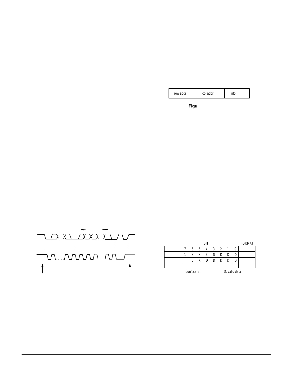
Figure 2 shows the M_BUS transmission format. The master initiates a transmission routine by generating a start
condition followed by a slave address byte. Once the address is properly identified, the slave will respond with an acknowledge signal by pulling the SDA line low during the ninth
SCL clock. Each data byte that follows must be eight bits
long, plus the acknowledge bit, for a total of nine bits. Appropriate row and column address information and display
data can be downloaded sequentially in one of the three
transmission formats described in the Data Transmission
Formats section. In the cases of no acknowlege or completion of data transfer, the master will generate a stop condition
to terminate the transmission routine. Note that the OSD_EN
bit must be set after all the display information has been sent,
in order to activate the EMOSD circuitry of MC141541 so that
the received information can be displayed.
DATA BYTES
ACK
SDA
CHIP ADDRESS
ACK
Display RAM and Control Registers
After the proper identification by the receiving device, a
data train of arbitrary length is transmitted from the master.
There are three transmission formats from (a) to (c) as stated
below. The data train in each sequence consists of row address (R), column address (C), and display information (I), as
shown in Figure 3. In format (a), display information data
must be preceded with the corresponding row address and
column address. This format is particularly suitable for updating small amounts of data between different rows. However,
if the current information byte has the same row address as
the one before, format (b) is recommended.
row addr col addr info
Figure 3. Data Packet
For a full–screen pattern change that requires a massive
information update, or during power–up, most of the row and
column addresses of either (a) or (b) formats will be consecutive. Therefore, a more efficient data transmission format (c)
should be applied. This sends the RAM starting row and column addresses once only, and then treats all subsequent
data as display information. The row and column addresses
will be automatically incremented internally for each display
information data from the starting location.
The data transmission formats are:
(a) R – > C – > I – > R – > C – > I – > . . . . . . . . .
(b) R – > C – > I – > C – > I – > C – > I. . . . . . .
(c) R – > C – > I – > I – > I – > . . . . . . . . . . . . .
T o dif ferentiate the row and column addresses when transferring data from master, the MSB (most significant bit) is set,
as in Figure 4: ‘1’ to represent row, and ‘0’ for column address. Furthermore, to distinguish the column address between formats (a), (b), and (c), the sixth bit of the column
address is set to ‘1’ which represents format (c), and ‘0’ for
format (a) or (b). However, there is some limitation on using
mixed formats during a single transmission. It is permissible
to change the format from (a) to (b), or from (a) to (c), or from
(b) to (a), but not from (c) back to (a) or (b).
SCL
1
STAR T CONDITION
9 82–7
STOP CONDITION
Figure 2. M_BUS Format
DA TA TRANSMISSION FORMATS
In this enhanced version MOSD, both display RAM, control registers, and character RAM fonts need to be programmed after power–on. The arrangement of the display
RAM and control registers is on the row–column basis, while
the character RAM is on the segment–line basis. Although
the address basis is different, the data downloading protocols are very similar and will be described in the following
sections.
MOTOROLA
ADDRESS
ROW
COLUMN
COLUMN
X: don’t care D: valid data
FORMATBIT
01234567
a, b, c
DDDDXXX1
a, b
DDDDDX00
DDDDDX10
c
Figure 4. Row & Column Address Bit Patterns
Character RAM
The structure of eight character RAM fonts is shown in Figure 5. They occupy the font number from 0 to 7. Because of
the 10 x 16 dot matrix font, each font is broken down into two
segments in the horizontal direction and 16 lines in the vertical direction. Therefore, there are five dots that need to be
defined for each specified segment–line location. This 5–bit
data forms the lower five bits of the information data byte and
the higher three bits are ignored. Because there are 16 segments (two segments per font) and 16 lines, both the segment and line addresses are four bits wide.
MC141541
5
Page 6

from (a) to (c), or from (b) to (a), but not from (c) back to (a) or
(b).
Figure 5. Segment Address Structure
Basically, the transmission format is very similar to that for
display RAM or control registers. The major difference is to
replace the row and column address with segment address
and line address, respectively. After the proper identification
by the receiving device, a data train of arbitrary length is
transmitted from the master.
There are three transmission formats, from (a) to (c) as
stated below. The data train in each sequence consists of
segment adress (S), line address (L), and font information (I),
as shown in Figure 6. In format (a), each font information
data has to be preceded with the corresponding segment address and line address. This format is particularly suitable for
updating small portions of font patterns. However, if the current information byte has the same segment address as the
one before, format (b) is recommended.
SEG ADDRESS LINE ADDRESS INFORMATION
ADDRESS
SEG
LINE
LINE
X: don’t care D: valid data
FORMATBIT
01234567
a, b, c
DDDDXX11
a, b
DDDDXX00
DDDDXX10
c
Figure 7. Segment and Line Address Bit Patterns
MEMORY MANAGEMENT
Inside this chip there are three kinds of RAM: display
RAM, control registers, and character RAM. Display RAM
and control registers are addressed with row and column
(coln) number in sequence, while the character RAM is addressed with segment and line number. The transmission
format is described in the Data Transmission Formats section. In addition to the eight RAM fonts numbered from $00 to
$07, 120 masked ROM fonts numbered from $08 to $7F are
also built in to this chip.
Display RAM and Control Registers
The spaces between Row 0 and Coln 0 to Row 9 and Coln
23 are called display registers, and each contains a character RAM/ROM number corresponding to a display location on
the monitor screen. Every data row is associated with two
control registers, located at Coln 30 and 31 of their respective rows, that control the character display format for that
row. In addition, three window control registers for each of
three windows, together with three frame control registers,
occupy the first 13 columns of Row 10.
X X X D4 D3 D2 D1 D0
NOTE: X means don’t care bit and D means valid data bit.
Figure 6. Data Packet
For a new font pattern change which requires a massive
information update, or during power–up, most of the segment
and column address on either format (a) or (b) will appear to
be redundant. A more efficient data transmission format (c)
should be applied. It sends the character RAM starting segment and line addresses only once, and then treats all subsequent data as font information. The segment and line
addresses will be automatically incremented internally for
each RAM font data from the starting location.
The data transmission formats are:
(a) S – > L– > I – > S – > L – > I – > . . . . . . . . .
(b) S – > L – > I – > L – > I – > L – > I. . . . . . .
(c) S – > L – > I – > I – > I – > . . . . . . . . . . . . .
To differentiate the segment address from row and line addresses when transferring data, Bit 7 (MSB) and Bit 6 are
set, as in Figure 7, to ‘11’ to represent segment address, or
‘00’ to represent line address in format (a) or (b), or ‘01’ to
represent line address in format (c). However, there is some
limitation on using mixed formats during a single transmission. It is permissible to change the format from (a) to (b), or
0
ROW
9
0 235689 12
10
WINDOW 1 WINDOW 2 FRAME CRTL REGWINDOW 3
WINDOW AND FRAME CONTROL REGISTERS
COLUMN
DISPLAY REGISTERS
23 24...
29 30 310
RESERVED SPACE
ROW CONTROL REGISTERS
Figure 8. Memory Map
The user should handle the internal RAM address location
with care, especially those rows with double length alphanumeric symbols. For example, if Row n is destined to be
double height on the memory map, the data displayed on
screen Rows n and n+1 will be represented by the data contained in the memory address of Row n only . The data of the
next Row n+1 on the memory map will appear on the screen
as n+2 and n+3 row space, and so on. Hence, it is not necessary to load a row of blank data to compensate for the double
row. The user should minimize excessive rows of data in
MC141541
6
MOTOROLA
Page 7

memory in order to avoid overrunning the limited amount of
Ç
Ç
row space on the screen.
For rows with double width alphanumeric symbols, only
the data contained in the even numbered columns of the
memory map are shown. Odd numbered columns are
treated in the same manner as double height rows.
Character RAM/ROM
The RAM fonts occupy the font numbers $00 to $07, and
their patterns can be changed at any time via the SPI or
M_BUS protocol. The masked ROM fonts are fixed and located from number $08 to $7F. See Figure 9 for details.
FONT NUMBER: $00 – $7F
7DA9872107E7F
. . . . . . . . . . . . . . . . . . . . . . . . . . .
8 CHARACTER RAM FONTS
($00 – $07)
120 CHARACTER ROM FONTS
($08 – $7F)
Figure 9. Arrangement of Character RAM/ROM Fonts
MOTOROLA
MC141541
7
Page 8

REGISTERS
Display Register
01234567
CCS0
CRADDR
Bit 7 CCS0 — This bit defines a specific character color
out of the two preset colors. Color 1 is selected if this bit is
cleared, and Color 2 otherwise.
Bit 6–0 CRADDR — These seven bits address the 128
characters or symbols residing in the character ROM.
Row Control Registers
Row 10 Coln 2
1234567
0
ROW 10
COLN 2
COL END ADDR
MSB LSB
RG
B
Bits 2–0 R, G and B — These bits control the color of Window 1. Window 1 occupies Columns 0–2 of Row 10; Window
2 occupies Columns 3–5; and Window 3 occupies Columns
6–8. Window 1 has the highest priority, and Window 3 the
least. If window overlapping occurs, the higher priority window will cover the lower one, and the higher priority color will
take over on the overlap window area. If the start address is
greater than the end address, this window will not be displayed.
Coln 30
01234567
COLN 30
CWSCHSB2G2R2B1G1R1
Bits 7–2 — Color 1 is determined by R1, G1, and B1; Color
2 by R2, G2, and B2.
Bit 1 CHS — This bit determines the height of a display
symbol. When it is set, the symbol is displayed in double
height.
Bit 0 CWS — Bit 0 is similar to Bit 1; when this bit is set, the
character is displayed in double width.
Coln 31
01234567
COLN 31
B4G4R4B3G3R3
Bits 7–2 — Color 3 is determined by R3, G3, and B3; Color
4 by R4, G4, and B4.
Window 1 Registers
Row 10 Coln 0
1234567
0
ROW 10
COLN 0
ROW START ADDR
MSB
LSB
ROW END ADDR
MSB
LSB
Window 2 Registers
Row 10 Coln 3
1234567
0
ROW 10
COLN 3
ROW START ADDR
MSB
LSB
ROW END ADDR
MSB LSB
Row 10 Coln 4
1234567
0
ROW 10
COLN 4
COL START ADDR
MSB LSB
WEN CCS1
VPOL
Bit 2 WEN — This bit enables the background Window 2
generation when it is set.
Bit 1 CCS1 — This additional color select bit provides the
characters residing within Window 2 with two extra color
selections, making a total of four selections for that row.
Bit 0 VPOL — This bit selects the polarity of the incoming
vertical sync signal (VFLB
) on Pin 5. If it is negative polarity,
clear this bit. Otherwise, set this bit to 1 to represent the positive V sync signal. After power–on, this bit is cleared.
Row 10 Coln 5
1234567
0
ROW 10
COLN 5
COL END ADDR
MSB LSB
RG
B
Row 10 Coln 1
1234567
0
ROW 10
COLN 1
COL START ADDR
MSB
LSB
WEN CCS1
HPOL
Bit 2 WEN — This bit enables the background Window 1
generation when it is set.
Bit 1 CCS1 — This additional color select bit provides the
characters residing within Window 1 with two extra color
selections, making a total of four selections for that row.
Bit 0 HPOL — This bit selects the polarity of the incoming
horizontal sync signal (HFLB
) on Pin 5. If it is negative polarity, clear this bit. Otherwise, set this bit to 1 to represent the
positive H sync signal. After power–on, this bit is cleared.
MC141541
8
Bit 2–0 R, G and B — These bits control the color of Window 2. Window 1 occupies Columns 0–2 of Row 10; Window
2 occupies Columns 3–5; and Window 3 occupies Columns
6–8. Window 1 has the highest priority, and Window 3 the
least. If window overlapping occurs, the higher priority window will cover the lower one, and the higher priority color will
take over on the overlap window area. If the start address is
greater than the end address, this window will not be displayed.
Window 3 Registers
Row 10 Coln 6
1234567
0
ROW 10
COLN 6
ROW START ADDR
MSB
LSB
ROW END ADDR
MSB
LSB
MOTOROLA
Page 9

Row 10 Coln 7
ОООООООООООО
1234567
0
ROW 10
COLN 7
COL START ADDR
MSB
LSB
WEN CCS1
PWMCK_EN
Bit 2 WEN — This bit enables the background Window 3
generation when it is set.
Bit 1 CCS1 — This additional color select bit provides the
characters residing within Window 3 with two extra color
selections, making a total of four selections for that row.
Bit 0 PWMCK_EN — When this bit is set to 1, the HTONE/
PWMCK pin will be switched to a clock output which is synchronous to the H sync and used as an external PWM (pulse
width modulation) clock source. Refer to the pin description
of HTONE/PWMCK for more information. After power–on,
the default value is 0.
Row 10 Coln 8
1234567
0
ROW 10
COLN 8
COL END ADDR
MSB
RG
LSB
B
Bit 2–0 R, G and B — These bits control the color of Window 3. Window 1 occupies Columns 0–2 of Row 10; Window
2 occupies Columns 3–5; and Window 3 occupies 6–8. Window 1 has the highest priority , and Window 3 the least. If window overlapping occurs, the higher priority window will cover
the lower one, and the higher priority color will take over on
the overlap window area. If the start address is greater than
the end address, this window will not be displayed.
Bit 7 TB — Reserved test bit.
Bit 6 TB — Reserved test bit.
Bit 5–0 CH5–CH0 — These six bits determine the displayed character height. It is possible to have a proper character height by setting a value greater than or equal to 16 on
a different horizontal frequency monitor. Setting a value below 16 will not have a predictable result. Figure 10 illustrates
how this chip expands the built–in character font to the desired height.
0
1
2
3
4
5
6
7
8
9
10
11
12
13
14
15
Built–in font Display character
(10x16 matrix)
when CH=16
16 lines 22 lines
when CH=22
34 lines25 lines
Frame Control Registers
Frame Control Register Row 10 Coln 9
1234567
0
COLN 9
MSB
VERTD
LSB
Bit 7–0 VERTD — These eight bits define the vertical starting position. There are a total of 256 steps, with an increment
of four horizontal lines per step for each field. The value cannot be zero anytime, and the default value is 4.
Frame Control Register Row 10 Coln 10
01234567
COLN 10
TB
MSB
HORD
LSB
Bit 7 TB — Reserved test bit.
Bit 6–0 HORD — These bits define the horizontal starting
position for character display. Seven bits give a total of 96
steps and each increment represents a five–dot shift to the
right on the monitor screen. The value cannot be zero anytime, and the default value is 10.
Frame Control Register Row 10 Coln 11
6543 210
7
COLN 11
TB TB
CH5 CH4 CH3 CH2 CH1 CH0
Display character
Display character
when CH=34when CH=25
Figure 10. Variable Character Height
Frame Control Register Row 10 Coln 12
COLN 12
7
OSD_EN
65
BSEN SHADOW FBKGCX32BTB TB
43
2
1
0
Bit 7 OSD_EN — The OSD circuit is activated when this bit
is set.
Bit 6 BSEN — This bit enables the character bordering or
shadowing function when it is set.
Bit 5 SHADOW — Characters with black–edge shadowing
are selected if this bit is set; otherwise bordering prevails.
Bit 4 TB — Reserved test bit.
Bit 3 X32B — This bit determines the number of dots per
horizontal line. There are 320 dots per horizontal line if Bit
X32B is clear, which is also the default power–on state.
Otherwise, 480 dots per horizontal sync line is chosen when
Bit X32B is set to 1. Refer to Table 2 for details.
Bit 2 TB — Reserved test bit.
Bit 1 TB — Reserved test bit.
Bit 0 FBKGC — Bit 0 determines the configuration of the
FBKG output pin. When it is clear, the FBKG pin outputs high
while displaying characters or windows; otherwise, the
FBKG pin outputs high only while displaying characters.
MOTOROLA
MC141541
9
Page 10

T able 2. Resolution Setting
Ï
Ï
Register Setting (32B)
Dot Number per H Sync Line
ООООООООО
0
320
ÎÎ
1
480
Î
vertical delay =
VERTD x 4 + 1 H scan lines
VFLB
variable number of H scan lines
10
11
12
13
14
15
0
1
2
3
4
5
6
7
8
9
Bordering
10
11
12
13
14
15
0
1
2
3
4
5
6
7
8
9
Shadowing
Figure 11. Character Bordering and Shadowing
Frame Format and Timing
Figure 12 illustrates the positions of all display characters
on the screen relative to the leading edge of horizontal and
vertical flyback signals. The shaded area indicates the area
outside the “safe viewing area” for the display characters.
Notice that there are two components in the equations stated
in Figure 12 for horizontal and vertical delays: fixed delays
from the leading edge of HFLB
and VFLB signals, regardless
of the values of HORD and VERTD (47 dots + phase detection pulse width) and one H scan line for horizontal and vertical delays, respectively; and variable delays determined by
the values of HORD and VERTD. Refer to Frame Control
Registers Coln 9 and 10 for the definitions of VERTD and
HORD.
Phase detection pulse width is a function of the external
charge–up resistor, which is the 330 kΩ resistor in a series
with 2 kΩ to VCO pin in the Application Diagram. Dot frequency is determined by the equation
X32B is clear, and
H freq x 480
if Bit X32B is set to 1 and Bit
H freq x 320
if Bit
X64 is 0. For example, dot frequency is 10.24 MHz if H freq is
32 kHz while Bit X32B is 0. If Bit X32B is 1 and Bit X64 is 0,
the dot frequency will be 15.36 MHz (one and a half of the
original one).
When double character width is selected for a row, only the
even–numbered characters will be displayed, as shown in
Row 2. Notice that the total number of horizontal scan lines in
the display frame is variable, depending on the chosen character height of each row. Care should be taken while configuring each row character height so that the last horizontal
scan line in the display frame always comes out before the
leading edge of VFLB
of the next frame, to avoid wrapping
display characters of the last few rows in the current frame
into the next frame. The number of display dots in a horizontal scan line is always fixed at 240, regardless of row character width and the setting of Bit X32B.
10x30 dots fixed
(HORD x 5 + 47) dots + phase detection pulse width
HFLB
horizontal delay =
HFLB
standard size 10x16
double height
29282726
123
COLUMN
0
0
ROW
CH5–0 = 0x21
double width
col 22
. . . . . . . . . . . . . . . .
col 0 col 2 col 4 col 6 col 8 col 10 col 12 col 14
1
234
5
CH5–0 = 0x21
& double width
& double height
6
. . . . . .
Figure 12. Display Frame Format
area not interfered by display characters
display character
Display Frame Format
9
MC141541
10
MOTOROLA
Page 11

Although there are 24 character display registers that can
ОООООООО
Î
Î
ОООООООО
Î
Î
ОООООООО
ОООООООО
ОООООООО
ОООООООО
ОООООООО
ОООООООО
ОООООООО
ОООООООО
ОООООООО
ОООООООО
Î
Î
ОООООООО
Î
Î
ОООООООО
ОООООООО
ОООООООО
ОООООООО
ОООООООО
ОООООООО
ОООООООО
ОООООООО
ОООООООО
ОООООООО
ОООООООО
be programmed for each row, not every programmed character can be shown on the screen in 320–dot resolution. Usually only 24 characters can be shown in this resolution at most.
This is induced by the time that is required to retrace the H
scan line. At 480–dot resolution, a total of 24 characters can
be displayed on the screen if the horizontal delay register is
set properly .
Figure 13 illustrates the timing of all output signals as a
function of window and fast–blanking features. Line 3 of all
three characters is used to illustrate the timing signals. The
shaded area depicts the window area. The characters on the
left and right appear identical except for the FBKGC bit. The
middle character does not have a window as its background.
Notice that signal HTONE/PWMCK is active only in the window area. Timing of the signal FBKG depends on the configuration of the FBKGC bit. The configuration of the FBKGC bit
affects only the FBKG signal timing; it has no effect on the
timing of HTONE/PWMCK. Waveform ‘R, G, or B’, which is
the actual waveform at R, G, or B pin, is the logical OR of
waveform ‘character R, G, or B’ and waveform ‘window R, G,
or B’. ‘Character R, G, or B’ and ‘window R, G, or B’ are internal signals for illustration purpose only. Also notice that
HTONE/PWMCK has exactly the same waveform as ‘window R, G, or B’.
3
FBKGC Bit = 1
Character Inside a Window
FBKGC Bit = 0
FONT
Icon Combination
MC141541 contains 120–character ROM and eight RAM.
The user can create an on–screen menu based on those
characters and programmable RAM. Refer to T able 3 for icon
combinations.
T able 3. Combination Map
ICON
ООООООО
Volume Bar I
ООООООО
Volume Bar II
Size
Position
Geometry
Contrast
Brightness
Horizontal Position
Horizontal Sizing
Vertical Position
ООООООО
Vertical Sizing
ООООООО
Pin Cushion
ООООООО
Deguassing
Trapezoid
Parallelogram
Color Select
Video Level
Input Select
Recall
Save
Left/Right Arrows
INC/DEC sign
Speaker
ROM ADDRESS (HEX)
ООООООО
48, 49, 57
ООООООО
47
4F, 50
51, 52
53, 54, 55, 56
58,59
5A, 5B
5C, 5D
5E, 5F
60, 61
ООООООО
62, 63
ООООООО
64, 65
ООООООО
66, 67
6C, 6D, 6E, 6F
68, 69, 6A, 6B
70, 71
72, 73
74, 75
76,77
78, 79
7A, 7B
7C, 7D
7E, 7F
R, G, or B
Window R, G, or B
Figure 13. Timing of Output Signals as a Function
of Window and FBKGC Bit Features
MOTOROLA
FBKG
Line 3
HTONE/PWMCK
Character R, G, or B
Character Inside a Window Character Outside a Window
Figures 14 – 17 show the ROM content of MC141541.
ROM CONTENT
MC141541
11
Page 12

08 09 0A 0B
20 21 2322
0F0E0D0C
10 11 12 13
161514
1A1918
17
1B
24 25 2726
28 29 2B2A
2C 2D 2F2E
30 31 3332
MC141541
12
1E1D1C
Figure 14. ROM Address ($08 – $1F)
1F
34 35 3736
38 39 3B3A
3C 3D 3F3E
Figure 15. ROM Address ($20 – $3F)
MOTOROLA
Page 13

40 41 4342
60 61 6362
44 45 4746
48 49 4A
4C 4D 4F4E
50 51 52
53
4B
64 65 6766
68 69 6B6A
6C 6D 6F6E
70 71 7372
54 55 5756
58 59 5B5A
5C 5D 5F5E
Figure 16. ROM Address ($40 – $5F)
MOTOROLA
74 75 7776
78 79 7B7A
7C 7D 7F7E
Figure 17. ROM Address ($60 – $7F)
MC141541
13
Page 14

DESIGN CONSIDERATIONS
Distortion
Motorola’s MC141541P has a built–in PLL for multi–system application. Pin 2 voltage is dc–based for the internal
VCO in the PLL. When the input frequency (HFLB) to Pin 5
increases, the VCO frequency will increase accordingly . This
forces the PLL to a higher locked frequency output. The frequency should be equal to 320/480 x HFLB (depending on
resolution).This is the pixel dot clock.
Display distortion is caused by noise on Pin 2. Positive
noise increases the VCO frequency above normal. The corresponding scan line will be shorter accordingly. In contrast,
negative noise causes the scan line to be longer. The net result will be distortion on the display, especially on the right
hand side of the display window.
In order to have distortion–free display, the following recommendations should be considered:
• Only analog part grounds (Pin 2 to Pin 4) can be con-
nected to Pin 1(V
connected to PCB common ground. The V
grounds should be totally separated (i.e. V
ing). Refer to the Application Diagram for the ground connections.
). VSS and other grounds should be
SS(A)
SS(A)
SS(A)
and V
is float-
SS
• The dc supply path for Pin 9 (V
) should be separated
DD
from other switching devices.
• The LC filter should be connected between Pin 9 and Pin
4. Refer to the values used in the Application Diagram.
• Biasing and filter networks should be connected to Pin 2
and Pin 3. Refer to the recommended networks in the Application Diagram.
• Two small capacitors can be connected between Pins 2
and 3, and between Pins 3 and 4.
Jittering
Most display jittering is caused by HFLB jittering on Pin 5.
Care must be taken if the HFLB signal comes from the flyback transformer. A short path and shielded cable are recommended for a clean signal. A small capacitor can be
added between Pin 5 and Pin 16 to smooth the signal. Refer
to the value used in the Application Diagram.
Display Dancing
Most display dancing is caused by interference of the serial bus. It can be avoided by adding series resistors to the serial bus.
HFLB
ANALOG GROUND – FLOATING
0.1 µF
µ
F
0.01
1 k
0.047
µ
F
330 k
330 pF
IIC(SPI) BUS
2 k
33 pF
33 pF
100
100
100
APPLICATION DIAGRAM
100 µH
100
µ
F
1
V
SS(A)
2
VCO
3
RP
4
V
DD(A)
5
HFLB
6
SS
7
SDA(MOSI)
8
SCL(SCK)
EMOSD
V
DD
V
SS
G
FBKG
HTONE
VFLB
9
16
15
R
14
13
B
12
11
10
10
µ
1 k
1 k
1 k
V
CC
V
0.1
CC
µ
F
F
MPS2369
FBKG
HTONE
VFLB
240
240
240
100
100
100
ANALOG GROUND
DIGITAL GROUND
R
G
B
MC141541
14
DIGITAL GROUND – COMMON GROUND
MOTOROLA
Page 15

P ACKAGE DIMENSIONS
P SUFFIX
PLASTIC DIP
CASE 648–08
–A–
916
B
18
F
H
G
D
16 PL
0.25 (0.010) T
C
S
SEATING
–T–
PLANE
K
M
A
J
M
NOTES:
1. DIMENSIONING AND TOLERANCING PER ANSI
Y14.5M, 1982.
2. CONTROLLING DIMENSION: INCH.
3. DIMENSION L TO CENTER OF LEADS WHEN
FORMED PARALLEL.
4. DIMENSION B DOES NOT INCLUDE MOLD FLASH.
5. ROUNDED CORNERS OPTIONAL.
DIM MIN MAX MIN MAX
L
M
A 0.740 0.770 18.80 19.55
B 0.250 0.270 6.35 6.85
C 0.145 0.175 3.69 4.44
D 0.015 0.021 0.39 0.53
F 0.040 0.70 1.02 1.77
G 0.100 BSC 2.54 BSC
H 0.050 BSC 1.27 BSC
J 0.008 0.015 0.21 0.38
K 0.110 0.130 2.80 3.30
L 0.295 0.305 7.50 7.74
M 0 10 0 10
S 0.020 0.040 0.51 1.01
MILLIMETERSINCHES
____
MOTOROLA
MC141541
15
Page 16

Motorola reserves the right to make changes without further notice to any products herein. Motorola makes no warranty , representation or guarantee regarding
the suitability of its products for any particular purpose, nor does Motorola assume any liability arising out of the application or use of any product or circuit, and
specifically disclaims any and all liability, including without limitation consequential or incidental damages. “T ypical” parameters which may be provided in Motorola
data sheets and/or specifications can and do vary in different applications and actual performance may vary over time. All operating parameters, including “Typicals”
must be validated for each customer application by customer’s technical experts. Motorola does not convey any license under its patent rights nor the rights of
others. Motorola products are not designed, intended, or authorized for use as components in systems intended for surgical implant into the body, or other
applications intended to support or sustain life, or for any other application in which the failure of the Motorola product could create a situation where personal injury
or death may occur. Should Buyer purchase or use Motorola products for any such unintended or unauthorized application, Buyer shall indemnify and hold Motorola
and its officers, employees, subsidiaries, affiliates, and distributors harmless against all claims, costs, damages, and expenses, and reasonable attorney fees
arising out of, directly or indirectly, any claim of personal injury or death associated with such unintended or unauthorized use, even if such claim alleges that
Motorola was negligent regarding the design or manufacture of the part. Motorola and are registered trademarks of Motorola, Inc. Motorola, Inc. is an Equal
Opportunity/Affirmative Action Employer.
How to reach us:
USA/EUROPE/Locations Not Listed: Motorola Literature Distribution; JAPAN: Nippon Motorola Ltd.; Tatsumi–SPD–JLDC, 6F Seibu–Butsuryu–Center,
P.O. Box 5405, Denver, Colorado 80217. 303–675–2140 or 1–800–441–2447 3–14–2 T atsumi Koto–Ku, Tokyo 135, Japan. 81–3–3521–8315
Mfax: RMFAX0@email.sps.mot.com – TOUCHTONE 602–244–6609 ASIA/PACIFIC: Motorola Semiconductors H.K. Ltd.; 8B Tai Ping Industrial Park,
– US & Canada ONLY 1–800–774–1848 51 Ting Kok Road, Tai Po, N.T., Hong Kong. 852–26629298
INTERNET: http://www.mot.com/SPS/
Mfax is a trademark of Motorola, Inc.
MC141541
16
◊
MC141541/D
MOTOROLA
 Loading...