

Page 1
MCM64PD32•MCM64PD64
1
MOTOROLA FAST SRAM
Advance Information
256K/512K Pipelined BurstRAM
Secondary Cache Module
for Pentium
The MCM64PD32 (256K) and MCM64PD64 (512K) are designed to provide
a burstable, high performance, L2 cache for the Pentium microprocessor in
conjunction with Intel’s Triton II chip set. The MCM64PD32 is configured as 32K
x 64 bits and the MCM64PD64 is configured as 64K x 64 bits. Both are packaged
in a 160 pin card edge memory module. Each module uses Motorola’s 3.3 V 32K
x 32 BurstRAMs and two Motorola 3.3 V 32K x 8 FSRAM for the tag RAM.
Bursts can be initiated with either address status processor (ADSP
) or cache
address status (CADS
). Subsequent burst addresses are generated internal to
the BurstRAM by the cache burst advance (CADV
) input pin.
Write cycles are internally self timed and are initiated by the rising edge of the
clock (CLK0) input. Eight write enables are provided for byte write control.
PD0 – PD3 map into the Triton II chip set for auto–configuration of the cache
control.
• Pentium–Style Burst Counter on Chip
• Pipelined Data Out
• 160 Pin Card Edge Module
• Address Pipeline Supported by ADSP
Disabled with Ex
• All Cache Data and Tag I/Os are TTL Compatible
• Three State Outputs
• Byte Write Capability
• Fast Module Clock Rate: 66 MHz
• Fast SRAM Access Times:15 ns for Tag RAM
8 ns for Data RAMs
• One–cycle Deselect Data RAMs
• Decoupling Capacitors for Each Fast Static RAM
• High Quality Multi–Layer FR4 PWB with Separate Power and Ground
Planes
• Single 3.3 V +10%, – 5% Power Supply
• Burndy Connector, Part Number: CELP2X80SC3Z48
• Intel COAST 3.0 Option III Compliant
• Burst Order Select (BOSEL) Option
BurstRAM is a trademark of Motorola.
Pentium is a trademark of Intel Corp.
This document contains information on a new product. Motorola reserves the right to change or discontinue this product without notice.
MOTOROLA
SEMICONDUCTOR TECHNICAL DATA
Order this document
by MCM64PD32/D
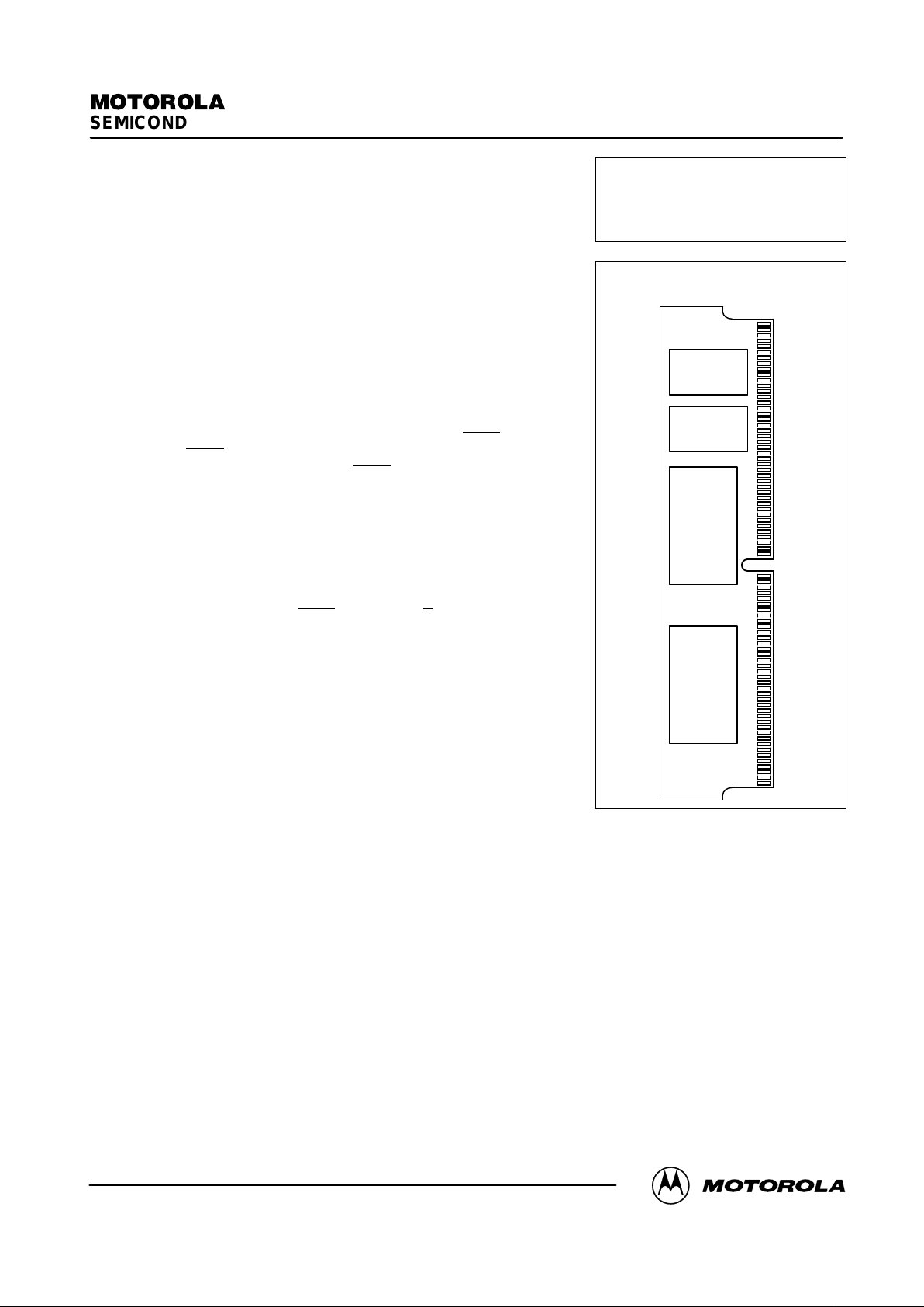
MCM64PD32
MCM64PD64
160–LEAD CARD EDGE
CASE TBD, TOP VIEW
80
43
42
1
6/14/96
Motorola, Inc. 1996
Page 2
MCM64PD32•MCM64PD64
2
MOTOROLA FAST SRAM
MCM64PD32 BLOCK DIAGRAM
BWE
CADV
ADSP
CADS
CLK0
CG
SE1
32K x 32
ADV
K
G
SW
SE2
LBO
ADSP
ADSC
DQ0 – DQ31
ZZ
V
DD
CCS
V
DD
SA0 – SA14
TIO0 – TIO7
TWE
15
13
A3 – A17
GWE
SGW
CWE0 – CWE3
SBa – SBd
SE3
ECS2
ECS1
DQ0 – DQ31
SE1
32K x 32
ADV
K
G
SW
SE2
LBO
ADSP
ADSC
DQ0 – DQ31
ZZ
SA0 – SA14
15
SGW
SBa – SBd
SE3
DQ32 – DQ63
CWE4 – CWE7
A0 – A12
DQ0 – DQ7
A13
W
A14
G
32K x 8
E
TIO8
TIO9
TIO10
VDD3
8.2 k
Ω
8.2 k
Ω
BOSEL
8.2 k
Ω
4.7 k
Ω
Page 3
MCM64PD32•MCM64PD64
3
MOTOROLA FAST SRAM
MCM64PD64 BLOCK DIAGRAM
BWE
CADV
ADSP
CADS
CLK0
CG
SE1
32K x 32
ADV
K
G
SW
SE2
LBO
ADSP
ADSC
DQ0 – DQ31
ZZ
V
DD
V
DD
SA0 – SA14
TIO0 – TIO7
TWE
13
A3 – A17
GWE
SGW
CWE0 –
CWE3
SBa – SBd
SE3
DQ0 –
DQ31
SE1
32K x 32
ADV
K
G
SW
SE2
LBO
ADSP
ADSC
DQ0 – DQ31
ZZ
SA0 – SA14
15
SGW
SBa – SBd
SE3
DQ32 –
DQ63
CWE4 –
CWE7
A0 – A12
DQ0 – DQ7
A13
W
A14
G
32K x 8
E
TIO8
TIO9
TIO10
VDD3
8.2 k
Ω
4.7 k
Ω
BOSEL
8.2 k
Ω
A18
SE1
32K x 32
ADV
K
G
SW
SE2
LBO
ADSP
ADSC
DQ0 – DQ31
ZZ
SA0 – SA14
15
SGW
SBa – SBd
SE3
SE1
32K x 32
ADV
K
G
SW
SE2
LBO
ADSP
ADSC
DQ0 – DQ31
ZZ
SA0 – SA14
SGW
SBa – SBd
SE3
V
DD
8.2 k
Ω
CCS
CLK1
Page 4
MCM64PD32•MCM64PD64
4
MOTOROLA FAST SRAM
PIN ASSIGNMENT 160–LEAD CARD EDGE MODULE (DIMM)
Pin Name Pin Name Pin Name Pin Name Pin Name
1 V
SS
33 PD1 65 DQ22 97 NC 129 DQ47
2 TIO0 34 PD3 66 DQ20 98 NC 130 DQ45
3 TIO2 35 V
SS
67 DQ18 99 V
SS
131 DQ43
4 TIO6 36 CLK1 68 VDD3 100 RSVD 132 VDD5
5 TIO4 37 V
SS
69 DQ16 101 A4 133 DQ41
6 TIO8 38 DQ62 70 DQ14 102 A6 134 DQ39
7 VDD3 39 VDD3 71 DQ12 103 A8 135 DQ37
8 TWE 40 DQ60 72 V
SS
104 A10 136 V
SS
9 CADS 41 DQ58 73 DQ10 105 VDD5 137 DQ35
10 V
SS
42 DQ56 74 DQ8 106 A17 138 DQ33
11 CWE4 43 V
SS
75 DQ6 107 V
SS
139 DQ31
12 CWE6 44 DQ54 76 VDD3 108 A9 140 VDD5
13 CWE0 45 DQ52 77 DQ4 109 A14 141 DQ29
14 CWE2 46 DQ50 78 DQ2 110 A15 142 DQ27
15 VDD3 47 DQ48 79 DQ0 111 RSVD 143 DQ25
16 CCS 48 V
SS
80 V
SS
112 PD0 144 V
SS
17 GWE 49 DQ46 81 V
SS
113 PD2 145 DQ23
18 BWE 50 DQ44 82 TIO1 114 BOSEL 146 DQ21
19 V
SS
51 DQ42 83 TIO7 115 V
SS
147 DQ19
20 A3 52 VDD3 84 TIO5 116 CLK0 148 VDD5
21 A7 53 DQ40 85 TIO3 117 V
SS
149 DQ17
22 A5 54 DQ38 86 TIO9 118 DQ63 150 DQ15
23 A11 55 DQ36 87 VDD5 119 VDD5 151 DQ13
24 A16 56 V
SS
88 TIO10 120 DQ61 152 V
SS
25 VDD3 57 DQ34 89 CADV 121 DQ59 153 DQ11
26 A18 58 DQ32 90 V
SS
122 DQ57 154 DQ9
27 V
SS
59 DQ30 91 CG 123 V
SS
155 DQ7
28 A12 60 VDD3 92 CWE5 124 DQ55 156 VDD5
29 A13 61 DQ28 93 CWE7 125 DQ53 157 DQ5
30 ADSP 62 DQ26 94 CWE1 126 DQ51 158 DQ3
31 ECS1 63 DQ24 95 VDD5 127 DQ49 159 DQ1
32 ECS2 64 V
SS
96 CWE3 128 V
SS
160 V
SS
TOP VIEW – CASE TBD
1
42
43
80
81
122
123
160
PRESENCE DETECT TABLE
Cache Size and
Functionality
PD0 PD1 PD2 PD3
256K Pipe Burst NC NC V
SS
NC
512K Pipe Burst V
SS
V
SS
NC V
SS
Page 5
MCM64PD32•MCM64PD64
5
MOTOROLA FAST SRAM
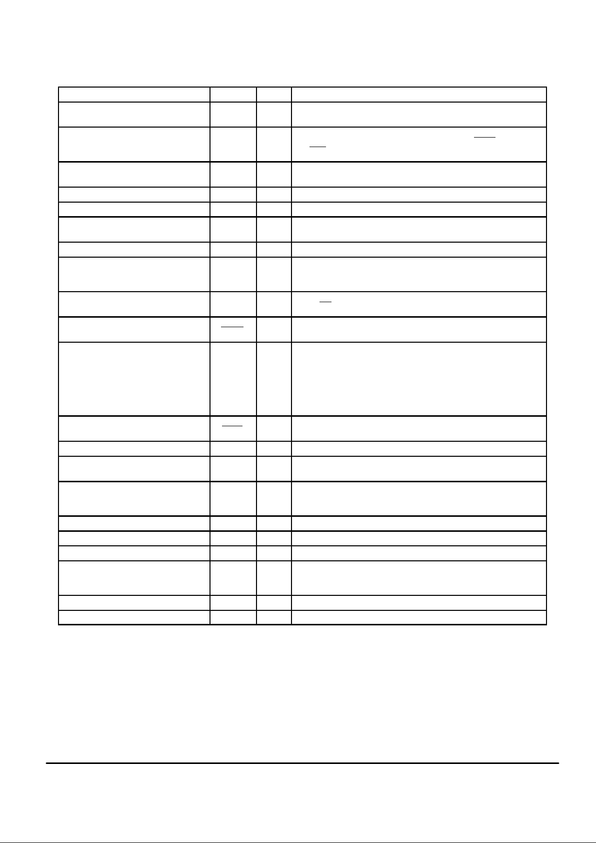
PIN DESCRIPTIONS
160–Lead Card Edge Pin Locations Symbol
Type Description
20, 21, 22, 23, 24, 26, 28, 29,
101, 102, 103, 104, 106, 108, 109, 110
A3 – A18 Input Address Inputs: These inputs are registered into data RAMs and must
meet setup and hold times. The tag RAM addresses are not registered.
30 ADSP Input Address Status Processor: Initiates READ, WRITE, or chip deselect
cycle (Exception–chip deselect dGs not occur when ADSP
is asserted
and CCS
is high.
114 BOSEL Input Burst Order Select: NC for interleaved burst counter. T ie to ground for
linear burst counter.
18 BWE Input Byte Write Enable: To be used in future modules.
9 CADS Input Cache Address Status: Initiates READ, WRITE, or chip deselect cycle.
89 CADV Input Cache Burst Advance: Increments address count in accordance with
interleaved count style.
16 CCS Input Chip Select: Active low chip enable for data RAMs.
91 CG Input Cache Output Enable: Active low asynchronous input.
Low – enables output buffers (DQ pins)
High – DQx pins are high impedance.
36, 116 CLK0,
CLK1
Input Clock: This signal registers the address, data in, and all control signals
except CG
.
11, 12, 13, 14, 92, 93, 94, 96 CWE0 –
CWE7
Input Cache Data Byte Write Enable: Active low write signal for data RAMs.
38, 40, 41, 42, 44, 45, 46, 47, 49, 50, 51,
53, 54, 55, 57, 58, 59, 61, 62, 63, 65, 66,
67, 69, 70, 71, 73, 74, 75, 77, 78, 79,
118, 120, 121, 122, 124, 125, 126, 127,
129, 130, 131, 133, 134, 135, 137, 138,
139, 141, 142, 143, 145, 146, 147, 149,
150, 151, 153, 154, 155, 157, 158, 159
DQ0 –
DQ63
I/O Synchronous Data I/O:
Drives data out of data RAMs during READ cycles.
Stores data to data RAMs during WRITE cycles.
31, 32 ECS1,
ECS2
Input Expansion Chip Select
17 GWE Input Global Write Enable: To be used in future modules.
33, 34, 112, 113 PD0 –
PD3
— Presence Detect: See Presence Detect Table
2, 3, 4, 5, 6, 82, 83, 84, 85, 86, 88 TIO0 –
TIO10
I/O Tag RAM I/O:
Drives data out during tag compare cycles.
Stores data to tag RAM during tag WRITE cycles.
8 TWE Input Tag Write Enable: Active low write signal for tag RAMs.
7, 15, 25, 39, 52, 60, 68, 76 VDD3 Supply Power Supply: 3.3 V + 10%, – 5%.
87, 95, 105, 119, 132, 140, 148, 156 VDD5 Supply Power Supply: 5.0 V ± 5%.
1, 10, 19, 27, 35, 37, 43, 48, 56, 64, 72,
80, 81, 90, 99, 107, 115, 117, 123, 128,
136, 144, 152, 160
V
SS
Supply Ground.
100, 111 RSVD — No Connection: Reserved for future use.
97, 98 NC — No Connection: There is no connection to the module.
Page 6

MCM64PD32•MCM64PD64
6
MOTOROLA FAST SRAM
SYNCHRONOUS TRUTH TABLE (See Notes 1, 2, and 3)
CCS
ADSP CADS CADV CWEx CLK0 Address Used Operation
H X L X X L–H N/A Deselected
L L X X X L–H External Address Read Cycle, Begin Burst
L H L X L L–H External Address Write Cycle, Begin Burst
L H L X H L–H External Address Read Cycle, Begin Burst
X H H L L L–H Next Address Write Cycle, Continue Burst
X H H L H L–H Next Address Read Cycle, Continue Burst
X H H H L L–H Current Address Write Cycle, Suspend Burst
X H H H H L–H Current Address Read Cycle, Suspend Burst
H X H L L L–H Next Address Write Cycle, Continue Burst
H X H L H L–H Next Address Read Cycle, Continue Burst
H X H H L L–H Current Address Write Cycle, Suspend Burst
H X H H H L–H Current Address Read Cycle, Suspend Burst
NOTES:
1. X means Don’t Care.
2. All inputs except CG
must meet setup and hold times for the low–to–high transition of clock (CLK0/1).
3. Wait states are inserted by suspending burst.
ASYNCHRONOUS TRUTH TABLE (See Notes 1 and 2)
Operation
CG I/O Status
Read L Data Out
Read H High–Z
Write X High–Z — Data In
Deselected X High–Z
NOTES:
1. X means Don’t Care.
2. For a write operation following a read operation, G
must be high before the input data
required setup time and held high through the input data hold time.
DC ABSOLUTE MAXIMUM RATINGS (Voltages Referenced to V
SS
= 0 V)
Rating
Symbol Value Unit
Power Supply Voltage VDD3 – 0.5 to + 4.6 V
Voltage Relative to V
SS
Vin, V
outVSS
– 0.5 to VDD3 + 0.5 V
Output Current (per I/O) I
out
± 20 mA
Temperature Under Bias T
bias
– 10 to + 85 °C
Operating Temperature T
A
0 to +70 °C
Storage Temperature T
stg
– 65 to + 150 °C
NOTE: Permanent device damage may occur if ABSOLUTE MAXIMUM RATINGS are
exceeded. Functional operation should be restricted to RECOMMENDED OPERATING CONDITIONS. Exposure to higher than recommended voltages for
extended periods of time could affect device reliability.
This device contains circuitry to protect the
inputs against damage due to high static voltages or electric fields; however, it is advised
that normal precautions be taken to avoid
application of any voltage higher than maximum rated voltages to this high–impedance
circuit.
This BiCMOS memory circuit has been
designed to meet the dc and ac specifications
shown in the tables, after thermal equilibrium
has been established.
This device contains circuitry that will
ensure the output devices are in High–Z at
power up.
Page 7

MCM64PD32•MCM64PD64
7
MOTOROLA FAST SRAM
DC OPERA TING CONDITIONS AND CHARACTERISTICS
(VDD = 3.3 V + 10%, – 5%, TJ = 20 to + 110 °C, Unless Otherwise Noted)
RECOMMENDED OPERATING CONDITIONS
(Voltages referenced to VSS = 0 V)
Parameter
Symbol Min Max Unit Notes
Supply Voltage (Operating Voltage Range) V
DD
3.135 3.6 V 1
Input High Voltage V
IH
2.0 VDD + 0.3 V 2
Input Low Voltage V
IL
– 0.5 0.8 V 3
NOTES:
1. JEDEC specification 8–1A specifies ± 0.3 V tolerance for VDD.
2. VIH (max) = VDD + 0.3 V dc; VIH (max) = VDD + 2.0 V ac (pulse width ≤ 20 ns) for I ≤ 20.0 mA.
3. VIL (min) = – 0.5 V dc; VIL (min) = – 2.0 V ac (pulse width ≤ 20 ns) for I ≤ 20.0 mA.
DC CHARACTERISTICS
Parameter Symbol Min Max Unit Notes
Input Leakage Current (All Inputs, Vin = 0 to VDD3) I
lkg(I)
— ± 1.0 µA
Output Leakage Current (CG = VIH) I
lkg(O)
— ± 1.0 µA
TTL Output Low Voltage (IOL = + 8.0 mA) V
OL
— 0.4 V 1
TTL Output High Voltage (IOH = – 4.0 mA) V
OH
2.4 — V 1
NOTES:
1. Champing diodes exist to VSS and VDD.
POWER SUPPLY CURRENTS
Parameter Symbol Max Unit
AC Supply Current (CG = VIH, CCS = VIL, I
out
= 0 mA, All Inputs = VIL or VIH, MCM64PD32
VIL = 0.0 V and VIH ≥ 3.0 V, Cycle Time ≥ t
KHKH
min) MCM64PD64
I
DDA
720
880
mA
AC Standby Current (CG = VIH, CCS = VIL, I
out
= 0 mA, All Inputs = VIL or VIH, MCM64PD32
VIL = 0.0 V and VIH ≥ 3.0 V, Cycle Time ≥ t
KHKH
min) MCM64PD64
I
SB1
200
490
mA
CAPACITANCE (f = 1.0 MHz, dV = 3.0 V, T
J
= 20 to 110°C, Periodically Sampled Rather Than 100% Tested)
Parameter
Symbol Max Unit
Input Capacitance MCM64PD32
MCM64PD64
C
in
22
32
pF
Input/Output Capacitance (DQ0 – DQ63) MCM64PD32
MCM64PD64
C
I/O
8
16
pF
Page 8

MCM64PD32•MCM64PD64
8
MOTOROLA FAST SRAM
DATA RAMs AC OPERATING CONDITIONS AND CHARACTERISTICS
(VDD = 3.3 V + 10%, – 5% TJ = 20 to + 110 °C, Unless Otherwise Noted)
Input Timing Measurement Reference Level 1.5 V. . . . . . . . . . . . . . .
Input Pulse Levels 0 to 3.0 V. . . . . . . . . . . . . . . . . . . . . . . . . . . . . . . . .
Input Rise/Fall Time 2 ns. . . . . . . . . . . . . . . . . . . . . . . . . . . . . . . . . . . .
Output Timing Reference Level 1.5 V. . . . . . . . . . . . . . . . . . . . . . . . . .
Output Load See Figure 3 Unless Otherwise Noted. . . . . . . . . . . . . .
2.4
INPUT
WA VEFORM
t
r
TEST POINT
(UNLOADED OUTPUT)
OUTPUT
BUFFER
2.4
0.4 0.4
OUTPUT
WA VEFORM
OUTPUT LOAD
t
f
UNLOADED RISE AND FALL TIME MEASUREMENT
NOTES:
1. Input waveform has a slew rate of 1 V/ns.
2. Rise time is measured from 0.4 V to 2.4 V unloaded.
3. Fall time is measured from 2.4 V to 0.4 V unloaded.
Figure 1. Unloaded Rise and Fall Time Characterization
Page 9

MCM64PD32•MCM64PD64
9
MOTOROLA FAST SRAM
DATA RAMs READ/WRITE CYCLE TIMING (See Notes 1, 2, and 3)
MCM64PD32–66
Parameter Symbol Min Max Unit Notes
Cycle Time t
KHKH
15 — ns
Clock Access Time t
KHQV
— 8 ns 5
Output Enable to Output Valid t
GLQV
— 6 ns 5
Clock High to Output Active t
KHQX1
0 — ns 5, 7
Clock High to Output Change t
KHQX2
2 — ns 5, 7
Output Enable to Output Active t
GLQX
0 — ns 5, 7
Output Disable to Q High–Z t
GHQZ
— 8 ns 6, 7
Clock High to Q High–Z t
KHQZ
2 8 ns 6, 7
Clock High Pulse Width t
KHKL
5 — ns
Clock Low Pulse Width t
KLKH
5 — ns
Setup Times: Address
Address Status
Data In
Write
Address Advance
Chip Enable
t
AVKH
t
ADSVKH
t
DVKH
t
WVKH
t
ADVVKH
t
EVKH
2.5 — ns 4
Hold Times: Address
Address Status
Data In
Write
Address Advance
Chip Enable
t
KHAX
t
KHADSX
t
KHDX
t
KHWX
t
KHADVX
t
KHEX
0.5 — ns 4
NOTES:
1. Write applies to all SBx
, SW, and SGW signals when the chip is selected and ADSP high.
2. Chip Enable applies to all SE1
, SE2 and SE3 signals whenever ADSP or ADSC is asserted.
3. All read and write cycle timings are referenced from K or G
.
4. G
is a don’t care after write cycle begins. To prevent bus contention, G should be negated prior to start of write cycle.
5. Tested per AC Test Load.
6. Measured at
± 200 mV from steady state. Tested per High–Z Test Load.
7. This parameter is sampled and is not 100% tested.
Page 10

MCM64PD32•MCM64PD64
10
MOTOROLA FAST SRAM
TEST POINT
3.6
3.135
2.8
1.65
1.4
0
0 – 40 –120
TEST POINT
V
DD
1.65
1.8
0.3
0
0 46 120
CURRENT (mA)
CURRENT (mA)
VOLTAGE (V)VOLTAGE (V)
VOLTAGE (V)
PULL–UP
I (mA) Min I (mA) Max
– 0.5
0
1.4
1.65
2
3.135
3.6
– 40
– 40
– 40
– 37
–28
0
0
– 120
– 120
– 120
– 104
– 81
– 20
0
VOLTAGE (V)
PULL–DOWN
I (mA) Min I (mA) Max
– 0.5
0
0.5
1
1.65
1.8
3.6
4
– 34
0
17
35
45
46
46
46
– 126
0
47
90
114
120
120
120
(a) Pull–Up
(b) Pull–Down
–5
5
80
DC DRIVE
POINT
AC DRIVE
POINT
AC DRIVE
POINT
DC DRIVE
POINT
– 80
NOTES:
1. Driver impedance @ 1.65 V = 15.9 to 44.6 Ω.
2. Meets the temperature and voltage range specified in DC Characteristics tables.
3. This drawing is not to scale. Comparisons should be made to the table in Figure 2a.
NOTES:
1. Driver impedance @ 1.65 V = 15.9 to 44.6 Ω.
2. Meets the temperature and voltage range specified in DC Characteristics tables.
3. This drawing is not to scale. Comparisons should be made to the table in Figure 2b.
Figure 2. Output Buffer Characteristics
Page 11

MCM64PD32•MCM64PD64
11
MOTOROLA FAST SRAM
BURST READSINGLE READ
CADS
t
KHKL
t
KHKH
DQx
ESC1
CLK0, CLK1
ADSP
CADV
Q(A)
BURST WRITE
ADSP , Ax
Ax
AB
DATA RAMs READ/WRITE CYCLES
t
KLKH
CD
CCS
W
Q(B) Q(B+1)
t
KHQV
BURST WRAPS AROUND
Q(B+2) Q(B+3)
Q(B) D(C) D(C+1) D(C+2) D(C+3) Q(D)
t
KHQV
DESELECTED SINGLE READ
ESC1 IGNORED
CG
t
KHQX1
t
KHQX2
t
GHQZ
t
GLQX
Q(n–1)
t
KHQZ
(ADDRESS)
Note: W low = GWE low and/or BWE and CWEx low.
Page 12

MCM64PD32•MCM64PD64
12
MOTOROLA FAST SRAM
T AG RAM AC OPERATING CONDITIONS AND CHARACTERISTICS
(VDD = 3.3 V ± 0.3 V, TJ = 20 to + 110°C, Unless Otherwise Noted)
Input Timing Measurement Reference Level 1.5 V. . . . . . . . . . . . . . .
Input Pulse Levels 0 to 3.0 V. . . . . . . . . . . . . . . . . . . . . . . . . . . . . . . . .
Input Rise/Fall Time 3 ns. . . . . . . . . . . . . . . . . . . . . . . . . . . . . . . . . . . .
Output Timing Measurement Reference Level 1.5 V. . . . . . . . . . . . .
Output Load Figure 3a Unless Otherwise Noted. . . . . . . . . . . . . . . . .
TAG RAM READ CYCLE (See Note 1 and 5)
–15
Parameter Symbol Min Max Unit Notes
Read Cycle Time t
AVAV
15 — ns 2
Address Access Time t
AVQV
— 15 ns
Output Hold from Address Change t
AXQX
4 — ns 3, 4
NOTES:
1. CWE
is high for read cycle.
2. All timings are referenced from the last valid address to the first address transition.
3. Transition is measured ±500 mV from steady–state voltage with load of Figure 3b.
4. This parameter is sampled and not 100% tested.
5. Device is continuously selected (CG
= VIL).
TAG RAM READ CYCLE (See Note 5)
Q (DATA OUT)
Ax (ADDRESS)
DATA VALIDPREVIOUS DATA VALID
t
AVAV
t
AXQX
t
AVQV
OUTPUT
Z0 = 50
Ω
50
Ω
VL = 1.5 V
(a) (b)
5 pF
+3.3 V
OUTPUT
351
Ω
317
Ω
TIMING LIMITS
The table of timing values shows either a
minimum or a maximum limit for each parameter. Input requirements are specified from
the external system point of view. Thus, address setup time is shown as a minimum
since the system must supply at least that
much time (even though most devices do not
require it). On the other hand, responses from
the memory are specified from the device
point of view. Thus, the access time is shown
as a maximum since the device never provides data later than that time.
Figure 3. AC Test Loads
Page 13

MCM64PD32•MCM64PD64
13
MOTOROLA FAST SRAM
TAG RAM WRITE CYCLE (See Notes 1 and 2)
–15
Parameter Symbol Min Max Unit Notes
Write Cycle Time t
AVAV
15 — ns 3
Address Setup Time t
AVWL
0 — ns
Address Valid to End of W rite t
AVWH
12 — ns
Data Valid to End of W rite t
DVWH
7 — ns
Data Hold Time t
WHDX
0 — ns
Write Low to Output High–Z t
WLQZ
0 7 ns 5,6,7
Write High to Output Active t
WHQX
4 — ns 5,6,7
Write Recovery Time t
WHAX
0 — ns
NOTES:
1. A write occurs when CWE
is low.
2. If CG
goes low coincident with or after CWE goes low, the output will remain in a high impedance state.
3. All timings are referenced from the last valid address to the first address transition.
4. If CG
≥ VIH, the output will remain in a high impedance state.
5. At any given voltage and temperature, t
WLQZ
(max) is less than t
WHQX
(min), both for a given device and from device to device.
6. Transition is measured ±500 mV from steady–state voltage with load of Figure 3B.
7. This parameter is sampled and not 100% tested.
TAG RAM WRITE CYCLE (See Notes 1 and 2)
DATA VALID
t
DVWH
t
AVWL
t
AVWH
t
AVAV
t
WHAX
t
WLWH
t
WHDX
t
WLQZ
t
WHQX
HIGH Z
HIGH Z
AX (ADDRESS)
TWE
Q (DATA OUT)
D (DATA IN)
Page 14

MCM64PD32•MCM64PD64
14
MOTOROLA FAST SRAM
ORDERING INFORMATION
(Order by Full Part Number)
64PD32
MCM 64PD64 XX XX
Motorola Memory Prefix
Part Number
Full Part Number —MCM64PD32SG66 MCM64PD64SG66
Speed (66 = 66 MHz)
Package (SG = Gold Pad SIMM)
Page 15

MCM64PD32•MCM64PD64
15
MOTOROLA FAST SRAM
P ACKAGE DIMENSIONS
160–LEAD
CARD EDGE MODULE
CASE TBD
M
P
(N)
A
SIDE VIEW
E
L
K
R
160X
H160X
R
W
D
160X
156X
Y
L
0.004 (0.1) X
S
T
DIM MIN MAX MIN MAX
MILLIMETERSINCHES
A 4.330 4.350 109.98 110.49
B 1.120 1.140 28.45 28.96
C ––– 0.454 ––– 11.53
D 0.033 0.037 0.84 0.94
E 2.265 2.275 57.53 57.79
F 0.075 BSC 1.91 BSC
G 0.050 BSC 1.27 BSC
H ––– 0.030 ––– 0.51
J 0.055 0.069 1.40 1.75
K 0.210 ––– 5.33 –––
L 1.955 1.965 49.66 49.91
M 2.155 2.165 54.74 54.99
N 0.110 REF 2.79 REF
P 0.300 ––– 7.62 –––
R 0.492 0.512 7.24 7.75
V 0.300 ––– 7.62 –––
W 0.040 0.060 1.02 1.52
AB ––– 0.262 ––– 6.66
AC 0.072 0.076 1.83 1.93
NOTES:
1. DIMENSIONING AND TOLERANCING PER ANSI
Y14.5M, 1982.
2. CONTROLLING DIMENSION: INCH.
3. CARD THICKNESS APPLIES ACROSS TABS AND
INCLUDES PLATING AND/OR METALLIZATION.
4. DIMENSIONS C AND V DEFINE A
DOUBLE–SIDED MODULE.
5. DIMENSION AB DEFINES OPTIONAL
SINGLE–SIDED MODULE.
6. STRAIGHTNESS CALLOUT APPLIES TO TAB
AREA ONLY.
G
2X
BACK VIEW
COMPONENT
VIEW AA
AC
F
–X–
–Y–
B
VIEW
AA
MIN .285 inches,
COMPONENT
80 43 42 1
AREA
FRONT VIEW
V
NOTE 4
AB
NOTE 5
J NOTE 6
M
0.012 (0.3)
–T–
AREA
160 123 122 81
C
NOTE 4
NOTE: Case Outline number to be determined.
MAX .305 inches
Page 16

MCM64PD32•MCM64PD64
16
MOTOROLA FAST SRAM
Motorola reserves the right to make changes without further notice to any products herein. Motorola makes no warranty , representation or guarantee regarding
the suitability of its products for any particular purpose, nor does Motorola assume any liability arising out of the application or use of any product or circuit, and
specifically disclaims any and all liability, including without limitation consequential or incidental damages. “T ypical” parameters which may be provided in Motorola
data sheets and/or specifications can and do vary in different applications and actual performance may vary over time. All operating parameters, including “Typicals”
must be validated for each customer application by customer’s technical experts. Motorola does not convey any license under its patent rights nor the rights of
others. Motorola products are not designed, intended, or authorized for use as components in systems intended for surgical implant into the body, or other
applications intended to support or sustain life, or for any other application in which the failure of the Motorola product could create a situation where personal injury
or death may occur. Should Buyer purchase or use Motorola products for any such unintended or unauthorized application, Buyer shall indemnify and hold Motorola
and its officers, employees, subsidiaries, affiliates, and distributors harmless against all claims, costs, damages, and expenses, and reasonable attorney fees
arising out of, directly or indirectly, any claim of personal injury or death associated with such unintended or unauthorized use, even if such claim alleges that
Motorola was negligent regarding the design or manufacture of the part. Motorola and are registered trademarks of Motorola, Inc. Motorola, Inc. is an Equal
Opportunity/Affirmative Action Employer.
How to reach us:
USA/EUROPE /Locations Not Listed: Motorola Literature Distribution; JAPAN: Nippon Motorola Ltd.; Tatsumi–SPD–JLDC, 6F Seibu–Butsuryu–Center,
P.O. Box 20912; Phoenix, Arizona 85036. 1–800–441–2447 or 602–303–5454 3–14–2 Tatsumi Koto–Ku, Tokyo 135, Japan. 03–81–3521–8315
MFAX: RMF AX0@email.sps.mot.com – TOUCHT ONE 602–244–6609 ASIA/PACIFIC: Motorola Semiconductors H.K. Ltd.; 8B Tai Ping Industrial Park,
INTERNET: http://Design–NET.com 51 Ting Ko k Road, Tai Po, N.T., Hong Kong. 852–26629298
MCM64PD32/D
*MCM64PD32/D*
◊
 Loading...