

Page 1
MCM63P736•MCM63P818
1
MOTOROLA FAST SRAM
Product Preview
128K x 36 and 256K x 18 Bit
Pipelined BurstRAM
Synchronous Fast Static RAM
The MCM63P736 and MCM63P818 are 4M bit synchronous fast static RAMs
designed to provide a burstable, high performance, secondary cache for the
PowerPC and other high performance microprocessors. The MCM63P736 is
organized as 128K words of 36 bits each and the MCM63P818 is organized as
256K words of 18 bits each. These devices integrate input registers, an output
register, a 2–bit address counter , and high speed SRAM onto a single monolithic
circuit for reduced parts count in cache data RAM applications. Synchronous design allows precise cycle control with the use of an external clock (K).
Addresses (SA), data inputs (DQx), and all control signals except output
enable (G
), sleep mode (ZZ), and linear burst order (LBO) are clock (K) controlled
through positive–edge–triggered noninverting registers.
Bursts can be initiated with either ADSP
or ADSC input pins. Subsequent burst
addresses can be generated internally by the MCM63P736 and MCM63P818
(burst sequence operates in linear or interleaved mode dependent upon the state
of LBO
) and controlled by the burst address advance (ADV) input pin.
Write cycles are internally self–timed and are initiated by the rising edge of the
clock (K) input. This feature eliminates complex off–chip write pulse generation
and provides increased timing flexibility for incoming signals.
Synchronous byte write (SBx
), synchronous global write (SGW), and synchro-
nous write enable (SW
) are provided to allow writes to either individual bytes or
to all bytes. The bytes are designated as “a”, “b”, etc. SBa
controls DQa, SBb con-
trols DQb, etc. Individual bytes are written if the selected byte writes SBx
are asserted with SW. All bytes are written if either SGW is asserted or if all SBx and
SW
are asserted.
For read cycles, pipelined SRAMs output data is temporarily stored by an
edge–triggered output register and then released to the output buffers at the next
rising edge of clock (K).
The MCM63P736 and MCM63P818 operate from a 3.3 V core power supply
and all outputs operate on a 2.5 V or 3.3 V power supply. All inputs and outputs
are JEDEC standard JESD8–5 compatible.
• MCM63P736/MCM63P818–133 = 4 ns Access/7.5 ns Cycle (133 MHz)
MCM63P736/MCM63P818–100 = 5 ns Access/10 ns Cycle (100 MHz)
MCM63P736/MCM63P818–66 = 7 ns Access/15 ns Cycle (66 MHz)
• 3.3 V + 10%, – 5% Core Power Supply, 2.5 V or 3.3 V I/O Supply
• ADSP
, ADSC, and ADV Burst Control Pins
• Selectable Burst Sequencing Order (Linear/Interleaved)
• Two–Cycle Deselect Timing
• Internally Self–Timed Write Cycle
• Byte Write and Global Write Control
• Sleep Mode (ZZ)
• PB1 Version 2.0 Compatible
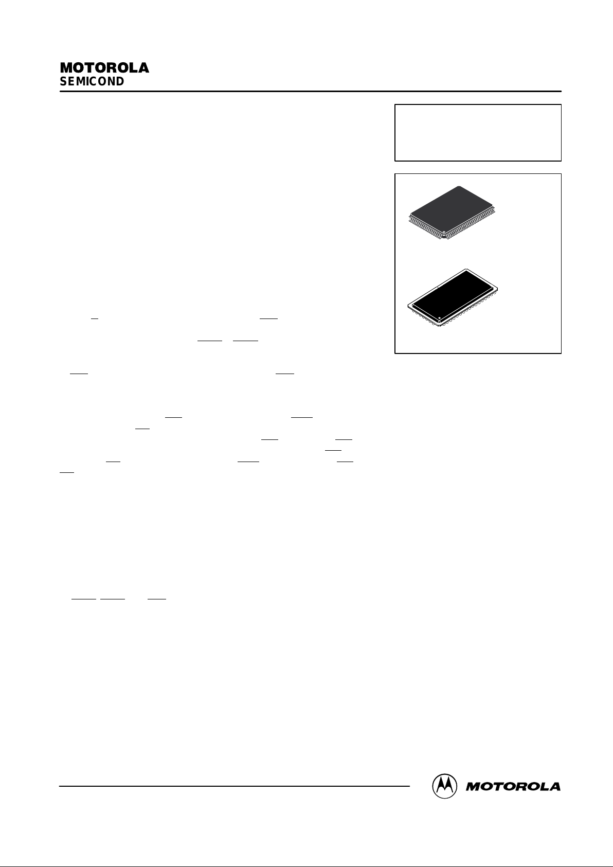
• JEDEC Standard 119–Pin PBGA and 100–Pin TQFP Packages
The PowerPC name is a trademark of IBM Corp., used under license therefrom.
This document contains information on a product under development. Motorola reserves the right to change or discontinue this product without notice.
Order this document
by MCM63P736/D
MOTOROLA
SEMICONDUCTOR TECHNICAL DATA
MCM63P736
MCM63P818
ZP PACKAGE
PBGA
CASE 999–01
TQ PACKAGE
TQFP
CASE 983A–01
10/8/97
Motorola, Inc. 1997
Page 2
MCM63P736•MCM63P818
2
MOTOROLA FAST SRAM
WRITE
REGISTER
a
WRITE
REGISTER
b
ENABLE
REGISTER
BURST
COUNTER
ADSP
G
CLR
WRITE
REGISTER
c*
WRITE
REGISTER
d*
SBa
SBb
SBc*
SBd*
SE3
15/16
17/18
SGW
DATA–OUT
REGISTER
ENABLE
REGISTER
K2 K
ADDRESS
REGISTER
17/18
DATA–IN
REGISTER
128K x 36 /
256K x 18
ARRAY
SE2
LBO
ADV
K
ADSC
SA
SA1
SA0
SW
SE1
K
4/2
36/18
2
2
K2
DQa – DQd /
DQa – DQb
36/18
FUNCTIONAL BLOCK DIAGRAM
WRITE
REGISTER
K
ZZ
*Valid only for MCM63P736.
Page 3
MCM63P736•MCM63P818
3
MOTOROLA FAST SRAM
6543217
B
C
V
SS
G
A
D
E
F
H
J
V
SS
V
SS
SBb
V
SS
SA
V
SS
V
SS
V
SS
SA SA SA SA
SA SA SA SA
NC SA SA NC
NC
NC
DQb
SA SA
NC
ZZ
SW
DQa
DQa
V
DDQ
V
DDQ
DQb
V
DDQ
DQb
DQb
DQa
DQa
NCV
DD
NC
SA
NCNC
NC
NC
DQd DQd VSSSA0
NC
LBO
DQa
DQaSA1V
SS
DQdDQd
V
DDQ
DQd V
SS
NC
DQa
DQaSBa
SBdDQdDQd
DQd DQd V
SS
KV
SS
DQc
DQa
V
DD
NCV
DD
NCV
DD
V
DDQ
DQc VSSSGW
DQb
DQb
DQbADV
SBcDQcDQc
V
DDQ
DQc V
SS
G
DQbSE1V
SS
DQcDQc
DQc DQc VSSNC DQb
V
DD
NC
NC SE2 SA ADSC
ADSP
K
L
M
N
P
R
T
U
V
DDQ
V
DDQ
SE3
V
DDQ
V
DDQ
NC
71
72
DQc
V
DDQ
DQb
69
70
66
67
68
64
65
61
62
63
3738343536 42433940 41 454644
60
59
58
57
56
55
54
53
52
51
31 3233
74
75
76
77
78
79
80
50494847
DQb
DQb
V
SS
DQb
DQb
DQb
DQb
V
SS
V
DDQ
DQb
DQb
V
DDQ
V
SS
V
SS
V
DDQ
DQc
DQc
DQc
DQc
DQc
DQc
DQc
NC
SASASE1
SBd
K
SBc
ADV
G
SA0
SASASA
SA
NC
NC
NC
LBO
SA1
V
DD
V
DD
NC
DQa
V
SS
DQa
DQa
DQa
DQa
V
SS
V
DDQ
DQa
DQa
V
SS
V
DDQ
DQa
DQa
DQd
V
DD
V
SS
V
SS
V
DDQ
DQd
DQd
DQd
DQd
DQd
73
DQc
94 93979695 89889291 90 86858710099 98 81828384
10
9
12
11
15
14
13
17
16
20
19
18
21
22
23
24
25
26
27
28
29
30
7
6
5
4
3
2
1
8
SA
SA
SW
SE2
SE3
VSSV
DD
ZZ
NC
V
DDQ
V
SS
DQd
DQd
DQd
SA
SA
SASASA
SA
SA
NC
V
SS
ADSP
ADSC
SGW
SBa
SBb
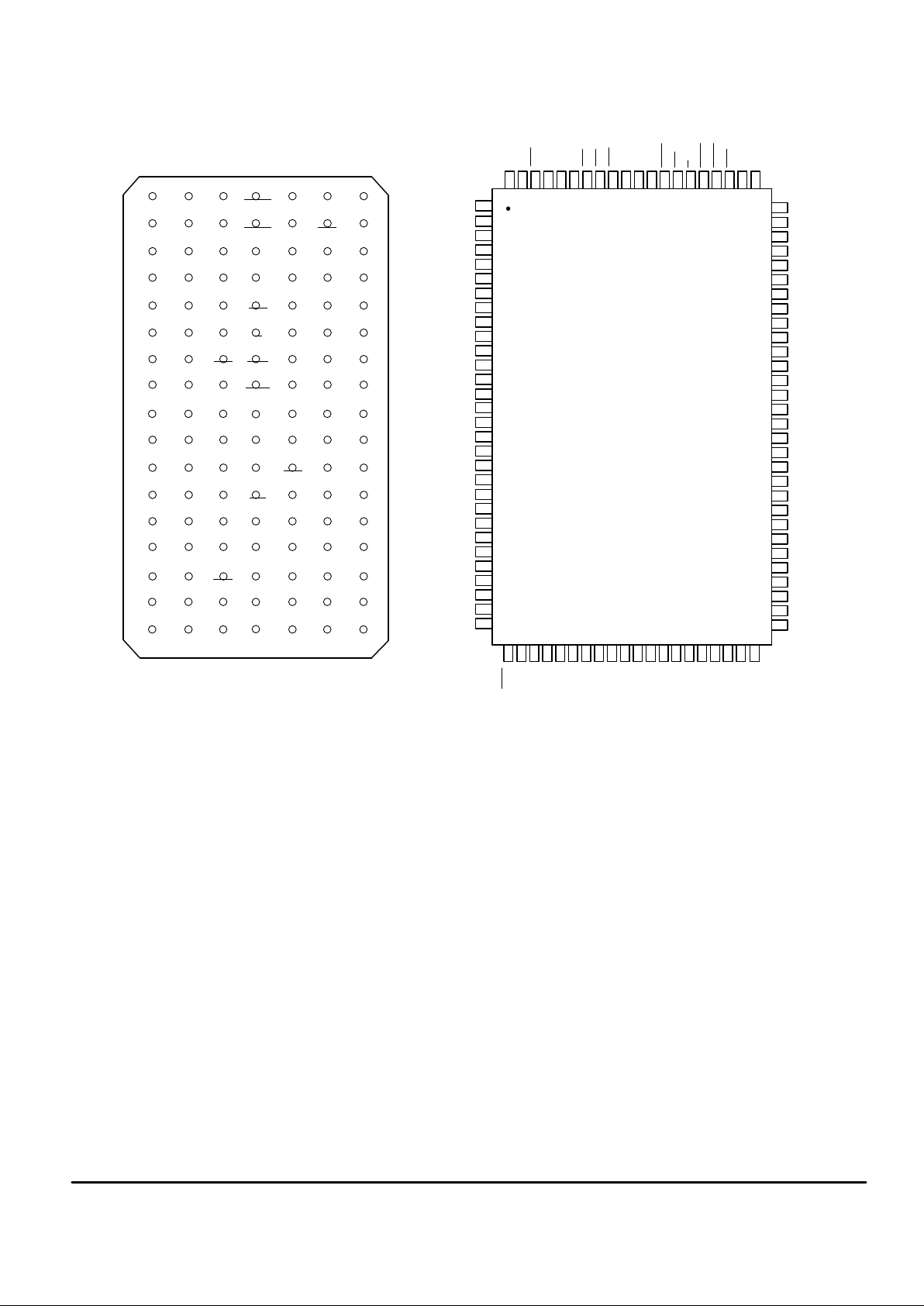
TOP VIEW 119 BUMP PBGA
Not to Scale
TOP VIEW 100 PIN TQFP
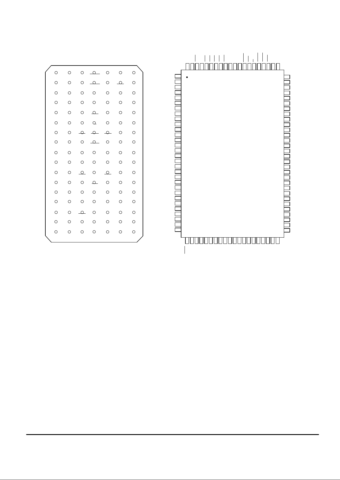
MCM63P736 PIN ASSIGNMENTS
Page 4
MCM63P736•MCM63P818
4
MOTOROLA FAST SRAM
MCM63P736 PBGA PIN DESCRIPTIONS
Pin Locations Symbol
Type Description
4B ADSC Input Synchronous Address Status Controller: Active low, interrupts any
ongoing burst and latches a new external address. Used to initiate a
READ, WRITE, or chip deselect.
4A ADSP Input Synchronous Address Status Processor: Active low, interrupts any
ongoing burst and latches a new external address. Used to initiate a
new READ or chip deselect (exception — chip deselect does not occur
when ADSP
is asserted and SE1 is high).
4G ADV Input Synchronous Address Advance: Increments address count in
accordance with counter type selected (linear/interleaved).
(a) 6K, 7K, 6L, 7L, 6M, 6N, 7N, 6P, 7P
(b) 6D, 7D, 6E, 7E, 6F, 6G, 7G, 6H, 7H
(c) 1D, 2D, 1E, 2E, 2F, 1G, 2G, 1H, 2H
(d) 1K, 2K, 1L, 2L, 2M, 1N, 2N, 1P, 2P
DQx I/O Synchronous Data I/O: “x” refers to the byte being read or written
(byte a, b, c, d).
4F G Input Asynchronous Output Enable Input:
Low — enables output buffers (DQx pins).
High — DQx pins are high impedance.
4K K Input Clock: This signal registers the address, data in, and all control signals
except G
, LBO, and ZZ.
3R LBO Input Linear Burst Order Input: This pin must remain in steady state (this
signal not registered or latched). It must be tied high or low.
Low — linear burst counter (68K/PowerPC).
High — interleaved burst counter (486/i960/Pentium).
2A, 3A, 5A, 6A, 3B, 5B, 2C, 3C,
5C, 6C, 2R, 6R, 3T, 4T, 5T
SA Input Synchronous Address Inputs: These inputs are registered and must
meet setup and hold times.
4N, 4P SA1, SA0 Input Synchronous Address Inputs: These pins must be wired to the two
LSBs of the address bus for proper burst operation. These inputs are
registered and must meet setup and hold times.
5L, 5G, 3G, 3L
(a) (b) (c) (d)
SBx Input Synchronous Byte Write Inputs: “x” refers to the byte being written (byte
a, b, c, d). SGW
overrides SBx.
4E SE1 Input Synchronous Chip Enable: Active low to enable chip.
Negated high — blocks ADSP
or deselects chip when ADSC is
asserted.
2B SE2 Input Synchronous Chip Enable: Active high for depth expansion.
6B SE3 Input Synchronous Chip Enable: Active low for depth expansion.
4H SGW Input Synchronous Global Write: This signal writes all bytes regardless of the
status of the SBx
and SW signals. If only byte write signals SBx are
being used, tie this pin high.
4M SW Input Synchronous Write: This signal writes only those bytes that have been
selected using the byte write SBx
pins. If only byte write signals SBx
are being used, tie this pin low.
7T ZZ Input Sleep Mode: This active high asynchronous signal places the RAM into
the lowest power mode. The ZZ pin disables the RAMs internal clock
when placed in this mode. When ZZ is negated, the RAM remains in
low power mode until it is commanded to READ or WRITE. Data
integrity is maintained upon returning to normal operation.
4C, 2J, 4J, 6J, 4R V
DD
Supply Core Power Supply.
1A, 7A, 1F, 7F, 1J, 7J, 1M, 7M, 1U, 7U V
DDQ
Supply I/O Power Supply.
3D, 5D, 3E, 5E, 3F, 5F, 3H, 5H,
3K, 5K, 3M, 5M, 3N, 5N, 3P, 5P
V
SS
Supply Ground.
1B, 7B, 1C, 7C, 4D, 3J, 5J, 4L, 1R, 5R,
7R, 1T, 2T, 6T, 2U, 3U, 4U, 5U, 6U
NC — No Connection: There is no connection to the chip.
Page 5
MCM63P736•MCM63P818
5
MOTOROLA FAST SRAM
MCM63P736 TQFP PIN DESCRIPTIONS
Pin Locations Symbol
Type Description
85 ADSC Input Synchronous Address Status Controller: Active low, interrupts any
ongoing burst and latches a new external address. Used to initiate a
READ, WRITE, or chip deselect.
84 ADSP Input Synchronous Address Status Processor: Active low, interrupts any
ongoing burst and latches a new external address. Used to initiate a
new READ or chip deselect (exception — chip deselect does not occur
when ADSP
is asserted and SE1 is high).
83 ADV Input Synchronous Address Advance: Increments address count in
accordance with counter type selected (linear/interleaved).
(a) 51, 52, 53, 56, 57, 58, 59, 62, 63
(b) 68, 69, 72, 73, 74, 75, 78, 79, 80
(c) 1, 2, 3, 6, 7, 8, 9, 12, 13
(d) 18, 19, 22, 23, 24, 25, 28, 29, 30
DQx I/O Synchronous Data I/O: “x” refers to the byte being read or written
(byte a, b, c, d).
86 G Input Asynchronous Output Enable Input:
Low — enables output buffers (DQx pins).
High — DQx pins are high impedance.
89 K Input Clock: This signal registers the address, data in, and all control signals
except G
, LBO, and ZZ.
31 LBO Input Linear Burst Order Input: This pin must remain in steady state (this
signal not registered or latched). It must be tied high or low.
Low — linear burst counter (68K/PowerPC).
High — interleaved burst counter (486/i960/Pentium).
32, 33, 34, 35, 44, 45, 46,
47, 48, 49, 50, 81, 82, 99, 100
SA Input Synchronous Address Inputs: These inputs are registered and must
meet setup and hold times.
36, 37 SA1, SA0 Input Synchronous Address Inputs: these pins must be wired to the two LSBs
of the address bus for proper burst operation. These inputs are
registered and must meet setup and hold times.
93, 94, 95, 96
(a) (b) (c) (d)
SBx Input Synchronous Byte Write Inputs: “x” refers to the byte being written (byte
a, b, c, d). SGW
overrides SBx.
98 SE1 Input Synchronous Chip Enable: Active low to enable chip.
Negated high — blocks ADSP
or deselects chip when ADSC is
asserted.
97 SE2 Input Synchronous Chip Enable: Active high for depth expansion.
92 SE3 Input Synchronous Chip Enable: Active low for depth expansion.
88 SGW Input Synchronous Global Write: This signal writes all bytes regardless of the
status of the SBx
and SW signals. If only byte write signals SBx are
being used, tie this pin high.
87 SW Input Synchronous Write: This signal writes only those bytes that have been
selected using the byte write SBx
pins. If only byte write signals SBx
are being used, tie this pin low.
64 ZZ Input Sleep Mode: This active high asynchronous signal places the RAM into
the lowest power mode. The ZZ pin disables the RAMs internal clock
when placed in this mode. When ZZ is negated, the RAM remains in
low power mode until it is commanded to READ or WRITE. Data
integrity is maintained upon returning to normal operation.
15, 41, 65, 91 V
DD
Supply Core Power Supply.
4, 11, 20, 27, 54, 61, 70, 77 V
DDQ
Supply I/O Power Supply.
5, 10, 17, 21, 26, 40,
55, 60, 67, 71, 76, 90
V
SS
Supply Ground.
14, 16, 38, 39, 42, 43, 66 NC — No Connection: There is no connection to the chip.
Page 6
MCM63P736•MCM63P818
6
MOTOROLA FAST SRAM
TOP VIEW 119 BUMP PBGA
6543217
B
C
V
SS
G
A
D
E
F
H
J
V
SS
V
SS
V
SS
V
SS
SA
V
SS
V
SS
V
SS
SA SA SA SA
SA SA SA SA
SA SA SA SA
NC
NC
NC
SA SA
NC
ZZ
SW
NC
NC
V
DDQ
V
DDQ
NC
V
DDQ
DQa
DQa
DQa
DQa
NCV
DD
NC
NC
NCNC
NC
NC
NC DQb VSSSA0
NC
LBO
NC
DQaSA1V
SS
NCDQb
V
DDQ
DQb V
SS
NC
NC
DQaSBa
V
SS
NCDQb
NC DQb V
SS
KV
SS
DQb
NC
V
DD
NCV
DD
NCV
DD
V
DDQ
NC VSSSGW
DQa
DQa
NCADV
SBbDQbNC
V
DDQ
NC V
SS
G
NCSE1V
SS
DQbNC
DQb NC VSSNC DQa
V
DD
NC
NC SE2 SA ADSC
ADSP
K
L
M
N
P
R
T
U
Not to Scale
V
DDQ
V
DDQ
SE3
V
DDQ
V
DDQ
NC
71
72
NC
V
DDQ
SA
69
70
66
67
68
64
65
61
62
63
3738343536 42433940 41 454644
60
59
58
57
56
55
54
53
52
51
31 3233
74
75
76
77
78
79
80
50494847
NC
NC
V
SS
DQa
NC
DQa
DQa
V
SS
V
DDQ
DQa
DQa
V
DDQ
V
SS
V
SS
V
DDQ
NC
NC
NC
DQb
DQb
DQb
DQb
NC
SASASE1
NC
K
NC
ADV
G
SA0
SASASA
SA
NC
NC
NC
LBO
SA1
V
DD
V
DD
NC
DQa
V
SS
DQa
DQa
NC
DQa
V
SS
V
DDQ
N
C
NC
V
SS
V
DDQ
NC
NC
DQb
V
DD
V
SS
V
SS
V
DDQ
DQb
DQb
DQb
DQb
NC
73
NC
94 93979695 89889291 90 86858710099 98 81828384
10
9
12
11
15
14
13
17
16
20
19
18
21
22
23
24
25
26
27
28
29
30
7
6
5
4
3
2
1
8
SA
SA
SW
SE2
SE3
VSSV
DD
ZZ
NC
V
DDQ
V
SS
NC
NC
NC
SA
SA
SASASA
SA
SA
TOP VIEW 100 PIN TQFP
NC
V
SS
ADSP
ADSC
SGW
SBa
SBb
MCM63P818 PIN ASSIGNMENTS
Page 7

MCM63P736•MCM63P818
7
MOTOROLA FAST SRAM
MCM63P818 PBGA PIN DESCRIPTIONS
Pin Locations Symbol
Type Description
4B ADSC Input Synchronous Address Status Controller: Active low, interrupts any
ongoing burst and latches a new external address. Used to initiate a
READ, WRITE, or chip deselect.
4A ADSP Input Synchronous Address Status Processor: Active low, interrupts any
ongoing burst and latches a new external address. Used to initiate a
new READ or chip deselect (exception — chip deselect does not occur
when ADSP
is asserted and SE1 is high).
4G ADV Input Synchronous Address Advance: Increments address count in
accordance with counter type selected (linear/interleaved).
(a) 6D, 7E, 6F, 7G, 6H, 7K, 6L, 6N, 7P
(b) 1D, 2E, 2G, 1H, 2K, 1L, 2M, 1N, 2P
DQx I/O Synchronous Data I/O: “x” refers to the byte being read or written
(byte a, b).
4F G Input Asynchronous Output Enable Input:
Low — enables output buffers (DQx pins).
High — DQx pins are high impedance.
4K K Input Clock: This signal registers the address, data in, and all control signals
except G
, LBO, and ZZ.
3R LBO Input Linear Burst Order Input: This pin must remain in steady state (this
signal not registered or latched). It must be tied high or low.
Low — linear burst counter (68K/PowerPC).
High — interleaved burst counter (486/i960/Pentium).
2A, 3A, 5A, 6A, 3B, 5B, 2C, 3C,
5C, 6C, 2R, 6R, 2T, 3T, 5T, 6T
SA Input Synchronous Address Inputs: These inputs are registered and must
meet setup and hold times.
4N, 4P SA1, SA0 Input Synchronous Address Inputs: These pins must be wired to the two
LSBs of the address bus for proper burst operation. These inputs are
registered and must meet setup and hold times.
5L, 3G
(a) (b)
SBx Input Synchronous Byte Write Inputs: “x” refers to the byte being written (byte
a, b). SGW
overrides SBx.
4E SE1 Input Synchronous Chip Enable: Active low to enable chip.
Negated high — blocks ADSP
or deselects chip when ADSC is
asserted.
2B SE2 Input Synchronous Chip Enable: Active high for depth expansion.
6B SE3 Input Synchronous Chip Enable: Active low for depth expansion.
4H SGW Input Synchronous Global Write: This signal writes all bytes regardless of the
status of the SBx
and SW signals. If only byte write signals SBx are
being used, tie this pin high.
4M SW Input Synchronous Write: This signal writes only those bytes that have been
selected using the byte write SBx
pins. If only byte write signals SBx
are being used, tie this pin low.
7T ZZ Input Sleep Mode: This active high asynchronous signal places the RAM into
the lowest power mode. The ZZ pin disables the RAMs internal clock
when placed in this mode. When ZZ is negated, the RAM remains in
low power mode until it is commanded to READ or WRITE. Data
integrity is maintained upon returning to normal operation.
4C, 2J, 4J, 6J, 4R V
DD
Supply Core Power Supply.
1A, 7A, 1F, 7F, 1J, 7J, 1M, 7M, 1U, 7U V
DDQ
Supply I/O Power Supply.
3D, 5D, 3E, 5E, 3F, 5F, 5G, 3H, 5H,
3K, 5K, 3L, 3M, 5M, 3N, 5N, 3P, 5P
V
SS
Supply Ground.
1B, 7B, 1C, 7C, 2D, 4D, 7D, 1E, 6E,
2F, 1G, 6G, 2H, 7H, 3J, 5J, 1K, 6K,
2L, 4L, 7L, 6M, 2N, 7N, 1P, 6P, 1R,
5R, 7R, 1T, 4T, 2U, 3U, 4U, 5U, 6U
NC — No Connection: There is no connection to the chip.
Page 8

MCM63P736•MCM63P818
8
MOTOROLA FAST SRAM
MCM63P818 TQFP PIN DESCRIPTIONS
Pin Locations Symbol Type Description
85 ADSC Input Synchronous Address Status Controller: Active low, interrupts any
ongoing burst and latches a new external address. Used to initiate a
READ, WRITE, or chip deselect.
84 ADSP Input Synchronous Address Status Processor: Active low, interrupts any
ongoing burst and latches a new external address. Used to initiate a
new READ or chip deselect (exception — chip deselect does not occur
when ADSP
is asserted and SE1 is high).
83 ADV Input Synchronous Address Advance: Increments address count in
accordance with counter type selected (linear/interleaved).
(a) 58, 59, 62, 63, 68, 69, 72, 73, 74
(b) 8, 9, 12, 13, 18, 19, 22, 23, 24
DQx I/O Synchronous Data I/O: “x” refers to the byte being read or written
(byte a, b).
86 G Input Asynchronous Output Enable Input:
Low — enables output buffers (DQx pins).
High — DQx pins are high impedance.
89 K Input Clock: This signal registers the address, data in, and all control signals
except G
, LBO, and ZZ.
31 LBO Input Linear Burst Order Input: This pin must remain in steady state (this
signal not registered or latched). It must be tied high or low.
Low — linear burst counter (68K/PowerPC).
High — interleaved burst counter (486/i960/Pentium).
32, 33, 34, 35, 44, 45, 46, 47, 48,
49, 50, 80, 81, 82, 99, 100
SA Input Synchronous Address Inputs: These inputs are registered and must
meet setup and hold times.
36, 37 SA1, SA0 Input Synchronous Address Inputs: These pins must be wired to the two
LSBs of the address bus for proper burst operation. These inputs are
registered and must meet setup and hold times.
93, 94
(a) (b)
SBx Input Synchronous Byte Write Inputs: “x” refers to the byte being written (byte
a, b). SGW
overrides SBx.
98 SE1 Input Synchronous Chip Enable: Active low to enable chip.
Negated high — blocks ADSP
or deselects chip when ADSC is
asserted.
97 SE2 Input Synchronous Chip Enable: Active high for depth expansion.
92 SE3 Input Synchronous Chip Enable: Active low for depth expansion.
88 SGW Input Synchronous Global Write: This signal writes all bytes regardless of the
status of the SBx
and SW signals. If only byte write signals SBx are
being used, tie this pin high.
87 SW Input Synchronous Write: This signal writes only those bytes that have been
selected using the byte write SBx
pins. If only byte write signals SBx
are being used, tie this pin low.
64 ZZ Input Sleep Mode: This active high asynchronous signal places the RAM into
the lowest power mode. The ZZ pin disables the RAMs internal clock
when placed in this mode. When ZZ is negated, the RAM remains in
low power mode until it is commanded to READ or WRITE. Data
integrity is maintained upon returning to normal operation.
15, 41, 65, 91 V
DD
Supply Core Power Supply.
4, 11, 20, 27, 54, 61, 70, 77 V
DDQ
Supply I/O Power Supply.
5, 10, 17, 21, 26, 40,
55, 60, 67, 71, 76, 90
V
SS
Supply Ground.
1, 2, 3, 6, 7, 14, 16, 25, 28, 29,
30, 38, 39, 42, 43, 51, 52, 53,
56, 57, 66, 75, 78, 79, 95, 96
NC — No Connection: There is no connection to the chip.
Page 9

MCM63P736•MCM63P818
9
MOTOROLA FAST SRAM
TRUTH TABLE (See Notes 1 Through 5)
Next Cycle
Address
Used
SE1 SE2 SE3 ADSP ADSC ADV G
3
DQx Write 2,
4
Deselect None 1 X X X 0 X X High–Z X
Deselect None 0 X 1 0 X X X High–Z X
Deselect None 0 0 X 0 X X X High–Z X
Deselect None X X 1 1 0 X X High–Z X
Deselect None X 0 X 1 0 X X High–Z X
Begin Read External 0 1 0 0 X X X High–Z X
5
Begin Read External 0 1 0 1 0 X X High–Z READ
5
Continue Read Next X X X 1 1 0 1 High–Z READ
Continue Read Next X X X 1 1 0 0 DQ READ
Continue Read Next 1 X X X 1 0 1 High–Z READ
Continue Read Next 1 X X X 1 0 0 DQ READ
Suspend Read Current X X X 1 1 1 1 High–Z READ
Suspend Read Current X X X 1 1 1 0 DQ READ
Suspend Read Current 1 X X X 1 1 1 High–Z READ
Suspend Read Current 1 X X X 1 1 0 DQ READ
Begin Write External 0 1 0 1 0 X X High–Z WRITE
Continue Write Next X X X 1 1 0 X High–Z WRITE
Continue Write Next 1 X X X 1 0 X High–Z WRITE
Suspend Write Current X X X 1 1 1 X High–Z WRITE
Suspend Write Current 1 X X X 1 1 X High–Z WRITE
NOTES:
1. X = Don’t Care. 1 = logic high. 0 = logic low.
2. Write is defined as either 1) any SBx
and SW low or 2) SGW is low.
3. G
is an asynchronous signal and is not sampled by the clock K. G drives the bus immediately (t
GLQX
) following G going low.
4. On write cycles that follow read cycles, G
must be negated prior to the start of the write cycle to ensure proper write data setup times. G must
also remain negated at the completion of the write cycle to ensure proper write data hold times.
5. This read assumes the RAM was previously deselected.
ASYNCHRONOUS TRUTH TABLE
Operation ZZ G I/O Status
Read L L Data Out (DQx)
Read L H High–Z
Write L X High–Z
Deselected L X High–Z
Sleep H X High–Z
LINEAR BURST ADDRESS TABLE (LBO = V
SS
)
1st Address (External) 2nd Address (Internal) 3rd Address (Internal) 4th Address (Internal)
X . . . X00 X . . . X01 X . . . X10 X . . . X11
X . . . X01 X . . . X10 X . . . X11 X . . . X00
X . . . X10 X . . . X11 X . . . X00 X . . . X01
X . . . X11 X . . . X00 X . . . X01 X . . . X10
INTERLEAVED BURST ADDRESS TABLE (LBO = V
DD
)
1st Address (External) 2nd Address (Internal) 3rd Address (Internal) 4th Address (Internal)
X . . . X00 X . . . X01 X . . . X10 X . . . X11
X . . . X01 X . . . X00 X . . . X11 X . . . X10
X . . . X10 X . . . X11 X . . . X00 X . . . X01
X . . . X11 X . . . X10 X . . . X01 X . . . X00
Page 10

MCM63P736•MCM63P818
10
MOTOROLA FAST SRAM
WRITE TRUTH TABLE
Cycle Type SGW SW SBa SBb SBc
(See Note 1)
SBd
(See Note 1)
Read H H X X X X
Read H L H H H H
Write Byte a H L L H H H
Write Byte b H L H L H H
Write Byte c (See Note 1) H L L H L H
Write Byte d (See Note 1) H L H L H L
Write All Bytes H L L L L L
Write All Bytes L X X X X X
NOTE:
1. Valid only for MCM63P736.
ABSOLUTE MAXIMUM RATINGS (See Note 1)
Rating
Symbol Value Unit Notes
Power Supply Voltage V
DD
VSS – 0.5 to + 4.6 V
I/O Supply Voltage V
DDQ
VSS – 0.5 to V
DD
V 2
Input Voltage Relative to VSS for
Any Pin Except V
DD
Vin, V
out
VSS – 0.5 to
VDD + 0.5
V 2
Input Voltage (Three–State I/O) V
IT
VSS – 0.5 to
V
DDQ
+ 0.5
V 2
Output Current (per I/O) I
out
± 20 mA
Package Power Dissipation P
D
1.6 W 3
Ambient Temperature T
A
0 to 70 °C
Die Temperature T
J
110 °C 3
Temperature Under Bias T
bias
– 10 to 85 °C
Storage Temperature T
stg
– 55 to 125 °C
NOTES:
1. Permanent device damage may occur if ABSOLUTE MAXIMUM RATINGS are
exceeded. Functional operation should be restricted to RECOMMENDED OPERATING CONDITIONS. Exposure to higher than recommended voltages for extended
periods of time could affect device reliability.
2. This is a steady–state DC parameter that is in effect after the power supply has
achieved its nominal operating level. Power sequencing is not necessary.
3. Power dissipation capability is dependent upon package characteristics and use
environment. See Package Thermal Characteristics.
PACKAGE THERMAL CHARACTERISTICS — PBGA
Rating Symbol Max Unit Notes
Junction to Ambient (@ 200 lfm) Single Layer Board
Four Layer Board
R
θJA
38
22
°C/W 1, 2
Junction to Board (Bottom) R
θJB
14 °C/W 3
Junction to Case (Top) R
θJC
5 °C/W 4
NOTES:
1. Junction temperature is a function of on–chip power dissipation, package thermal resistance, mounting site (board) temperature, ambient
temperature, air flow, board population, and board thermal resistance.
2. Per SEMI G38–87.
3. Indicates the average thermal resistance between the die and the printed circuit board.
4. Indicates the average thermal resistance between the die and the case top surface via the cold plate method (MIL SPEC–883 Method 1012.1).
This device contains circuitry to protect the
inputs against damage due to high static voltages or electric fields; however, it is advised
that normal precautions be taken to avoid
application of any voltage higher than maximum rated voltages to this high–impedance
circuit.
Page 11

MCM63P736•MCM63P818
11
MOTOROLA FAST SRAM
DC OPERA TING CONDITIONS AND CHARACTERISTICS
(VDD = 3.3 V + 10%, – 5%, TA = 0 to 70°C, Unless Otherwise Noted)
RECOMMENDED OPERATING CONDITIONS: 2.5 V I/O SUPPLY
(Voltages Referenced to VSS = 0 V)
Parameter
Symbol Min Typ Max Unit
Supply Voltage V
DD
3.135 3.3 3.6 V
I/O Supply Voltage V
DDQ
2.375 2.5 2.9 V
Input Low Voltage V
IL
– 0.3 — 0.7 V
Input High Voltage V
IH
1.7 — VDD + 0.3 V
Input High Voltage I/O Pins V
IH2
1.7 — V
DDQ
+ 0.3 V
RECOMMENDED OPERATING CONDITIONS: 3.3 V I/O SUPPLY (Voltages Referenced to V
SS
= 0 V)
Parameter Symbol Min Typ Max Unit
Supply Voltage V
DD
3.135 3.3 3.6 V
I/O Supply Voltage V
DDQ
3.135 3.3 V
DD
V
Input Low Voltage V
IL
– 0.5 — 0.8 V
Input High Voltage V
IH
2 — VDD + 0.5 V
Input High Voltage I/O Pins V
IH2
2 — V
DDQ
+ 0.5 V
V
IH
20% t
KHKH
(MIN)
V
SS
VSS – 1.0 V
Figure 1. Undershoot Voltage
Page 12

MCM63P736•MCM63P818
12
MOTOROLA FAST SRAM
DC CHARACTERISTICS AND SUPPLY CURRENTS
Parameter Symbol Min Typ Max Unit Notes
Input Leakage Current (0 V ≤ Vin ≤ VDD) I
lkg(I)
— — ± 1 µA 1
Output Leakage Current (0 V ≤ Vin ≤ V
DDQ
) I
lkg(O)
— — ± 1 µA
AC Supply Current (Device Selected, MCM63P736/818–133
All Outputs Open, Freq = Max) MCM63P736/818–100
Includes VDD and V
DDQ
MCM63P736/818–66
I
DDA
— — TBD mA 2, 3, 4
CMOS Standby Supply Current (Device Deselected, Freq = 0,
VDD = Max, V
DDQ
= Max, All Inputs Static at CMOS Levels)
I
SB2
— — TBD mA 5, 6
Sleep Mode Standby Current (Device Deselected, Freq = Max,
VDD = Max, V
DDQ
= Max, All Other Inputs Static at CMOS Levels,
ZZ ≥ VDD – 0.2 V.
I
ZZ
— — 2 mA 1, 5, 6
TTL Standby Supply Current (Device Deselected, Freq = 0,
VDD = Max, V
DDQ
= Max, All Inputs Static at TTL Levels)
I
SB3
— — TBD mA 5, 7
Clock Running (Device Deselected, MCM63P736/818–133
Freq = Max, VDD = Max, V
DDQ
= Max, MCM63P736/818–100
All Inputs Toggling at CMOS Levels) MCM63P736/818–66
I
SB4
— — TBD mA 5, 6
Static Clock Running (Device Deselected, MCM63P736/818–166
Freq = Max,VDD = Max, V
DDQ
= Max, MCM63P736/818–150
All Inputs Static at TTL Levels) MCM63P736/818–133
I
SB5
— — TBD mA 5, 6
Output Low Voltage (IOL = 2 mA) V
DDQ
= 2.5 V V
OL
— — 0.7 V
Output High Voltage (IOL = – 2 mA) V
DDQ
= 2.5 V V
OH
1.7 — — V
Output Low Voltage (IOL = 8 mA) V
DDQ
= 3.3 V V
OL2
— — 0.4 V
Output High Voltage (IOL = – 4 mA) V
DDQ
= 3.3 V V
OH2
2.4 — — V
NOTES:
1. LBO
and ZZ pins have an internal pullup and will exhibit leakage currents of ± 5 µA.
2. Reference AC Operating Conditions and Characteristics for input and timing.
3. All addresses transition simultaneously low (LSB) then high (MSB).
4. Data states are all zero.
5. Device is deselected as defined by the Truth Table.
6. CMOS levels for I/O’s are VIT ≤ VSS + 0.2 V or ≥ V
DDQ
– 0.2 V . CMOS levels for other inputs are Vin ≤ VSS + 0.2 V or ≥ VDD – 0.2 V.
7. TTL levels for I/O’s are VIT ≤ VIL or ≥ V
IH2
. TTL levels for other inputs are Vin ≤ VIL or ≥ V
IH.
Page 13

MCM63P736•MCM63P818
13
MOTOROLA FAST SRAM
AC OPERA TING CONDITIONS AND CHARACTERISTICS
(VDD = 3.3 V + 10%, – 5%, TA = 0 to 70°C, Unless Otherwise Noted)
Input Timing Measurement Reference Level 1.25 V. . . . . . . . . . . . . .
Input Pulse Levels 0 to 2.5 V. . . . . . . . . . . . . . . . . . . . . . . . . . . . . . . . .
Input Rise/Fall Time 1.0 V/ns (20 to 80%). . . . . . . . . . . . . . . . . . . . . .
Output Timing Reference Level 1.25 V. . . . . . . . . . . . . . . . . . . . . . . . .
Output Load See Figure 2 Unless Otherwise Noted. . . . . . . . . . . . . .
READ/WRITE CYCLE TIMING (See Notes 1 and 2)
MCM63P736–133
MCM63P818–133
MCM63P736–100
MCM63P818–100
MCM63P737–66
MCM63P819–66
Parameter Symbol
Min Max Min Max Min Max
Unit Notes
Cycle Time t
KHKH
7.5 — 10 — 15 — ns
Clock High Pulse Width t
KHKL
3 — 4 — 6 — ns 3
Clock Low Pulse Width t
KLKH
3 — 4 — 6 — ns 3
Clock Access Time t
KHQV
— 4 — 5 — 7 ns
Output Enable to Output Valid t
GLQV
— 3.8 — 4 — 6 ns
Clock High to Output Active t
KHQX1
0 — 0 — 0 — ns 4, 5
Clock High to Output Change t
KHQX2
1.5 — 1.5 — 1.5 — ns 4
Output Enable to Output Active t
GLQX
0 — 0 — 0 — ns 4, 5
Output Disable to Q High–Z t
GHQZ
— 3.8 — 4 — 6 ns 4, 5
Clock High to Q High–Z t
KHQZ
1.5 7.5 1.5 10 1.5 15 ns 4, 5
Setup Times: Address
ADSP
, ADSC, ADV
Data In
Write
Chip Enable
t
ADKH
t
ADSKH
t
DVKH
t
WVKH
t
EVKH
2 — 2 — 2 — ns
Hold Times: Address
ADSP
, ADSC, ADV
Data In
Write
Chip Enable
t
KHAX
t
KHADSX
t
KHDX
t
KHWX
t
KHEX
0.5 — 0.5 — 0.5 — ns
NOTES:
1. Write is defined as either any SBx
and SW low or SGW is low. Chip Enable is defined as SE1 low , SE2 high, and SE3 low whenever ADSP
or ADSC is asserted.
2. All read and write cycle timings are referenced from K or G
.
3. In order to reduce test correlation issues and to reduce the effects of application specific input edge rate variations on correlation between
data sheet parameters and actual system performance, FSRAM AC parametric specifications are always specified at V
DDQ
/2. In some
design exercises, it is desirable to evaluate timing using other reference levels. Since the maximum test input edge rate is known and is
given in the AC Test Conditions section of the data sheet as 1 V/ns, one can easily interpolate timing values to other reference levels.
4. This parameter is sampled and not 100% tested.
5. Measured at
± 200 mV from steady state.
Page 14

MCM63P736•MCM63P818
14
MOTOROLA FAST SRAM
OUTPUT
Z0 = 50
Ω
RL = 50
Ω
1.25 V
Figure 2. AC Test Load
Figure 3. Lumped Capacitive Load and Typical Derating Curve
5
4
3
2
1
0
LUMPED CAP ACITANCE, CL (pF)
100806040200
C
L
CLOCK ACCESS TIME DELAY (ns)
OUTPUT
2.0
INPUT
WA VEFORM
t
r
TEST POINT
OUTPUT
BUFFER
2.0
0.5 0.5
OUTPUT
WAVEFORM
OUTPUT LOAD
t
f
UNLOADED RISE AND FALL TIME MEASUREMENT
NOTES:
1. Input waveform has a slew rate of 1 V/ns.
2. Rise time is measured from 0.5 to 2.0 V unloaded.
3. Fall time is measured from 2.0 to 0.5 V unloaded.
Figure 4. Unloaded Rise and Fall Time Characterization
2.0
0.5
2.0
0.5
Page 15

MCM63P736•MCM63P818
15
MOTOROLA FAST SRAM
(a) Pull–Up for 2.5 V I/O Supply
(c) Pull–Down
VOLTAGE (V)
PULL–UP
I (mA) MIN I (mA) MAX
– 0.5
0
0.8
1.25
1.5
2.3
2.7
2.9
– 38
– 38
– 38
– 26
– 20
0
0
0
– 105
– 105
– 105
– 83
– 70
– 30
– 10
0
VOLTAGE (V)
PULL–DOWN
I (mA) MIN I (mA) MAX
– 0.5
0
0.4
0.8
1.25
1.6
2.8
3.2
3.4
0
0
10
20
31
40
40
40
40
0
0
20
40
63
80
80
80
80
Figure 5. Typical Output Buffer Characteristics
2.9
2.5
2.3
2.1
1.25
0.8
0
0 – 38 – 105
CURRENT (mA)
VOLTAGE (V)
V
DD
1.6
1.25
0.3
0
040 80
CURRENT (mA)
VOLTAGE (V)
(b) Pull–Up for 3.3 V I/O Supply
VOLTAGE (V)
PULL–UP
I (mA) MIN I (mA) MAX
– 0.5
0
1.4
1.65
2.0
3.135
3.6
– 50
– 50
– 50
– 46
– 35
0
0
– 150
– 150
– 150
– 130
– 101
– 25
0
3.135
2.8
1.5
1.4
0
0
– 50
CURRENT (mA)
VOLTAGE (V)
3.6
– 150– 100
Page 16

MCM63P736•MCM63P818
16
MOTOROLA FAST SRAM
BURST READSINGLE READ
ADSC
t
KHKL
t
KHKH
E
K
ADSP
ADV
Q(A)
BURST WRITE
ADSP, SA
SA
AB
READ/WRITE CYCLES
t
KLKH
CD
SE1
W
Q(B) Q(B+1)
t
KHQV
BURST WRAPS AROUND
Q(B+2) Q(B+3)
Q(B) D(C) D(C+1) D(C+2) D(C+3) Q(D)
t
KHQV
DESELECTED SINGLE READ
SE2, SE3
IGNORED
G
t
KHQX2
t
GHQZ
t
GLQX
NOTE: E low = SE2 high and SE3 low.
W low = SGW low and/or SW and SBx low.
DQx
Q(n)
t
KHQZ
t
KHQX1
Page 17

ZZ
E
K
ADS
ADV
SLEEP MODE TIMING
W
G
t
ZZQZ
ADS high = both ADSC, ADSP high.
NOTE: ADS low = ADSC low or ADSP low.
IDD
t
ZZS
t
ZZREC
E low = SE1 low, SE2 high, SE3 low.
ADDR
DQ
NORMAL OPERATION
NO READS OR
WRITES ALLOWED
IN SLEEP MODE
NO NEW READS OR
WRITES ALLOWED
NORMAL OPERATION
I
ZZ
I (max) specifications will not be met if inputs toggle.
ZZ
MCM63P736•MCM63P818
17
MOTOROLA FAST SRAM
Page 18

MCM63P736•MCM63P818
18
MOTOROLA FAST SRAM
APPLICATION INFORMATION
SLEEP MODE
A sleep mode feature, the ZZ pin, has been implemented
on the MCM63P736 and MCM63P818. It allows the system
designer to place the RAM in the lowest possible power
condition by asserting ZZ. The sleep mode timing diagram
shows the different modes of operation: Normal Operation,
No READ/WRITE Allowed, and Sleep Mode. Each mode has
its own set of constraints and conditions that are allowed.
Normal Operation: All inputs must meet setup and hold
times prior to sleep and t
ZZREC
nanoseconds after
recovering from sleep. Clock (K) must also meet cycle, high,
and low times during these periods. Two cycles prior to
sleep, initiation of either a read or write operation is not allowed.
No READ/WRITE: During the period of time just prior to
sleep and during recovery from sleep, the assertion of either
ADSC
, ADSP, or any write signal is not allowed. If a write
operation occurs during these periods, the memory array
may be corrupted. Validity of data out from the RAM can not
be guaranteed immediately after ZZ is asserted (prior to being in sleep).
Sleep Mode: The RAM automatically deselects itself. The
RAM disconnects its internal clock buffer . The external clock
may continue to run without impacting the RAMs sleep current (IZZ). All inputs are allowed to toggle — the RAM will not
be selected and perform any reads or writes. However, if inputs toggle, the IZZ (max) specification will not be met.
NON–BURST SYNCHRONOUS OPERATION
Although this BurstRAM has been designed for PowerPC–
and Pentium–based systems, these SRAMs can be used in
other high speed L2 cache or memory applications that do
not require the burst address feature. Most L2 caches designed with a synchronous interface can make use of the
MCM63P736 and MCM63P818. The burst counter feature of
the BurstRAMs can be disabled, and the SRAMs can be configured to act upon a continuous stream of addresses. See
Figure 6.
CONTROL PIN TIE VALUES
(H ≥ VIH, L ≤ VIL)
Non–Burst ADSP ADSC ADV SE1 LBO
Sync Non–Burst,
Pipelined SRAM
H L H L X
NOTE: Although X is specified in the table as a don’t care, the pin
must be tied either high or low.
WRITESREADS
Q(B)Q(A)
ABCD EFGH
W
Q(D)Q(C) D(F)D(E) D(H)D(G)
G
Figure 6. Configured as Non–Burst Synchronous SRAM
DQ
ADDR
K
Page 19

MCM63P736•MCM63P818
19
MOTOROLA FAST SRAM
MCM 63P818 XX X X
Motorola Memory Prefix
Part Number
Full Part Numbers — MCM63P736TQ133 MCM63P736TQ100 MCM63P736TQ66
MCM63P736TQ133R MCM63P736TQ100R MCM63P736TQ66R
MCM63P736ZP133 MCM63P736ZP100 MCM63P736ZP66
MCM63P736ZP133R MCM63P736ZP100R MCM63P736ZP66R
MCM63P818TQ133 MCM63P818TQ100 MCM63P818TQ66
MCM63P818TQ133R MCM63P818TQ100R MCM63P818TQ66R
MCM63P818ZP133 MCM63P818ZP100 MCM63P818ZP66
MCM63P818ZP133R MCM63P818ZP100R MCM63P818ZP66R
Package (TQ = TQFP, ZP = PBGA)
Blank = Trays, R = Tape and Reel
Speed (133 = 133 MHz,
100 = 100 MHz, 66 = 66 MHz)
ORDERING INFORMATION
(Order by Full Part Number)
63P736
ZP PACKAGE
7 x 17 BUMP PBGA
CASE 999–01
P ACKAGE DIMENSIONS
–L–
A
B
C
D
E
F
G
H
J
K
L
M
N
P
R
T
U
A
P
N
4X
16X
119X
TOP VIEW
K
BOTTOM VIEW
SIDE VIEW
B
S
0.20 (0.008)
R
6X G
G
7654321
D
L0.30 (0.012)STW
SS
0.10 (0.004)ST
0.15 (0.006) T
0.25 (0.010) T
0.35 (0.014) T
E
C
DIMAMIN MAX MIN MAX
INCHES
14.00 BSC 0.551 BSC
MILLIMETERS
B 22.00 BSC 0.866 BSC
C ––– 2.40 ––– 0.094
D 0.60 0.90 0.024 0.035
E 0.50 0.70 0.020 0.028
F 1.30 1.70 0.051 0.067
G 1.27 BSC 0.050 BSC
K 0.80 1.00 0.031 0.039
N 11.90 12.10 0.469 0.476
P 19.40 19.60 0.764 0.772
R 7.62 BSC 0.300 BSC
S 20.32 BSC 0.800 BSC
NOTES:
1. DIMENSIONING AND TOLERANCING PER ANSI
Y14.5M, 1982.
2. CONTROLLING DIMENSION: MILLIMETER.
PIN 1A
IDENTIFIER
F
–W–
–T–
Motorola reserves the right to make changes without further notice to any products herein. Motorola makes no warranty , representation or guarantee regarding
the suitability of its products for any particular purpose, nor does Motorola assume any liability arising out of the application or use of any product or circuit, and
specifically disclaims any and all liability, including without limitation consequential or incidental damages. “T ypical” parameters which may be provided in Motorola
data sheets and/or specifications can and do vary in different applications and actual performance may vary over time. All operating parameters, including “Typicals”
must be validated for each customer application by customer’s technical experts. Motorola does not convey any license under its patent rights nor the rights of
others. Motorola products are not designed, intended, or authorized for use as components in systems intended for surgical implant into the body, or other
applications intended to support or sustain life, or for any other application in which the failure of the Motorola product could create a situation where personal injury
or death may occur. Should Buyer purchase or use Motorola products for any such unintended or unauthorized application, Buyer shall indemnify and hold Motorola
and its officers, employees, subsidiaries, affiliates, and distributors harmless against all claims, costs, damages, and expenses, and reasonable attorney fees
arising out of, directly or indirectly, any claim of personal injury or death associated with such unintended or unauthorized use, even if such claim alleges that
Motorola was negligent regarding the design or manufacture of the part. Motorola and are registered trademarks of Motorola, Inc. Motorola, Inc. is an Equal
Opportunity/Affirmative Action Employer.
Page 20

MCM63P736•MCM63P818
20
MOTOROLA FAST SRAM
TQ PACKAGE
TQFP
CASE 983A–01
DIM MIN MAX MIN MAX
INCHESMILLIMETERS
A ––– 1.60 ––– 0.063
A1 0.05 0.15 0.002 0.006
A2 1.35 1.45 0.053 0.057
b 0.22 0.38 0.009 0.015
b1 0.22 0.33 0.009 0.013
c 0.09 0.20 0.004 0.008
c1 0.09 0.16 0.004 0.006
D 22.00 BSC 0.866 BSC
E 16.00 BSC 0.630 BSC
E1 14.00 BSC 0.551 BSC
e 0.65 BSC 0.026 BSC
L 0.45 0.75 0.018 0.030
L1 1.00 REF 0.039 REF
L2 0.50 REF
S 0.20 ––– 0.008 –––
R1 0.08 ––– 0.003 –––
R2 0.08 0.20 0.003 0.008
q
0 7 0 7
q
0 ––– 0 –––
q
11 13 11 13
q
11 13 11 13
1
2
3
D1 20.00 BSC 0.787 BSC
0.020 REF
_
_
_
_
_
_
_
_
_
_
_
_
_
_
NOTES:
1. DIMENSIONING AND TOLERANCING PER ANSI
Y14.5M, 1982.
2. CONTROLLING DIMENSION: MILLIMETER.
3. DATUM PLANE –H– IS LOCATED AT BOTTOM OF
LEAD AND IS COINCIDENT WITH THE LEAD
WHERE THE LEAD EXITS THE PLASTIC BODY AT
THE BOTTOM OF THE PARTING LINE.
4. DATUMS –A–, –B– AND –D– TO BE DETERMINED
AT DATUM PLANE –H–.
5. DIMENSIONS D AND E TO BE DETERMINED AT
SEATING PLANE –C–.
6. DIMENSIONS D1 AND E1 DO NOT INCLUDE MOLD
PROTRUSION. ALLOWABLE PROTRUSION IS 0.25
(0.010) PER SIDE. DIMENSIONS D1 AND B1 DO
INCLUDE MOLD MISMATCH AND ARE
DETERMINED AT DATUM PLANE –H–.
7. DIMENSION b DOES NOT INCLUDE DAMBAR
PROTRUSION. DAMBAR PROTRUSION SHALL
NOT CAUSE THE b DIMENSION TO EXCEED 0.45
(0.018).
A–B0.20 (0.008) H
e
D
A–B0.20 (0.008)
C D
A–B0.20 (0.008)
C D
0.10 (0.004)
C
0.25 (0.010)
S
0.05 (0.002)
S
A–B
M
0.13 (0.005) D
S
C
e/2
D/2
E
E1
D1
D
D1/2
E1/2
E/2
4X
2X 30 TIPS
2X 20 TIPS
–D–
–B–
–A–
–C–
–H–
q
1
q
3
q
2
q
100
81
80 51
50
31
301
PLATING
SECTION B–B
c1
c
b
b1
BASE
METAL
A
SEATING
PLANE
VIEW AB
S
VIEW AB
A2
A1
R1
L2
L
L1
R2
GAGE PLANE
–X–
VIEW Y
B
B
X=A, B, OR D
Mfax is a trademark of Motorola, Inc.
How to reach us:
USA/EUROPE/Locations Not Listed: Motorola Literature Distribution; JAPAN: Nippon Motorola Ltd.; SPD, Strategic Planning Office; 4-32-1,
P.O. B o x 5405, Denver, Colorado, 80217. 1-303-675-2140 or 1-800-441-2447 Nishi-Gotanda; Shinagawa-ku, Tokyo 141, Japan. 81-3-5487-8488
Mfax: RMFAX0@email.sps.mot.com – TOUCHTONE 1-602-244-6609 ASIA/PACIFIC: Motorola Semiconductors H.K. Ltd.; 8B Tai Ping Industrial Park,
Motorola Fax Back System – US & Canada ONLY 1-800-774-1848 51 Ting Kok Road, Tai Po, N.T., Hong Kong. 852-26629298
– http://sps.motorola.com/mfax/
HOME PAGE: http://motorola.com/sps/ CUSTOMER FOCUS CENTER: 1-800-521-6274
MCM63P736/D
◊
 Loading...