

Page 1
MCM63P636
1
MOTOROLA FAST SRAM
Advance Information
64K x 36 Bit Pipelined BurstRAM
Synchronous Fast Static RAM
The MCM63P636 is a 2M–bit synchronous fast static RAM designed to provide
burstable, high performance, secondary cache for advanced microprocessors.
It is organized as 64K words of 36 bits each. This device integrates input registers, an output register, a 2–bit address counter, and a high speed SRAM onto
a single monolithic circuit for reduced parts count in cache data RAM applications. Synchronous design allows for precise cycle control with the use of an external clock (K) and external strobe clock (SK).
Addresses (SA), data inputs (DQx), and all control signals are clock (K)
controlled through positive–edge–triggered noninverting registers. Data strobes
STRBA, STRBA
, STRBB, and STRBB are strobe clock (SK) controlled through
positive–edge–triggered non–inverting registers. Strobe clock, 180 degrees out
of phase with clock (K), is only used with the data strobes such that they are
centered with data output on read cycles.
Burst sequences are initiated with ADS
input pin, and subsequent burst
addresses are generated internally by MCM63P636.
Write cycles are internally self–timed and are initiated with address and control
logic by the rising edge of the clock (K) input. This feature eliminates complex
off–chip write pulse generation and provides increased timing flexibility for
incoming signals. Special logic enables the memory to accept data on the rising
edge of clock (K) a cycle after address and control signals.
For read cycles, the SRAMs output data is temporarily stored by an
edge–triggered output register and then released to the output buffers at the
second rising edge of clock (K) for a read latency of three cycles. Data strobes
rise and fall with SRAM output to help external devices receiving the data to
latch the data.
The MCM63P636 operates from a 3.3 V core power supply, a 2.0 V input power
supply, and a 2.0 V I/O power supply . These power supplies are designed so that
power sequencing is not required.
• MCM63P636–250 = 3.9 ns Access/4 ns Cycle (250 MHz)
MCM63P636–225 = 4.3 ns Access/4.4 ns Cycle (225 MHz)
MCM63P636–200 = 4.9 ns Access/5 ns Cycle (200 MHz)
• 3.3 V ± 200 mV VDD Supply, 2.0 V V
DDI
and V
DDQ
Supply
• Internally Self–Timed Late Write Cycle
• Three–Cycle Single–Read Latency
• Strobe Clock Input and Data Strobe Output Pins
• On–Chip Output Enable Control
• On–Chip Burst Advance Control
• Four–Tick Burst
• Power–On Reset Pin
• Low Power Stop Clock Operation
• Boundary Scan (PBGA Only)
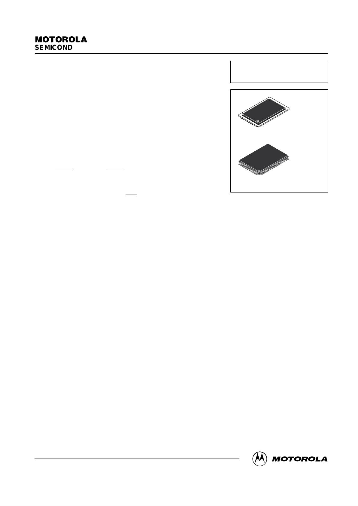
• JEDEC Standard 153–Pin PBGA and 100–Pin TQFP Packages
This document contains information on a new product. Specifications and information herein are subject to change without notice.
Order this document
by MCM63P636/D
MOTOROLA
SEMICONDUCTOR TECHNICAL DATA
MCM63P636
ZP PACKAGE
PBGA
CASE 1107–01
TQ PACKAGE
TQFP
CASE 983A–01
3/16/98
Motorola, Inc. 1998
Page 2
MCM63P636
2
MOTOROLA FAST SRAM
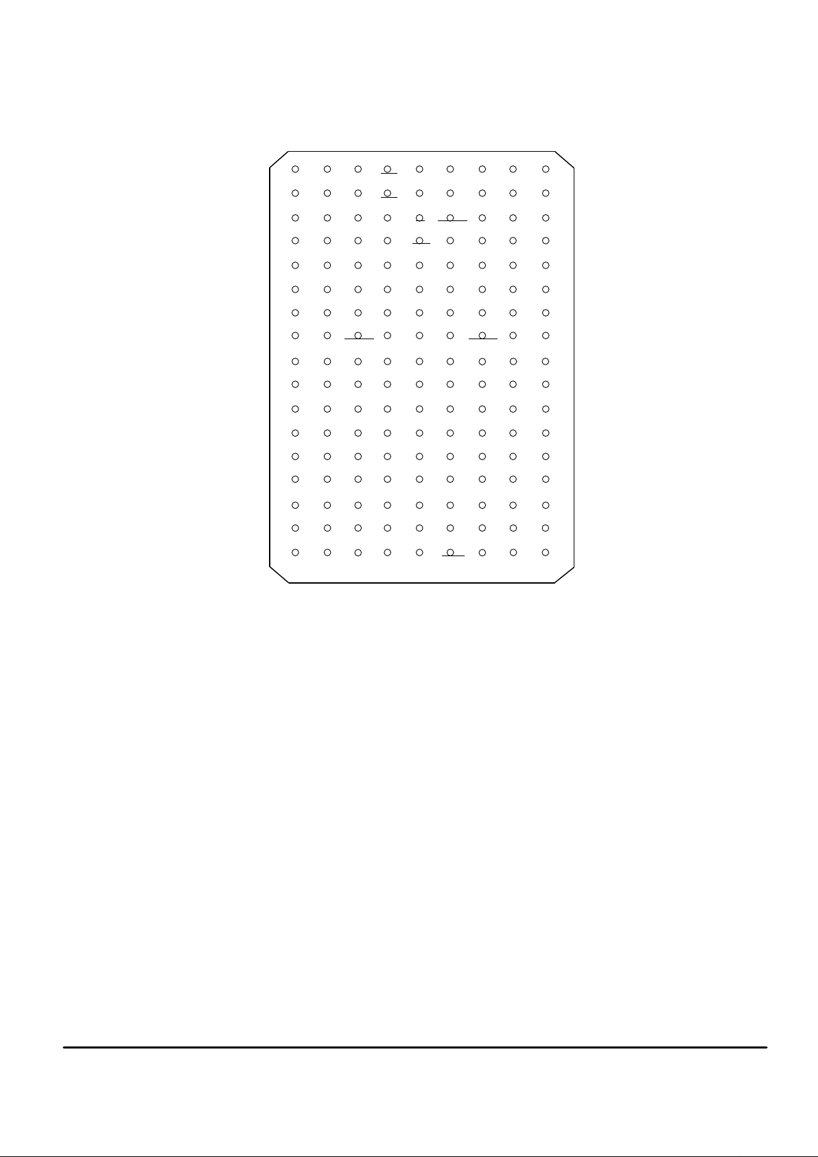
PBGA
PIN ASSIGNMENT
153–BUMP PBGA
TOP VIEW
6543217
B
C
ADS
G
A
D
E
F
H
J
V
SS
K
V
SS
V
SS
NC
SA
SA
SA
V
DDQ
SA SE2 NC
V
SS
W
RESET
DQa SA SA0 SA
SA
V
SS
DQb
V
DDQ
SA
NC
V
DD
V
DD
V
DD
V
DDI
V
SS
STRBB
V
DDI
V
DD
STRBB
DQb
SA1SA
TCK
SA
TDIV
DDQ
DQa
DQa DQa DQa SA
V
SS
V
SS
SA
V
SS
V
SS
V
DD
V
DDQ
V
SS
DQa DQa V
DDI
V
SS
V
DD
V
SS
V
SS
V
DD
V
DDQ
V
SS
DQa DQa STRBA VDDNC
DQa
V
DD
V
SS
NU/V
SS
V
SS
V
SS
V
DDQ
V
SS
DQa STRBA
V
DD
V
DD
V
DD
DQa V
DDIVDD
V
SS
V
SS
V
DD
V
DDQ
V
SS
DQa DQa V
DD
DQa V
DD
NU/V
SS
V
SS
DQa DQa SA SE3
SE1
K
L
M
N
P
R
T
U
V
SS
SA
NU/V
DD
V
SS
V
DDQ
V
SS
89
DQb
DQb
V
SS
DQb
V
DDQ
TDO
DQb
V
SS
V
SS
DQb
V
SS
DQb
DQb
V
SS
DQb
DQbDQb
V
DDQ
DQb
DQb
V
DDQ
DQb
DQb
DQb
V
SS
DQb
V
SS
V
SS
V
DDQ
V
DDQ
V
DDQ
V
DDQ
DQa
VSSV
DDQVDD
SK VSSVDDV
DDQVSS
V
DDQ
TMS TRST
Page 3
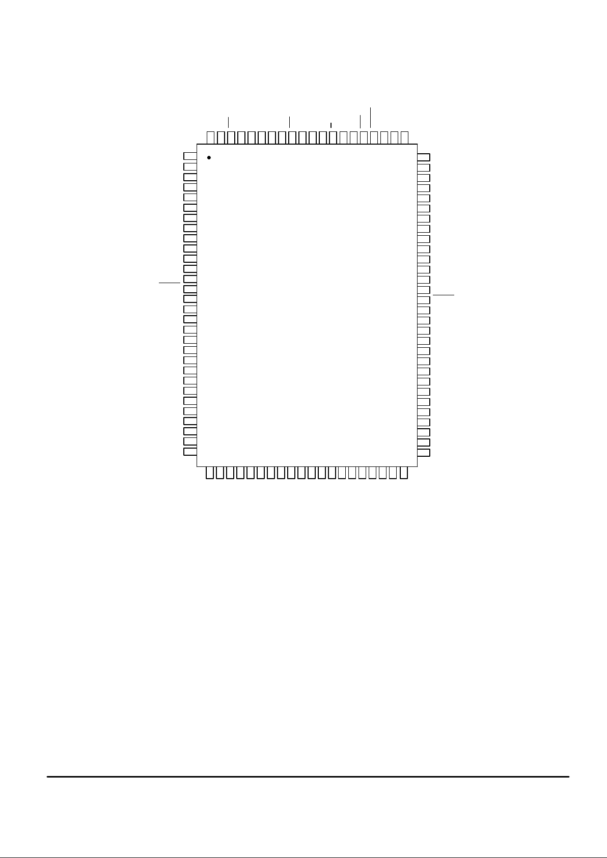
MCM63P636
3
MOTOROLA FAST SRAM
TQFP
PIN ASSIGNMENT
71
72
DQa
DQb
69
70
66
67
68
64
65
61
62
63
37 3834 35 36 42 4339 40 41 45 4644
60
59
58
57
56
55
54
53
52
51
31 32 33
74
75
76
77
78
79
80
50494847
DQb
DQb
V
SS
DQb
DQb
DQb
DQb
V
SS
DQb
DQb
V
DDQ
V
SS
V
SS
DQa
DQa
DQa
DQa
DQa
DQa
DQa
STRBA
SASASE1
K
NU/V
NC
ADS
RESET
SA0
SASASA
SA
NCVNC
DDI
V
SS
NC
SA1
V
DD
V
DD
STRBB
DQb
V
SS
DQb
DQb
DQb
DQb
V
SS
DQb
DQb
V
SS
DQb
DQb
DQa
V
DD
V
SS
V
SS
DQa
DQa
DQa
DQa
DQa
73
DQa
94 9397 96 95 89 8892 91 90 86 8587100 99 98 81828384
10
9
12
11
15
14
13
17
16
20
19
18
21
22
23
24
25
26
27
28
29
30
7
6
5
4
3
2
1
8
SA
SA
V
SE2
SK
SE3
VSSV
DD
W
STRBB
STRBA
V
SS
DQa
DQa
DQa
SA
NC
SASASA
SA
SA
V
DDQ
V
DDQ
V
DDQ
V
DDQ
V
DDQ
V
DDQ
V
DDQ
DDI
V
DDI
V
DDI
DD
NU/VSSNU/V
SS
Page 4
MCM63P636
4
MOTOROLA FAST SRAM
PBGA PIN DESCRIPTIONS
Pin Locations Symbol
Type Description
5D ADS Input Synchronous Address Status: Active low, used to initiate read or write
state machines latch in external addresses, or deselect chip.
(a) 1B, 2B, 1D, 2D, 3D, 1F, 2F, 1H, 2H,
1K, 2K, 1M, 2M, 1P, 2P, 3P, 1T, 2T
(b) 8B, 9B, 7D, 8D, 9D, 8F, 9F, 8H, 9H,
8K, 9K, 8M, 9M, 7P, 8P, 9P, 8T, 9T
DQx I/O Synchronous Data I/O: “x” refers to the word being read or written
(I/Os a and b).
5F K Input Clock: This signal registers the address, data in, and all control signals.
6C RESET Input Asynchronous Power–On Reset: Active low at power up, resets internal
state machines.
3A, 7A, 3B, 7B, 5M, 5N,
4P, 5P, 6P, 4R, 6R, 3T, 4T, 6T
SA Input Synchronous Address Inputs: These inputs are registered and must
meet setup and hold times.
5R, 5T SA1, SA0 Input Synchronous Address Inputs: These pins must be wired to the two
LSBs of the address bus for proper burst operation. These inputs are
registered and must meet setup and hold times.
4A SE1 Input Synchronous Chip Enable: Active low to enable chip.
5A SE2 Input Synchronous Chip Enable: Active high to enable chip.
4B SE3 Input Synchronous Chip Enable: Active low to enable chip.
5G SK Input Data Strobe Clock: 180 degrees out–of–phase with K. Used only with
data strobes.
3K STRBA Output Data Strobe: Used in reference to DQa I/Os.
3H STRBA Output Data Strobe: Used in reference to DQa I/Os.
7K STRBB Output Data Strobe: Used in reference to DQb I/Os.
7H STRBB Output Data Strobe: Used in reference to DQb I/Os.
5U TCK Input Boundary Scan Pin, Test Clock: If boundary scan is not used, TCK
must be tied to VDD or VSS.
3U TDI Input Boundary Scan Pin, T est Data In.
7U TDO Output Boundary Scan Pin, Test Data Out.
4U TMS Input Boundary Scan Pin, Test Mode Select.
6U TRST Input Boundary Scan Pin, Asynchronous T est Reset. If boundary scan is not
used, TRST
must be tied to VSS.
5C W Input Synchronous Write.
4D, 6D, 3E, 7E, 4F, 6F, 3G, 7G,
4H, 6H, 4K, 6K, 3L, 7L, 4M, 6M, 3N, 7N
V
DD
Supply Core Power Supply.
3F, 7F, 3M, 7M V
DDI
Supply Input Power Supply.
2A, 8A, 2C, 8C, 2E, 8E, 2G, 8G,
2J, 8J, 2L, 8L, 2N, 8N, 2R, 8R, 2U, 8U
V
DDQ
Supply I/O Power Supply.
1A, 9A, 1C, 3C, 7C, 9C, 1E, 4E, 5E,
6E, 9E, 1G, 4G, 6G, 9G, 5H, 1J, 3J,
4J, 6J, 7J, 9J, 1L, 4L, 5L, 6L, 9L, 1N,
4N, 6N, 9N, 1R, 3R, 7R, 9R, 1U, 9U
V
SS
Supply Ground.
6A, 5B, 5K, 7T NC — No Connection: There is no connection to the chip.
6B NU/V
DD
— Not Usable: There is an internal connection to the chip. This pin may be
left unconnected or tied to VDD.
4C, 5J NU/V
SS
— Not Usable: There is an internal connection to the chip. This pin may be
left unconnected or tied to VSS.
Page 5
MCM63P636
5
MOTOROLA FAST SRAM
TQFP PIN DESCRIPTIONS
Pin Locations Symbol
Type Description
85 ADS Input Synchronous Address Status: Active low, used to initiate read or write
state machines latch in external addresses, or deselect chip.
(a) 1, 2, 3, 6, 7, 8, 9, 12, 13, 18,
19, 22, 23, 24, 25, 28, 29, 30
(b) 51, 52, 53, 56, 57, 58, 59, 62, 63,
68, 69, 72, 73, 74, 75, 78, 79, 80
DQx I/O Synchronous Data I/O: “x” refers to the word being read or written
(I/Os a and b).
89 K Input Clock: This signal registers the address, data in, and all control signals.
84 RESET Input Asynchronous Power–On Reset: Active low at power up, resets internal
state machines.
32, 33, 34, 35, 44, 45, 46,
47, 48, 49, 81, 82, 99, 100
SA Input Synchronous Address Inputs: These inputs are registered and must
meet setup and hold times.
36, 37 SA1, SA0 Input Synchronous Address Inputs: These pins must be wired to the two
LSBs of the address bus for proper burst operation. These inputs are
registered and must meet setup and hold times.
98 SE1 Input Synchronous Chip Enable: Active low to enable chip.
97 SE2 Input Synchronous Chip Enable: Active high to enable chip.
92 SE3 Input Synchronous Chip Enable: Active low to enable chip.
93 SK Input Data Strobe Clock: 180 degrees out–of–phase with K. Used only with
data strobes.
16 STRBA Output Data Strobe: Used in reference to DQa I/Os.
14 STRBA Output Data Strobe: Used in reference to DQa I/Os.
64 STRBB Output Data Strobe: Used in reference to DQb I/Os.
66 STRBB Output Data Strobe: Used in reference to DQb I/Os.
88 W Input Synchronous Write.
15, 41, 65, 91 V
DD
Supply Core Power Supply.
38, 43, 87, 94 V
DDI
Supply Input Power Supply.
4, 11, 20, 27, 54, 61, 70, 77 V
DDQ
Supply I/O Power Supply.
5, 10, 17, 21, 26, 40,
55, 60, 67, 71, 76, 90
V
SS
Supply Ground.
31, 39, 42, 50, 86 NC — No Connection: There is no connection to the chip.
83 NU/V
DD
— Not Usable: There is an internal connection to the chip. This pin may be
left unconnected or tied to VDD.
95, 96 NU/V
SS
— Not Usable: There is an internal connection to the chip. This pin may be
left unconnected or tied to VSS.
Page 6
MCM63P636
6
MOTOROLA FAST SRAM
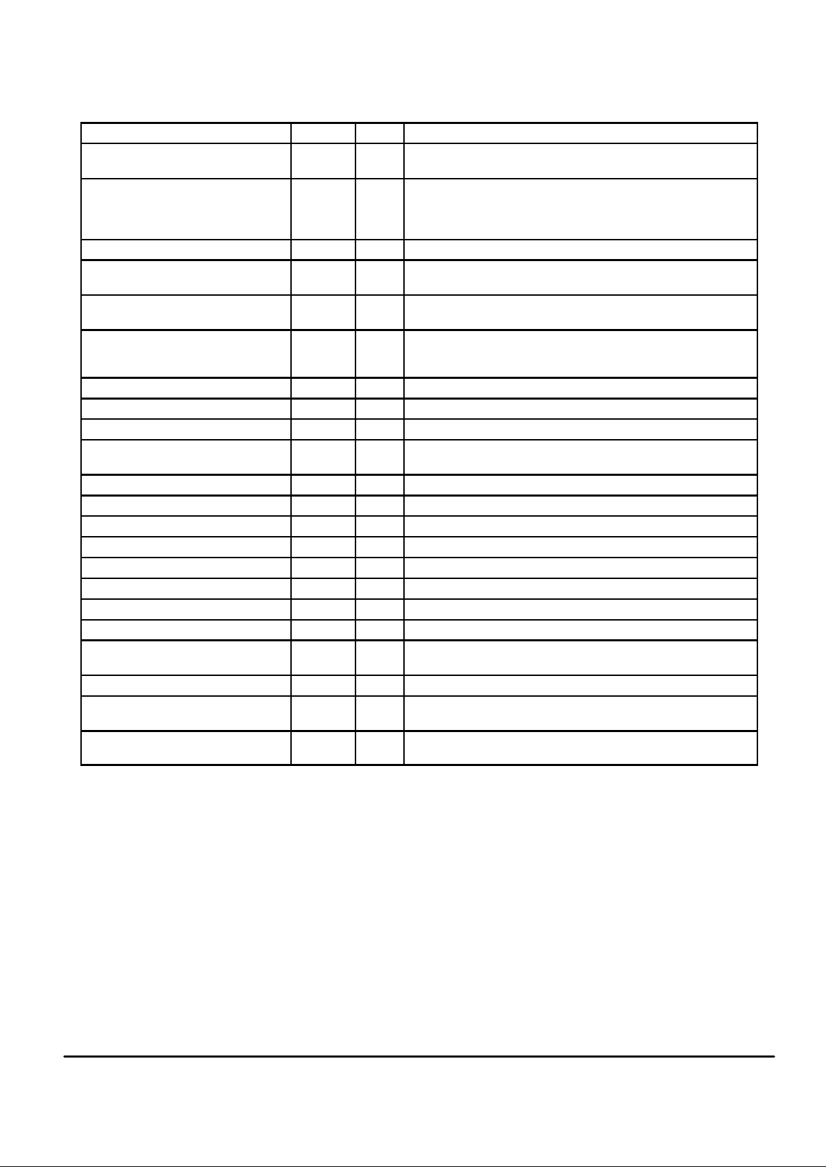
TRUTH TABLE (See Notes 1 and 2)
K
E ADS W Next Cycle (n) Input Command Code DQ (n + 1) DQ (n+2)
L – H False 0 X Deselect D High–Z —
L – H True 0 0 Load Address, Begin Write BW Data In —
L – H True 0 1 Load Address, Begin Read BR — Data Out
L – H X 1 0 Continue W rite CW Data In —
L – H X 1 1 Continue Read
Mask Write
CR
MW
—
High–Z
Data Out
—
NOTES:
1. X = don’t care, 1 = logic high, 0 = logic low.
2. E = true if SE1
and SE3 = 0, and SE2 = 1.
BURST ADDRESS TABLE
1st Address (External) 2nd Address (Internal) 3rd Address (Internal) 4th Address (Internal)
X . . . X00 X . . . X01 X . . . X10 X . . . X11
X . . . X01 X . . . X00 X . . . X1 1 X . . . X10
X . . . X10 X . . . X11 X . . . X00 X . . . X01
X . . . X11 X . . . X10 X . . . X01 X . . . X00
DESELECT
NEW
READ*
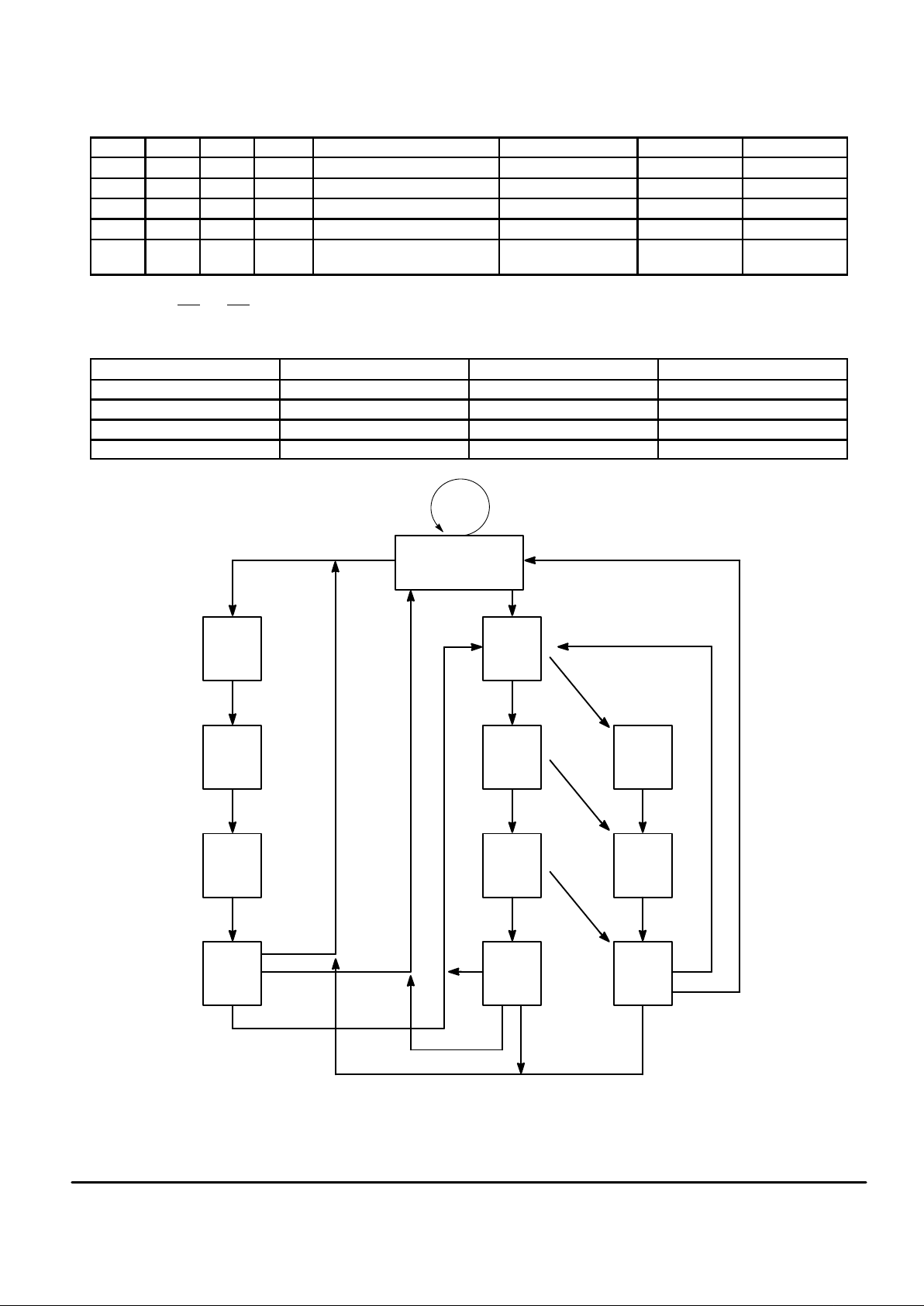
Figure 1. Functional State Diagram
BURST
READ 1*
BURST
READ 2*
BURST
READ 3*
NEW
WRITE*
BURST
WRITE 1*
BURST
WRITE 2*
BURST
WRITE 3*
MASKED
WRITE 1*
MASKED
WRITE 2*
MASKED
WRITE 3*
D, CW, CR – MW
BR
BW
CR
CR
CR
BR
BW
BW
D, CW, MW
CW
CW
CW
BR
MW
MW
MW
MW
MW
BR
BW
D, CW, MW
D, CW, MW
*Command code inputs not shown from this state are not valid.
Page 7
MCM63P636
7
MOTOROLA FAST SRAM
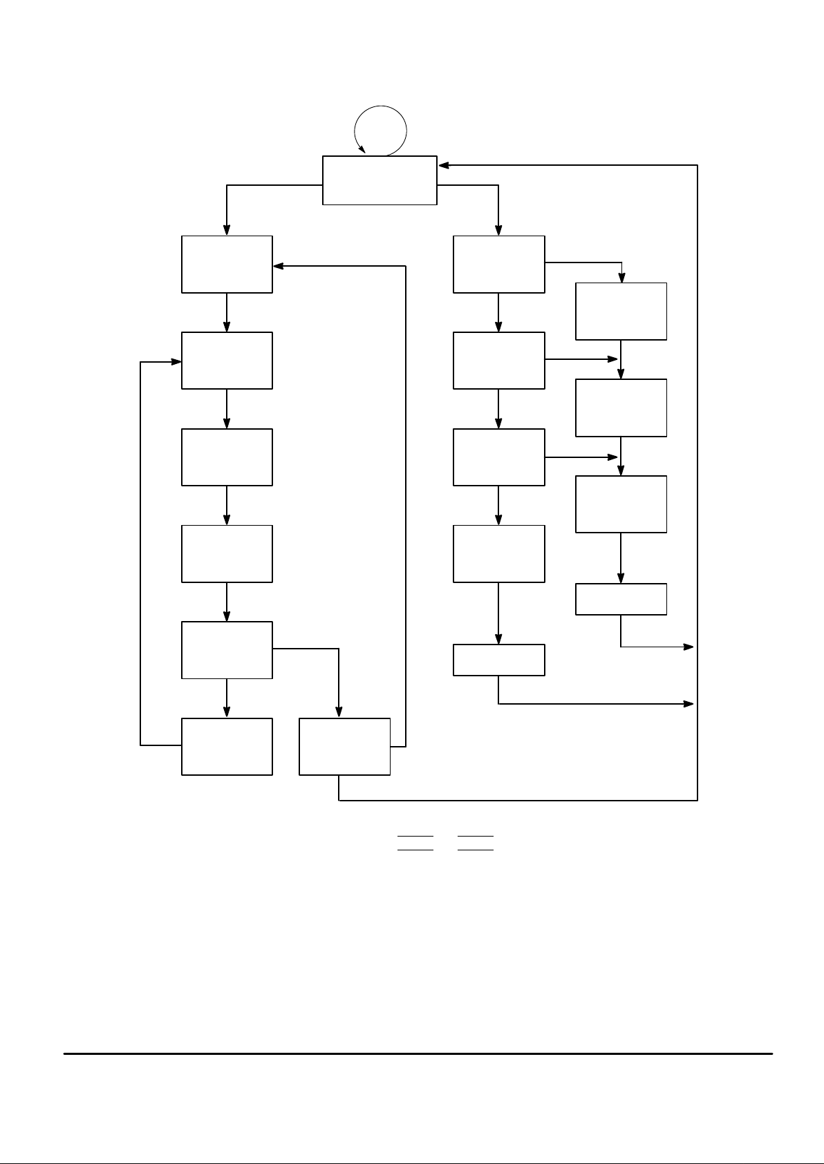
HIGH–Z
4
INTERMEDIATE
HIGH–Z1,
4
Figure 2. Data I/O State Diagram
D, CW, CR – MW
BR
CR
CR
CR
D, CW, CR
CW, MW
MW
CW, MW
NOTES:
1. Command code inputs not shown from this state are not valid.
2. STRBA and STRBB transition from logic 1 to 0. STRBA
and STRBB transition from logic 0 to 1.
3. STRBA and STRBB transition from logic 0 to 1. STRBA
and STRBB transition from logic 1 to 0.
4. Data strobes are driven to High–Z.
INTERMEDIA TE
HIGH–Z1,
4
DATA–OUT/
Q(1)VALID1,
2
DATA–OUT/
Q(2)VALID1,
3
DATA–OUT/
Q(3)VALID1,
2
DATA–OUT/
Q(4)VALID1,
3
DATA–OUT/
Q(4)VALID1,
3
DATA–IN (1)/
HIGH–Z1,
4
CW
CW
CW
DATA–IN (2)/
HIGH–Z1,
4
DATA–IN (3)/
HIGH–Z1,
4
DATA–IN (4)/
HIGH–Z1,
4
MASK (2)/
HIGH–Z1,
4
MW
MW
MW
MASK (3)/
HIGH–Z1,
4
MASK (4)/
HIGH–Z1,
4
HIGH–Z1,
4
MW
MW
MW
HIGH–Z1,
4
BR
CR
BR
CR
BW
CR
Page 8
MCM63P636
8
MOTOROLA FAST SRAM
ABSOLUTE MAXIMUM RATINGS (See Note 1)
Rating Symbol Value Unit Notes
Power Supply Voltage V
DD
VSS – 0.5 to + 4.0 V
I/O Supply Voltage V
DDQ
VSS – 0.5 to 2.5 V 2, 3
Input Supply Voltage V
DDI
VSS – 0.5 to 2.5 V 2, 3
Voltage Relative to VSS for Any Pin
Except V
DD
V
in
VSS – 0.5 to
V
DDI
+ 0.5
V 2, 4
Input Voltage (Three–State I/O) V
IT
VSS – 0.5 to
V
DDQ
+ 0.5
V 2, 4
Output Current (per I/O) I
out
± 20 mA
Package Power Dissipation P
D
2.75 W 5
Temperature Under Bias T
bias
– 10 to 85 °C
Storage Temperature T
stg
– 55 to 125 °C
NOTES:
1. Permanent device damage may occur if ABSOLUTE MAXIMUM RATINGS are
exceeded. Functional operation should be restricted to RECOMMENDED OPERATING CONDITIONS. Exposure to higher than recommended voltages for extended
periods of time could affect device reliability.
2. This is a steady–state DC parameter that is in effect after the power supply has
achieved its nominal operating level. Power sequencing is not necessary.
3. V
DDI
= V
DDQ
.
4. Max Vin and VIT are not to exceed Max VDD.
5. Power dissipation capability is dependent upon package characteristics and use
environment. See Package Thermal Characteristics.
PACKAGE THERMAL CHARACTERISTICS — PBGA
Rating Symbol Max Unit Notes
Junction to Ambient (@ 200 lfm) R
θJA
25 °C/W 1, 2
Junction to Board (Bottom) R
θJB
12 °C/W 3
Junction to Case (Top) R
θJC
10 °C/W 4
PACKAGE THERMAL CHARACTERISTICS — TQFP
Rating Symbol Max Unit Notes
Junction to Ambient (@ 200 lfm) R
θJA
25 °C/W 1, 2
Junction to Board (Bottom) R
θJB
17 °C/W 3
Junction to Case (Top) R
θJC
9 °C/W 4
NOTES:
1. Junction temperature is a function of on–chip power dissipation, package thermal resistance, mounting site (board) temperature, ambient
temperature, air flow, and board thermal resistance.
2. Per SEMI G38–87.
3. Indicates the average thermal resistance between the die and the printed circuit board.
4. Indicates the average thermal resistance between the die and the case top surface via the cold plate method (MIL SPEC–883 Method 1012.1).
This device contains circuitry to protect the
inputs against damage due to high static voltages or electric fields; however, it is advised
that normal precautions be taken to avoid
application of any voltage higher than maximum rated voltages to this high–impedance
circuit.
Page 9
MCM63P636
9
MOTOROLA FAST SRAM
DC OPERA TING CONDITIONS AND CHARACTERISTICS
(VDD = 3.3 V ± 200 mV, TA = 0 to 70°C, Unless Otherwise Noted)
RECOMMENDED OPERATING CONDITIONS AND DC CHARACTERISTICS (Voltage Referenced to V
SS
= 0 V)
Parameter Symbol Min Typ Max Unit
Supply Voltage V
DD
3.1 3.3 3.5 V
Input Supply Voltage V
DDI
1.8 — 2.2 V
I/O Supply Voltage V
DDQ
1.8 — 2.2 V
Input Low Voltage (V
DDI
= V
DDQ
) V
IL
– 0.5 — 0.35 x V
DDI
V
Input High Voltage (V
DDI
= V
DDQ
) V
IH
0.65 x V
DDI
— V
DDI
+ 0.5 V
Input Leakage Current (0 V ≤ Vin ≤ VDD) I
lkg(I)
— — ± 1 µA
Output Leakage Current (0 V ≤ Vin ≤ V
DDQ
) I
lkg(O)
— — ± 1 µA
Output Low Voltage (IOL = 1 mA) V
OL
– 0.5 — 0.4 V
Output High Voltage (IOL = – 1 mA) V
OH
V
DDQ
– 0.4 — V
DDQ
+ 0.5 V
V
IH
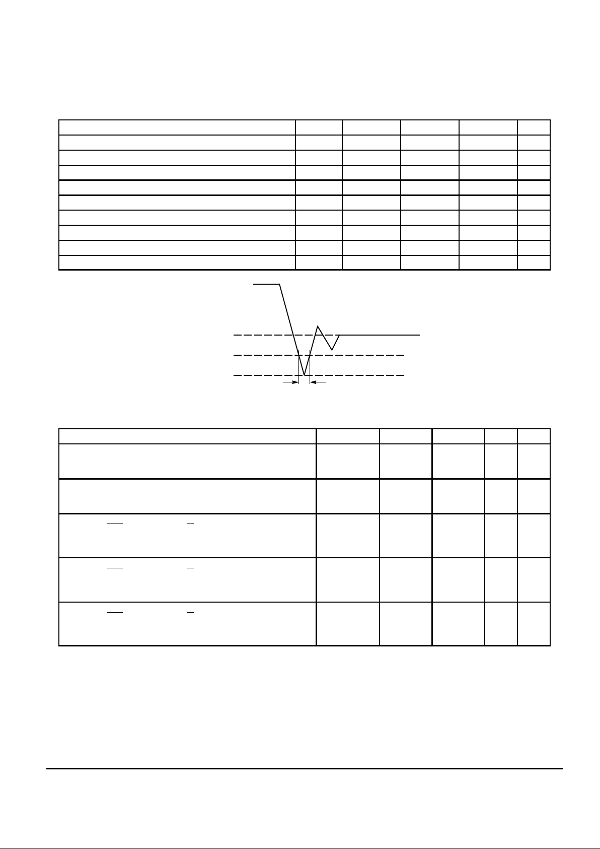
20% t
KHKH
V
SS
VSS – 0.5 V
Figure 3. Undershoot Voltage
VSS – 0.25 V
SUPPLY CURRENTS
Parameter Symbol Min Max Unit Notes
AC Supply Current (Device Selected, All Outputs Open,
Freq = Max, VDD = Max)
I
DDA
– 250
I
DDA
– 225
I
DDA
– 200
— TBD mA 1, 2,
3, 4
Input and I/O Supply Current – Desktop (All 40 Outputs Toggling,
Freq = Max, V
DDI
= Max, V
DDQ
= Max, V
DDI
= V
DDQ
, Cdt = 24 pF)
I
DDQ
– 250
I
DDQ
– 225
I
DDQ
– 200
— 311
280
249
mA 2, 5
Static Standby Supply Current (Device Deselected, Freq = Max,
VDD = Max, ADS
≥ (V
DDI
– 0.2 V), W Static ≤ (VSS + 0.2 V)
or ≥ (V
DDI
– 0.2 V), SA and DQx Inputs Static ≤ (VSS + 0.2 V),
Outputs Disabled)
I
SB1
– 250
I
SB1
– 225
I
SB1
– 200
— 63
57
50
mA 1, 2, 4
Idle Standby Supply Current (Device Deselected, Freq = 0,
VDD = Max, ADS
≥ (V
DDI
– 0.2 V), W Static ≤ (VSS + 0.2 V)
or ≥ (V
DDI
– 0.2 V), SA and DQx Inputs Static ≤ (VSS + 0.2 V),
Outputs Disabled)
I
SB2A
— TBD mA 1, 3, 4
Idle Input Standby Supply Current (Device Deselected, Freq = 0,
VDD = Max, ADS
≥ (V
DDI
– 0.2 V), W Static ≤ (VSS + 0.2 V)
or ≥ (V
DDI
– 0.2 V), SA and DQx Inputs Static ≤ (VSS + 0.2 V),
Outputs Disabled)
I
SB2B
— TBD mA 1, 3, 5
NOTES:
1. Device is selected and deselected as defined by the Truth Table.
2. Reference AC Operating Conditions and Characteristics for input and timing.
3. Data states are all zero.
4. Includes supply current for VDD only.
5. Includes supply currents for V
DDI
and V
DDQ
only.
Page 10

MCM63P636
10
MOTOROLA FAST SRAM
CAPACITANCE AND INDUCTANCE (See Notes 1, 2, and 3)
TQFP PBGA
Capacitance (pF) Inductance (nH) Capacitance (pF) Inductance (nH)
Pin Description
Min Max Min Max Min Max Min Max
I/O Pins 5 7 2 10 5.5 7.5 2.5 4.5
Data Strobe Pins 5 7 2 10 5.5 7.5 2.5 4.5
Input Pins 3 5 2 10 3.5 5.5 2.5 4
ADS Pin 5 7 2 10 5.5 7.5 2.5 4.5
K and SK Pins 3.5 4.5 2 10 4 5 1.5 3
TCK Boundary Scan Pin — — — — — 5 — —
Boundary Scan Input Pins — — — — — 8 — —
TDO Boundary Scan Pin — — — — — 8 — —
NOTES:
1. Parameters are periodically sampled rather than 100% tested.
2. Capacitance variation part to part on the same pin is ± 0.25 pF.
3. Inductance variation part to part on the same pin is ± 1 nH.
AC OPERA TING CONDITIONS AND CHARACTERISTICS
(VDD = 3.3 V ± 200 mV, Unless Otherwise Noted)
AC TEST CONDITIONS
Parameter Value Unit
Input Timing Reference Level V
DDQ
/2 V
Input Pulse Levels 0 to 2.0 V
Input Rise/Fall Time (20 to 80%) 1 V/ns
Output Timing Reference Level V
DDQ
/2 V
Die Temperature TJ–250
TJ–225
TJ–200
115
115
115
°C
OUTPUT
R
L
Figure 4. AC Output Test Load
Z0 = 50
Ω
1.0 V
Figure 5. Lumped Capacitive Load and Typical Derating Curve
(TBD)
Page 11

MCM63P636
11
MOTOROLA FAST SRAM
READ/WRITE CYCLE TIMING (See Notes 1 and 2)
MCM63P636–250 MCM63P636–225 MCM63P636–200
Parameter Symbol
Min Max Min Max Min Max
Unit Notes
Clock Cycle Time t
KHKH
4 — 4.4 — 5 — ns 3, 4
Clock High Time t
KH
1.06 — 1.24 — 1.46 — ns 4
Clock Low Time t
KL
1.06 — 1.24 — 1.46 — ns 4
Strobe Clock Cycle Time t
SKHSKH
4 — 4.4 — 5 — ns 3, 4
Strobe Clock High Time t
SKH
1.06 — 1.24 — 1.46 — ns 4
Strobe Clock Low Time t
SKL
1.06 — 1.24 — 1.46 — ns 4
Rising K to Rising SK t
KHSKH
1.6 2.4 1.8 2.6 2.1 2.9 3
Clock Access Time t
KHQV
— 3.9 — 4.3 — 4.9 ns 3
Clock to Output Low–Z t
KHQX
0 — 0 — 0 — ns 5, 6
Clock to Output High–Z t
KHQZ
— 3.9 — 4.3 — 4.9 ns 5, 6
Strobe Clock Access Time t
SKHSTV
— 3.9 — 4.3 — 4.9 ns 3
Setup Times: Address
ADS
Chip Enable
Data In
Data Out
Write
t
AVKH
t
SVKH
t
EVKH
t
DVKH
t
QVSTV
t
WVKH
0.5
1.2
0.5
1.2
1
1.2
— 0.5
1.5
0.5
1.5
1.1
1.5
— 0.5
1.5
0.5
1.5
1.15
1.5
— ns 3
Hold Times: Address
ADS
Chip Enable
Data In
Data Out
Write
t
KHAX
t
KHSX
t
KHEX
t
KHDX
t
STVQX
t
KHWX
4
0.5
4
0.5
1
0.5
— 4.4
0.5
4.4
0.5
1.1
0.5
— 5
0.5
5
0.5
1.15
0.5
— ns 3
NOTES:
1. Reads and writes are as defined in the Truth Table.
2. All read and write cycle timings are referenced from K, SK, or data strobes.
3. In order to reduce test correlation issues and to reduce the effects of application specific input edge rate variations on correlation between
data sheet parameters and actual system performance, FSRAM AC parametric specifications are always specified at V
DDQ
/2. In some
design exercises, it is desirable to evaluate timing using other reference levels. Since the maximum test input edge rate is known and is
given in the AC Test Conditions section of the data sheet as 1 V/ns, one can easily interpolate timing values to other reference levels.
4. Refer to Figure 5 for input reference levels.
5. This parameter is sampled and not 100% tested.
6. Measured at
± 200 mV from steady state.
V
IH
V
IL
V
DDQ
V
SS
V
DDQ
/2
tKH, t
SKH
tKL, t
SKL
t
KHKH
, t
SKHSKH
Figure 6. AC Timing Diagram Clock Reference
Page 12

MCM63P636
12
MOTOROLA FAST SRAM
(a) Pull–Up
VOLTAGE (V)
PULL–UP
I (mA) MIN I (mA) MAX
– 0.5
0
0.2
0.4
0.6
0.8
1
1.2
– 32
– 32
– 32
– 28
– 24
– 20
– 16
– 12
– 72
– 72
– 72
– 72
– 64
– 56
– 48
– 40
2.2
1.8
1.6
0.6
0
0– 72
CURRENT (mA)
VOLTAGE (V)
1.4
1.6
– 8
– 4
– 32
– 24
– 32
0.2
1.8
2
2.2
0
4
8
– 16
– 8
0
(b) Pull–Down
VOLTAGE (V)
PULL–UP
I (mA) MIN I (mA) MAX
– 0.5
0
0.2
0.4
0.6
0.8
1
1.2
– 10
0
4
8
12
16
20
24
– 20
0
8
16
24
32
40
48
V
DDQ
1.8
1.4
0.6
0
072
CURRENT (mA)
VOLTAGE (V)
1.4
1.6
28
28
56
64
28
0.2
1.8
2
2.2
28
28
28
72
72
72
Figure 7. Typical Output Buffer Characteristics – PBGA Only
Page 13

MCM63P636
13
MOTOROLA FAST SRAM
(a) Pull–Up
VOLTAGE (V)
PULL–UP
I (mA) MIN I (mA) MAX
– 0.5
0
0.2
0.4
0.6
0.8
1
1.2
– 23
– 23
– 23
– 20
– 17
– 14
– 11
– 9
– 60
– 60
– 60
– 60
– 53
– 47
– 40
– 33
2.2
1.8
1.6
0.6
0
0– 60
CURRENT (mA)
VOLTAGE (V)
1.4
1.6
– 6
– 3
– 27
– 20
– 23
0.2
1.8
2
2.2
0
3
6
– 13
– 7
0
(b) Pull–Down
VOLTAGE (V)
PULL–UP
I (mA) MIN I (mA) MAX
– 0.5
0
0.2
0.4
0.6
0.8
1
1.2
– 7
0
3
6
9
11
14
17
– 17
0
7
13
20
27
33
40
V
DDQ
1.8
1.4
0.6
0
060
CURRENT (mA)
VOLTAGE (V)
1.4
1.6
20
20
47
53
20
0.2
1.8
2
2.2
20
20
20
60
60
60
Figure 8. Typical Output Buffer Characteristics – TQFP Only
Page 14

MCM63P636
14
MOTOROLA FAST SRAM
W
t
AVKH
SK
K
ADS
E
Q(A)
SA A
READ CYCLES
t
KHAX
DQx
STRBA/B
B
Q(A +1) Q(A + 2) Q(A + 3) Q(B) Q(B + 1) Q(B + 2) Q(B + 3)
t
STVQX
STRBA/B
t
SVKH
t
KHSX
t
WVKH
t
KHWX
t
EVKH
t
KHEX
t
KHQX
t
KHQV
t
QVSTV
t
SKHSTV
t
KHQZ
NOTE: E low = SE1 and SE3 low and SE2 high.
Page 15

MCM63P636
15
MOTOROLA FAST SRAM
W
SK
K
ADS
E
D(A)
SA A
WRITE CYCLES
DQx
STRBA/B
B
D(A + 1) D(A + 2) D(A + 3) D(B) D(B + 1)
STRBA/B
t
DVKH
t
KHSKH
t
KHDX
HIGH–Z
Page 16

MCM63P636
16
MOTOROLA FAST SRAM
W
SK
K
ADS
E
Q(A)
SA
A
READ/WRITE CYCLES
DQx
STRBA/B
B
Q(A +1) Q(A + 2) Q(A + 3) D(B) D(B + 1) D(B + 2) D(B + 3)
STRBA/B
C
Q(C) Q(C + 1) Q(C + 2) Q(C + 3)
BURST READ BURST WRITE BURST READ DESELECT
Page 17

MCM63P636
17
MOTOROLA FAST SRAM
FUNCTIONAL OPERATION
POWER UP AND INITIALIZATION
The RESET
input is used to reset the SRAM internal logic
at power on. At power on, this pin is held low and then driven
high at some later time. Eight cycles after the RESET
is as-
serted high, standard SRAM functionality may begin.
DATA STROBES
The data strobes STRBA, STRBA
, STRBB, and STRBB
are driven by the SRAM to be used by the device receiving
the output data. The data strobes toggle only at the approximate center of each output data valid window such that the
external device can reliably latch in this data. Following a
burst read, the data strobes will be driven to High–Z.
WRITE CYCLES
The address is sampled on the first rising edge of clock of
each burst write sequence, and the write data is sampled on
the subsequent rising clock edges. During a burst write the
last, last two, or last three addresses may be blocked from
being written by asserting the W
synchronous write pin high.
However, once W is asserted high, it must remain in this
state through the remainder of the burst write sequence. All
burst write (and masked write) sequences must be followed
by an inactive cycle to reset internal state machines.
LOW POWER STOP–CLOCK OPERATION
In the stop–clock mode of operation, the SRAM will hold all
state and data values even though the clock is not running
(full static operation). The SRAM design allows the clock to
start with ADS
, and stops the clock after the last write data is
latched, or the last read data is driven out.
When starting and stopping the clock, the initial clocks being driven may not meet the AC clock timing parametrics, but
will meet those parametrics at least two clocks prior to ADS
being asserted low.
To achieve the lowest power operation for all three stop
clock modes, stop read, stop write, and stop deselect:
• Force the clock to a low state.
• Force the control signals to an inactive state (this guar-
antees any potential source of noise on the clock input
will not start an unplanned on activity).
• Force the address inputs to a low state (VIL), preferably
< 0.2 V.
V
IL
K
ADS
SA
D
in
Q
out
A B
V
IH
V
IL
V
IL
HIGH–ZHIGH–Z
STOP–CLOCK WITH READ TIMING
ADS
INITIATES
BURST READ
END
BURST
READ
K
CLOCK
STOP
STOP–CLOCK
LOW POWER
OPERATION
WAKE–UP/
INVALID
CLOCK
INVALID
CLOCK
FIRST
VALID
CLOCK
Q(A) Q(A +1) Q(A +2) Q(A +3)
Page 18

MCM63P636
18
MOTOROLA FAST SRAM
V
IL
K
ADS
SA
D
in
Q
out
A B
V
IH
V
IL
HIGH–Z
STOP–CLOCK WITH WRITE TIMING
ADS
INITIATES
BURST WRITE
END
BURST
WRITE
K
CLOCK
STOP
STOP–CLOCK
LOW POWER
OPERATION
WAKE–UP/
INVALID
CLOCK
INVALID
CLOCK
FIRST
VALID
CLOCK
W
V
IH
HIGH–Z
V
IL
D(A) D(A +1) D(A +2) D(A +3)
V
IL
K
ADS
SA
D
in
Q
out
A
V
IH
V
IL
STOP–CLOCK WITH DESELECT TIMING
CONTINUE
BURST
READ
END
READ/
DESELECT
K
CLOCK
STOP
STOP–CLOCK
LOW POWER
OPERATION
WAKE–UP/
INVALID
CLOCK
INVALID
CLOCK
FIRST
VALID
CLOCK
E
HIGH–Z
V
IL
Q(3) Q(4)
Page 19

MCM63P636
19
MOTOROLA FAST SRAM
SERIAL BOUNDARY SCAN TEST ACCESS PORT OPERATION
OVERVIEW
The serial boundary scan test access port (TAP) on this
RAM is designed to operate in a manner consistent with
IEEE Standard 1149.1–1990 (commonly referred to as
JTAG), but does not implement all of the functions required
for IEEE 1149.1 compliance. Certain functions have been
modified or eliminated because their implementation places
extra delays in the RAMs critical speed path. Nevertheless,
the RAM supports the standard TAP controller architecture
(the TAP controller is the state machine that controls the
TAPs operation) and can be expected to function in a manner
that does not conflict with the operation of devices with IEEE
Standard 1149.1 compliant TAPs. The TAP operates using a
2.5 V tolerant logic level signaling.
DISABLING THE TEST ACCESS PORT
It is possible to use this device without utilizing the TAP. To
disable the TAP controller without interfering with normal
operation of the device, TRST
should be tied low and TCK,
TDI, and TMS should be pulled through a resistor to 2.0 V.
TDO should be left unconnected.
T AP DC OPERATING CHARACTERISTICS
(TA = 0 to 70°C, Unless Otherwise Noted)
Parameter
Symbol Min Max Unit Notes
Input Logic Low VIL1 – 0.5 0.35 x V
DDQ
V
Input Logic High VIH1 0.65 x V
DDQ
2.5 V
Input Leakage Current I
lkg
— ± 10 µA 1
Output Logic Low VOL1 VSS – 0.5 0.4 V 2
Output Logic High VOH1 V
DDQ
– 0.4 V
DDQ
+ 0.5 V
NOTES:
1. 0 V ≤ Vin ≤ V
DDQ
for all logic input pins.
2. For VOL = 0.4 V, 14 mA ≤ IOL ≤ 28 mA.
Page 20

MCM63P636
20
MOTOROLA FAST SRAM
T AP AC OPERATING CONDITIONS AND CHARACTERISTICS
(TA = 0 to 70°C, Unless Otherwise Noted)
AC TEST CONDITIONS
Parameter Value Unit
Input Timing Reference Level V
DDQ
/2 V
Input Pulse Levels 0 to 2.0 V
Input Rise/Fall Time (20 to 80%) 1 V/ns
Output Timing Reference Level V
DDQ
/2 V
Output Load (See Figure 4 Unless Otherwise Noted) — —
TAP CONTROLLER TIMING
Parameter Symbol Min Max Unit Notes
TCK Cycle Time t
THTH
60 — ns
TCK Clock High Time t
TH
25 — ns
TCK Clock Low Time t
TL
25 — ns
TDO Access Time t
TLQV
1 10 ns
TRST Pulse Width t
TSRT
40 — ns
Setup Times Capture
TDI
TMS
t
CS
t
DVTH
t
MVTH
5
5
5
— ns 1
Hold Times Capture
TDI
TMS
t
CH
t
THDX
t
THMX
13
14
14
— ns 1
NOTE:
1. tCS and tCH define the minimum pauses in RAM I/O transitions to assure accurate pad data capture.
t
THDX
t
TLQV
t
DVTH
t
TLTH
t
THMX
t
MVTH
TAP CONTROLLER TIMING DIAGRAM
t
THTH
TEST CLOCK
(TCK)
TEST MODE SELECT
(TMS)
TEST DATA IN
(TDI)
TEST DATA OUT
(TDO)
t
THTL
Page 21

MCM63P636
21
MOTOROLA FAST SRAM
Boundary Scan Order
Bit
No.
Signal
Name
Bump
ID
1 DQa 3D
2 DQa 1B
3 DQa 2B
4 DQa 1D
5 DQa 2D
6 DQa 1F
7 DQa 2F
8 DQa 1H
9 DQa 2H
10 STRBA* 3H
11 STRBA* 3K
12 DQa 2K
13 DQa 1K
14 DQa 2M
15 DQa 1M
16 DQa 2P
17 DQa 1P
18 DQa 2T
19 DQa 1T
20 DQa 3P
21 SA 3T
22 SA 4P
23 SA 4R
24 SA 4T
25 SA1 5R
26 SA0 5T
27 SA 5M
28 SA 5N
29 SA 5P
30 SA 6P
31 SA 6R
32 SA 6T
33 NC* 7T
Bit
No.
Signal
Name
Bump
ID
34 DQb 7P
35 DQb 8T
36 DQb 9T
37 DQb 9P
38 DQb 8P
39 DQb 9M
40 DQb 8M
41 DQb 9K
42 DQb 8K
43 STRBB* 7K
44 STRBB 7H
45 DQb 8H
46 DQb 9H
47 DQb 8F
48 DQb 9F
49 DQb 8D
50 DQb 9D
51 DQb 8B
52 DQb 9B
53 DQb 7D
54 SA 7A
55 SA 7B
56 RESET 6C
57 ADS 5D
58 W 5C
59 K 5F
60 SE3 4B
61 SK 5G
62 NU/V
SS
5J
63 SE2 5A
64 SE1 4A
65 SA 3A
66 SA 3B
*Scans as logic 0.
Page 22

MCM63P636
22
MOTOROLA FAST SRAM
TEST ACCESS PORT PINS
TCK — TEST CLOCK (INPUT)
Clocks all TAP events. All inputs are captured on the rising
edge of TCK and all outputs propagate from the falling edge
of TCK.
TMS — TEST MODE SELECT (INPUT)
The TMS input is sampled on the rising edge of TCK. This
is the command input for the TAP controller state machine.
An undriven TMS input will not produce the same result as a
logic one input level (not IEEE 1149.1 compliant).
TDI — TEST DATA IN (INPUT)
The TDI input is sampled on the rising edge of TCK. This is
the input side of the serial registers placed between TDI and
TDO. The register placed between TDI and TDO is determined by the state of the TAP controller state machine and
the instruction that is currently loaded in the TAP instruction
register (refer to Figure 10, TAP Controller State Diagram).
An undriven TDI pin will not produce the same result as a
logic one input level (not IEEE 1149.1 compliant).
TDO — TEST DATA OUT (OUTPUT)
Output that is active depending on the state of the TAP
state machine (refer to Figure 10, TAP Controller State Diagram). Output changes in response to the falling edge of
TCK. This is the output side of the serial registers placed
between TDI and TDO.
TRST
— TAP RESET
The TRST
is an asynchronous input that resets the TAP
controller and pre–loads the instruction register with the
IDCODE command. This type of reset does not affect the
operation of the system logic. The reset affects test logic
only.
TEST ACCESS PORT REGISTERS
OVERVIEW
The various TAP registers are selected (one at a time) via
the sequences of ones and zeros input to the TMS pin as the
TCK is strobed. Each of the TAPs registers are serial shift
registers that capture serial input data on the rising edge of
TCK and push serial data out on subsequent falling edge of
TCK. When a register is selected it is “placed” between the
TDI and TDO pins.
INSTRUCTION REGISTER
The instruction register holds the instructions that are
executed by the TAP controller when it is moved into the run
test/idle or the various data register states. The instructions
are three bits long. The register can be loaded when it is
placed between the TDI and TDO pins. The parallel outputs
of the instruction register are automatically preloaded with
the IDCODE instruction when TRST
is asserted or whenever
the controller is placed in the test–logic–reset state. The two
least significant bits of the serial instruction register are
loaded with a binary “or” pattern in the capture–IR state.
BYPASS REGISTER
The bypass register is a single bit register that can be
placed between TDI and TDO. It allows serial test data to be
passed through the RAMs TAP to another device in the scan
chain with as little delay as possible.
BOUNDARY SCAN REGISTER
The boundary scan register is identical in length to the
number of active input and I/O connections on the RAM (not
counting the T AP pins). This also includes a number of place
holder locations (always set to a logic 0) reserved for density
upgrade address pins. There are a total of 66 bits in the case
of the x36 device. The boundary scan register, under the
control of the TAP controller, is loaded with the contents of
the RAMs I/O ring when the controller is in capture–DR state
and then is placed between the TDI and TDO pins when the
controller is moved to shift–DR state.
The Bump/Bit Scan Order table describes which device
bump connects to each boundary scan register location. The
first column defines the bit’s position in the boundary scan
register. The shift register bit nearest TDO (i.e., first to be
shifted out) is defined as bit 1. The second column is the
name of the input or I/O at the bump and the third column is
the bump number.
IDENTIFICATION (ID) REGISTER
The ID Register is a 32–bit register that is loaded with a
device and vendor specific 32–bit code when the controller is
put in capture–DR state with the IDCODE command loaded
in the instruction register. The code is loaded from a 32–bit
on–chip ROM. It describes various attributes of the RAM as
indicated below. The register is then placed between the TDI
and TDO pins when the controller is moved into shift–DR
state. Bit 0 in the register is the LSB and the first to reach
TDO when shifting begins.
ID Register Presence Indicator
Bit # 0
Value 1
Motorola JEDEC ID Code (Compressed Format, per
IEEE Standard 1149.1–1990
Bit # 11 10 9 8 7 6 5 4 3 2 1
Value 0 0 0 0 0 0 0 1 1 1 0
Reserved For Future Use
Bit # 16 15 14 13 12
Value 0 0 0 1 0
Device Width
Bit # 20 19 18 17
Value 0 0 1 1
Device Depth
Bit # 24 23 22 21
Value 0 0 1 0
Revision Number
Bit # 31 30 29 28 27 26 25
Value 0 0 0 0 0 0 1
Figure 9. ID Register Bit Meanings
Page 23

MCM63P636
23
MOTOROLA FAST SRAM
T AP CONTROLLER INSTRUCTION SET
OVERVIEW
There are two classes of instructions defined in the IEEE
Standard 1149.1–1990; the standard (public) instructions
and device specific (private) instructions. Some public
instructions, are mandatory for IEEE 1149.1 compliance.
Optional public instructions must be implemented in prescribed ways.
Although the T AP controller in this device follows the IEEE
1 149.1 conventions, it is not IEEE 1149.1 compliant because
some of the mandatory instructions are not fully implemented. The TAP on this device may be used to monitor all
input and I/O pads, but can not be used to load address,
data, or control signals into the RAM or to preload the I/O
buffers. In other words, the device will not perform IEEE
1149.1 EXTEST, INTEST, or the preload portion of the
SAMPLE/PRELOAD command.
When the TAP controller is placed in capture–IR state, the
two least significant bits of the instruction register are loaded
with 01. When the controller is moved to the shift–IR state
the instruction register is placed between TDI and TDO. In
this state the desired instruction is serially loaded through the
TDI input (while the previous contents are shifted out at
TDO). For all instructions, the TAP executes newly loaded
instructions only when the controller is moved to update–IR
state. The TAP instruction sets for this device are listed in the
following tables.
ST ANDARD (PUBLIC) INSTRUCTIONS
BYPASS
The BYPASS instruction is loaded in the instruction register when the bypass register is placed between TDI and
TDO. This occurs when the TAP controller is moved to the
shift–DR state. This allows the board level scan path to be
shortened to facilitate testing of other devices in the scan
path.
SAMPLE/PRELOAD
SAMPLE/PRELOAD is an IEEE 1149.1 mandatory public
instruction. When the SAMPLE/PRELOAD instruction is
loaded in the Instruction register, moving the TAP controller
out of the capture–DR state loads the data in the RAMs input
and I/O buffers into the boundary scan register. Because the
RAM clock(s) are independent from the TAP clock (TCK), it is
possible for the TAP to attempt to capture the I/O ring contents while the input buffers are in transition (i.e., in a metastable state). Although allowing the TAP to sample metastable
inputs will not harm the device, repeatable results can not be
expected. RAM input signals must be stabilized for long
enough to meet the T APs input data capture setup, plus hold
time (tCS plus tCH). The RAMs clock inputs need not be
paused for any other TAP operation except capturing the I/O
ring contents into the boundary scan register.
Moving the controller to shift–DR state then places the
boundary scan register between the TDI and TDO pins. Because the PRELOAD portion of the command is not implemented in this device, moving the controller to the
update–DR state with the SAMPLE/PRELOAD instruction
loaded in the instruction register has the same effect as the
pause–DR command. This functionality is not IEEE 1149.1
compliant.
EXTEST
EXTEST is an IEEE 1149.1 mandatory public instruction. It
is to be executed whenever the instruction register, whatever
length it may be in the device, is loaded with all logic 0s.
EXTEST is not implemented in this device.
IDCODE
The IDCODE instruction causes the ID ROM to be loaded
into the ID register when the controller is in capture–DR
mode and places the ID register between the TDI and TDO
pins in shift–DR mode. The IDCODE instruction is the default
instruction loaded in at TRST
assertion and any time the con-
troller is placed in the test–logic–reset state.
THE DEVICE SPECIFIC (PUBLIC) INSTRUCTION
SAMPLE–Z
If the HIGH–Z instruction is loaded in the instruction register, all DQ pins are forced to an inactive drive state (High–Z)
and the bypass register is connected between TDI and TDO
when the TAP controller. is moved to the shift–DR state.
THE DEVICE SPECIFIC (PRIV ATE) INSTRUCTION
NO OP
Do not use these instructions; they are reserved for future
use.
Page 24

MCM63P636
24
MOTOROLA FAST SRAM
STANDARD AND DEVICE SPECIFIC (PUBLIC) INSTRUCTION CODES
Instruction Code* Description
IDCODE 001** Preloads ID register and places it between TDI and TDO. Does not affect RAM operation.
HIGH–Z 010 Captures I/O ring contents. Places the bypass register between TDI and TDO. Forces all DQ pins
to High–Z. NOT IEEE 1149.1 COMPLIANT.
BYPASS 011 Places bypass register between TDI and TDO. Does not affect RAM operation. NOT IEEE 1149.1
COMPLIANT.
SAMPLE/PRELOAD 100 Captures I/O ring contents. Places the boundary scan register between TDI and TDO. Does not
affect RAM operation.
Does not implement IEEE 1149.1 Preload function. NOT IEEE 1149.1 COMPLIANT.
*Instruction codes expressed in binary, MSB on left, LSB on right.
**Default instruction automatically loaded when TRST
asserted or in test–logic–reset state.
STANDARD (PRIVATE) INSTRUCTION CODES
Instruction Code* Description
NO OP 000 Do not use these instructions; they are reserved for future use.
NO OP 101 Do not use these instructions; they are reserved for future use.
NO OP 110 Do not use these instructions; they are reserved for future use.
NO OP 111 Do not use these instructions; they are reserved for future use.
*Instruction codes expressed in binary, MSB on left, LSB on right.
CAPTURE–DR
EXIT1–DR
EXIT2–DR
UPDATE–DR
CAPTURE–IR
EXIT1–IR
EXIT2–IR
UPDATE–IR
SHIFT–IR
PAUSE–IR
SHIFT–DR
PAUSE–DR
TEST–LOGIC
RESET
RUN–TEST/
IDLE
SELECT
DR–SCAN
SELECT
IR–SCAN
1
0
1
1
1
1
1
1
1
11
1
1
1
1
1
1
0
0
0
0
0
0
0
0
0
0
0
0
0
0
NOTE: The value adjacent to each state transition represents the signal present at TMS at the rising edge of TCK.
0
Figure 10. TAP Controller State Diagram
Page 25

MCM63P636
25
MOTOROLA FAST SRAM
MCM 63P636 XX XXX X
Motorola Memory Prefix
Part Number
Full Part Numbers — MCM63P636TQ200 MCM63P636TQ200R
MCM63P636ZP200 MCM63P636ZP200R
MCM63P636ZP225 MCM63P636ZP225R
MCM63P636ZP250 MCM63P636ZP250R
Package (TQ = TQFP, ZP = PBGA)
Blank = Trays, R = Tape and Reel
Speed (250 = 250 MHz, 225 = 225 MHz,
200 = 200 MHz)
ORDERING INFORMATION
(Order by Full Part Number)
ZP PACKAGE
9 x 17 BUMP PBGA
CASE 1107–01
0.20 (0.008)
DIM MIN MAX MIN MAX
INCHESMILLIMETERS
A 14.00 BSC 0.551 BSC
B 22.00 BSC 0.866 BSC
C ––– 2.40 ––– 0.094
D 0.60 0.90 0.024 0.035
E 0.50 0.70 0.020 0.028
F 1.30 1.70 0.051 0.067
G 1.27 BSC 0.050 BSC
K 0.80 1.00 0.031 0.039
N 11.90 12.10 0.469 0.476
P 19.40 19.60 0.764 0.772
R 10.16 BSC 0.400 BSC
S 20.32 BSC 0.800 BSC
NOTES:
1. DIMENSIONING AND TOLERANCING PER ANSI
Y14.5M, 1982.
2. CONTROLLING DIMENSION: MILLIMETER.
–W–
B
R
A
S
G
–L–
P
N
TOP VIEW
D
C
BOTTOM VIEW
0.15 (0.006) T
0.25 (0.010) T
4X
S
W
S
0.30 (0.012) L
S
T
U
T
R
P
N
M
L
K
J
H
G
F
E
D
C
B
A
12345678
S
0.10 (0.004) T
153X
16X
G
8X
9
F
K
E
–T–
SIDE VIEW
0.035 (0.014) T
P ACKAGE DIMENSIONS
Page 26

MCM63P636
26
MOTOROLA FAST SRAM
TQ PACKAGE
TQFP
CASE 983A–01
DIM MIN MAX MIN MAX
INCHESMILLIMETERS
A ––– 1.60 ––– 0.063
A1 0.05 0.15 0.002 0.006
A2 1.35 1.45 0.053 0.057
b 0.22 0.38 0.009 0.015
b1 0.22 0.33 0.009 0.013
c 0.09 0.20 0.004 0.008
c1 0.09 0.16 0.004 0.006
D 22.00 BSC 0.866 BSC
E 16.00 BSC 0.630 BSC
E1 14.00 BSC 0.551 BSC
e 0.65 BSC 0.026 BSC
L 0.45 0.75 0.018 0.030
L1 1.00 REF 0.039 REF
L2 0.50 REF
S 0.20 ––– 0.008 –––
R1 0.08 ––– 0.003 –––
R2 0.08 0.20 0.003 0.008
q
0 7 0 7
q
0 ––– 0 –––
q
11 13 11 13
q
11 13 11 13
1
2
3
D1 20.00 BSC 0.787 BSC
0.020 REF
_
_
_
_
_
_
_
_
_
_
_
_
_
_
NOTES:
1. DIMENSIONING AND TOLERANCING PER ANSI
Y14.5M, 1982.
2. CONTROLLING DIMENSION: MILLIMETER.
3. DATUM PLANE –H– IS LOCATED AT BOTTOM OF
LEAD AND IS COINCIDENT WITH THE LEAD
WHERE THE LEAD EXITS THE PLASTIC BODY AT
THE BOTTOM OF THE PARTING LINE.
4. DATUMS –A–, –B– AND –D– TO BE DETERMINED
AT DATUM PLANE –H–.
5. DIMENSIONS D AND E TO BE DETERMINED AT
SEATING PLANE –C–.
6. DIMENSIONS D1 AND E1 DO NOT INCLUDE MOLD
PROTRUSION. ALLOWABLE PROTRUSION IS 0.25
(0.010) PER SIDE. DIMENSIONS D1 AND B1 DO
INCLUDE MOLD MISMATCH AND ARE
DETERMINED AT DATUM PLANE –H–.
7. DIMENSION b DOES NOT INCLUDE DAMBAR
PROTRUSION. DAMBAR PROTRUSION SHALL
NOT CAUSE THE b DIMENSION TO EXCEED 0.45
(0.018).
A–B0.20 (0.008) H
e
D
A–B0.20 (0.008)
C D
A–B0.20 (0.008)
C D
0.10 (0.004)
C
0.25 (0.010)
S
0.05 (0.002)
S
A–B
M
0.13 (0.005) D
S
C
e/2
D/2
E
E1
D1
D
D1/2
E1/2
E/2
4X
2X 30 TIPS
2X 20 TIPS
–D–
–B–
–A–
–C–
–H–
q
1
q
3
q
2
q
100
81
80 51
50
31
301
PLATING
SECTION B–B
c1
c
b
b1
BASE
METAL
A
SEATING
PLANE
VIEW AB
S
VIEW AB
A2
A1
R1
L2
L
L1
R2
GAGE PLANE
–X–
VIEW Y
B
B
X=A, B, OR D
Page 27

MCM63P636
27
MOTOROLA FAST SRAM
Motorola reserves the right to make changes without further notice to any products herein. Motorola makes no warranty , representation or guarantee regarding
the suitability of its products for any particular purpose, nor does Motorola assume any liability arising out of the application or use of any product or circuit, and
specifically disclaims any and all liability, including without limitation consequential or incidental damages. “T ypical” parameters which may be provided in Motorola
data sheets and/or specifications can and do vary in different applications and actual performance may vary over time. All operating parameters, including “Typicals”
must be validated for each customer application by customer’s technical experts. Motorola does not convey any license under its patent rights nor the rights of
others. Motorola products are not designed, intended, or authorized for use as components in systems intended for surgical implant into the body, or other
applications intended to support or sustain life, or for any other application in which the failure of the Motorola product could create a situation where personal injury
or death may occur. Should Buyer purchase or use Motorola products for any such unintended or unauthorized application, Buyer shall indemnify and hold Motorola
and its officers, employees, subsidiaries, affiliates, and distributors harmless against all claims, costs, damages, and expenses, and reasonable attorney fees
arising out of, directly or indirectly, any claim of personal injury or death associated with such unintended or unauthorized use, even if such claim alleges that
Motorola was negligent regarding the design or manufacture of the part. Motorola and are registered trademarks of Motorola, Inc. Motorola, Inc. is an Equal
Opportunity/Affirmative Action Employer.
Mfax is a trademark of Motorola, Inc.
How to reach us:
USA/EUROPE/Locations Not Listed: Motorola Literature Distribution; JAPAN: Nippon Motorola Ltd.: SPD, Strategic Planning Office, 141,
P.O. Box 5405, Denver , Colorado, 80217. 1-303-675-2140 or 1-800-441-2447 4-32-1 Nishi-Gotanda, Shagawa-ku, Tokyo, Japan. 03-5487-8488
Mfax: RMFAX0@email.sps.mot.com – TOUCHTONE 1-602-244-6609 ASIA/PACIFIC: Motorola Semiconductors H.K. Ltd.; 8B Tai Ping Industrial Park,
Motorola Fax Back System – US & Canada ONLY 1-800-774-1848 51 Ting Kok Road, Tai Po, N.T., Hong Kong. 852-26629298
– http://sps.motorola.com/mfax/
HOME PAGE: http://motorola.com/sps/ CUSTOMER FOCUS CENTER: 1-800-521-6274
MCM63P636/D
◊
 Loading...