

Page 1
3–19
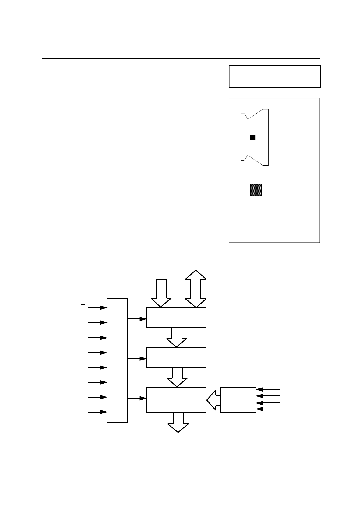
MC141511AMOTOROLA
LCD Segment Driver
CMOS
The MC141511A is an LCD frontplane (segment) driver chip which includes a 656 x 8 display RAM. The MC68HC05L10 microcomputer is the
companion device which provides the backplane drive.
The MC68HC05L10, together with one MC141511A, may be used to
drive a 5248-pixel muxed-by-41 display or a 4096-pixel muxed-by-32 display. Larger displays may be driven by adding additional MC141511A.
The MC141511A is a low operating voltage version of MC141511. It is
pin to pin compatible to the MC141511.
See Application Note AN-HK-13A.
• Operating Supply Voltage Range -
Control Logic, RAM, and Latch (VDD Pin): 2.7V to 5.5V
Frontplane Drivers (VLCD Pin): 4.5V to 13.2V
• Operating Temperature Range: -20 to 70˚C
• Direct Interface with the MC68HC05L10
• 656 x 8 Static RAM (Display RAM)
• 128 LCD Segment (Frontplane) Driving Signals
• 10-Bit Address Bus and 8-Bit Bidirectional Data Bus
• Selectable 1:32 or 1:41 Multiplex Ratios
• Available in Two Forms:
TAB (Tape Automated Bonding), 161 Contacts, 10 sprocket hole device
Die Form Without Gold Bumps, 159 Pads with 4.5 mil Pads Pitch
Control Logic
Display RAM
LCD D ATALATCH
SEGMENT DRIVER
A0-A9
D0-D7
V
LCD
V
SEGH
V
SEGL
V
SS
R/W
BPCLK
CE
LRS
PHI2
BPSYNC
DRIVER OUTP UTS
MS
VDD
LEVEL
SELECTOR
BLOCK DIAGRAM
MC141511A
MC141511AT2
TAB
MCC141511A
DIE
ORDERING INFORMATION
MCC141511A BARE DIE
MC141511AT2 TAB
MOTOROLA
SEMICONDUCTOR TECHNICAL DATA
REV 3
10/96
Page 2
MOTOROLA
3–20
MC141511A
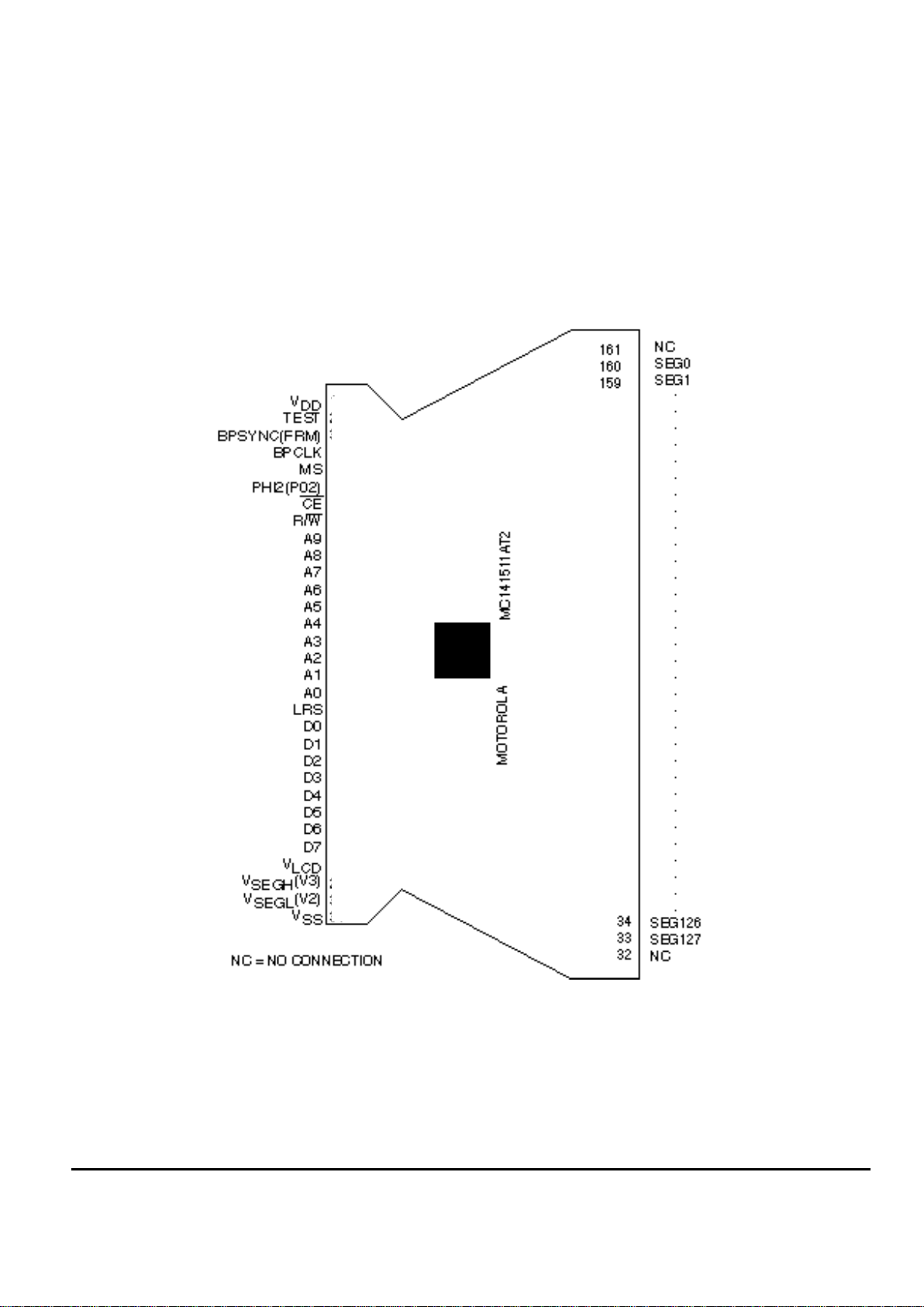
Figure 1A. TAB Package Contact Assignment (Copper View)
1
2
3
4
5
6
7
8
9
10
11
12
13
14
15
16
17
18
19
20
21
22
23
24
25
26
27
28
29
30
31
Page 3
3–21
MC141511AMOTOROLA
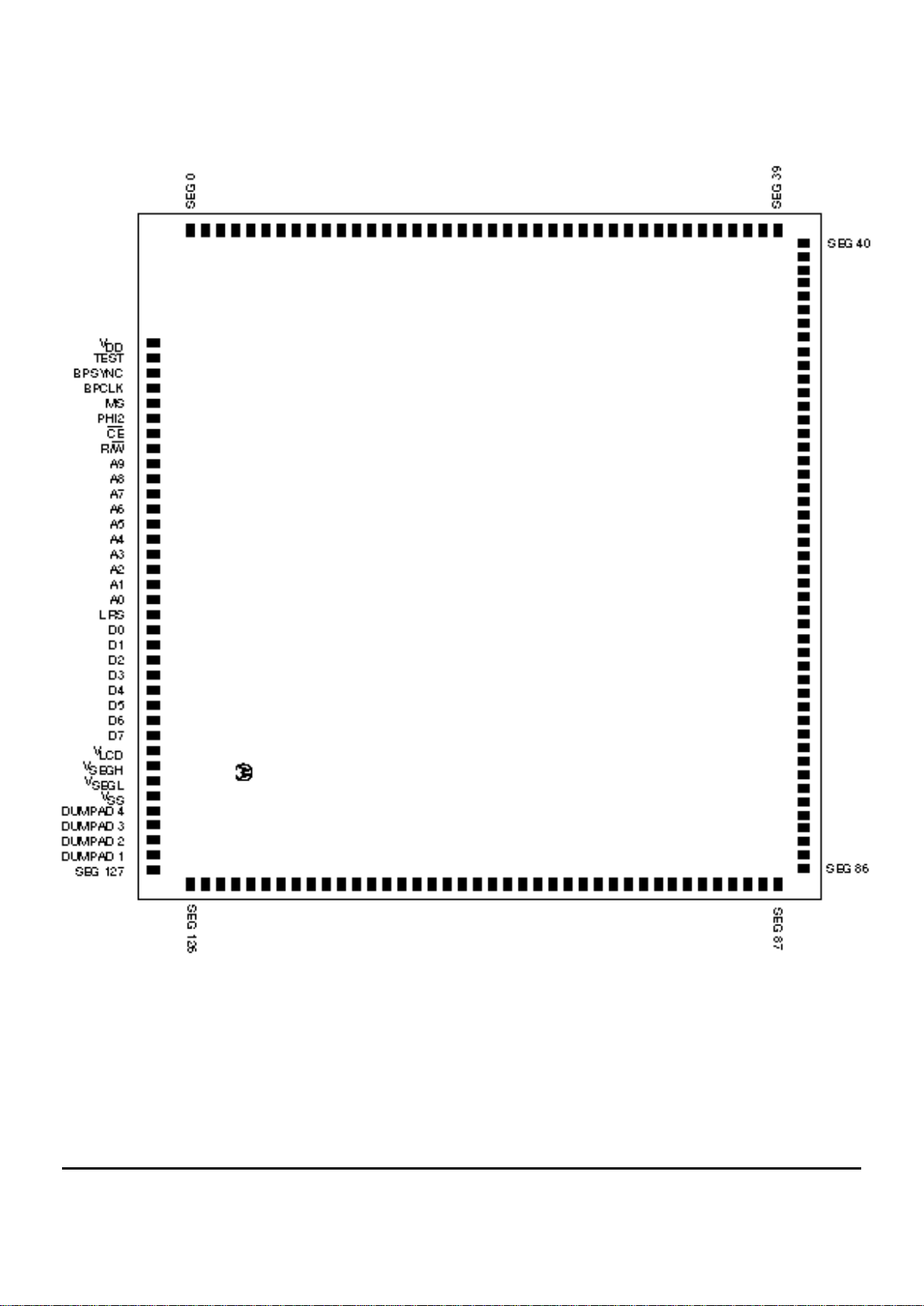
Figure 1B. Chip Pad Assignment
Page 4
MOTOROLA
3–22
MC141511A
Symbol Parameter Value Unit
V
DD
Supply Voltage -0.3 to +7.0 V
V
LCD
-0.3 to +14.0 V
V
in
Input Voltage VSS-0.3 to VDD+0.3 V
I Current Drain Per Pin Excluding VDD and V
SS
25 mA
T
A
Operating Temperature -20 to +70 ˚C
T
stg
Storage Temperature Range -65 to +150 ˚C
MAXIMUM RATINGS*(Voltages Referenced to VSS, TA = 25˚C)
* Maximum Ratings are those values beyond which damage to the device may occur. Functional
operation should be restricted to the limits in the Electrical Characteristics tables or Pin Description
section.
Symbol Parameter Min Typ Max Unit
V
DD
V
LCD
Operating Voltage
Supply Voltage
LCD Voltage
2.7
4.5
-
-
5.5
13.2
V
V
I
AC
I
DP
I
SB
I
AC
I
DP
I
SB
Supply Current
at VDD=5.5V (PHI2=3.685MHz)
ACCESS
DISPLAY
STANDBY (Using DON bit of the MCU)
at VDD=3.0V (PHI2=1.25MHz)
ACCESS
DISPLAY
STANDBY (Using DON bit of the MCU)
-
-
-
-
-
-
25
15
17
10
200
30
20
200
30
20
uA
uA
uA
uA
uA
uA
I
LCD
Supply Current at V
LCD
- - 200 uA
V
OL
V
OH
Output Voltage, Iload10.0uA -
V
LCD
-0.1
-
-
0.1
-
V
V
V
OH
Output High Voltage (Iload=1.6mA) D7-D0 VDD-0.8 - - V
V
OL
Output Low Voltage (Iload=1.6mA) D7-D0 - - 0.4 V
V
IH
Input High Voltage R/W, BPCLK, BPSYNC, PHI2, MS, CE, D7-D0 0.8xV
DD
-VDDV
V
IL
Input Low Voltage R/W, BPCLK, BPSYNC, PHI2, MS, CE, D7-D0 V
SS
- 0.2xV
DD
V
V
R
Data Retention 2.0 - - V
I
in
Input Current BPCLK, BPSYNC, R/W, PHI2, D7-D0 - - 1 uA
C
in
Capacitance R/W, BPCLK, BPSYNC, PHI2, MS, CE, D7-D0 - - 8 pF
I
OH
I
OL
Output current (VOH=4.5V, VOL=0.5V) D7-D0 +20
-
-
-
-
-20
uA
uA
ELECTRICAL CHARACTERISTICS (Voltage Referenced to VSS, TA= 25˚C)
This device contains circuitry to protect the inputs
against damage due to high static voltages or electric fields; however, it is advised that normal precautions to be taken to avoid application of any voltage
higher than maximum rated voltages to this high
impedance circuit. For proper operation it is recommended that Vin and V
out
be constrained to the
range VSS < or = (Vin or V
out
) < or = VDD. Reliability
of operation is enhanced if unused input are connected to an appropriate logic voltage level (e.g.,
either VSS or VDD). Unused outputs must be left
open. This device may be light sensitive. Caution
should be taken to avoid exposure of this device to
any light source during normal operation. This
device is not radiation protected.
Page 5
3–23
MC141511AMOTOROLA
AC ELECTRICAL CHARACTERISTICS - WRITE CYCLE (VDD=3.0V
10±
%, V
SS
=0V)
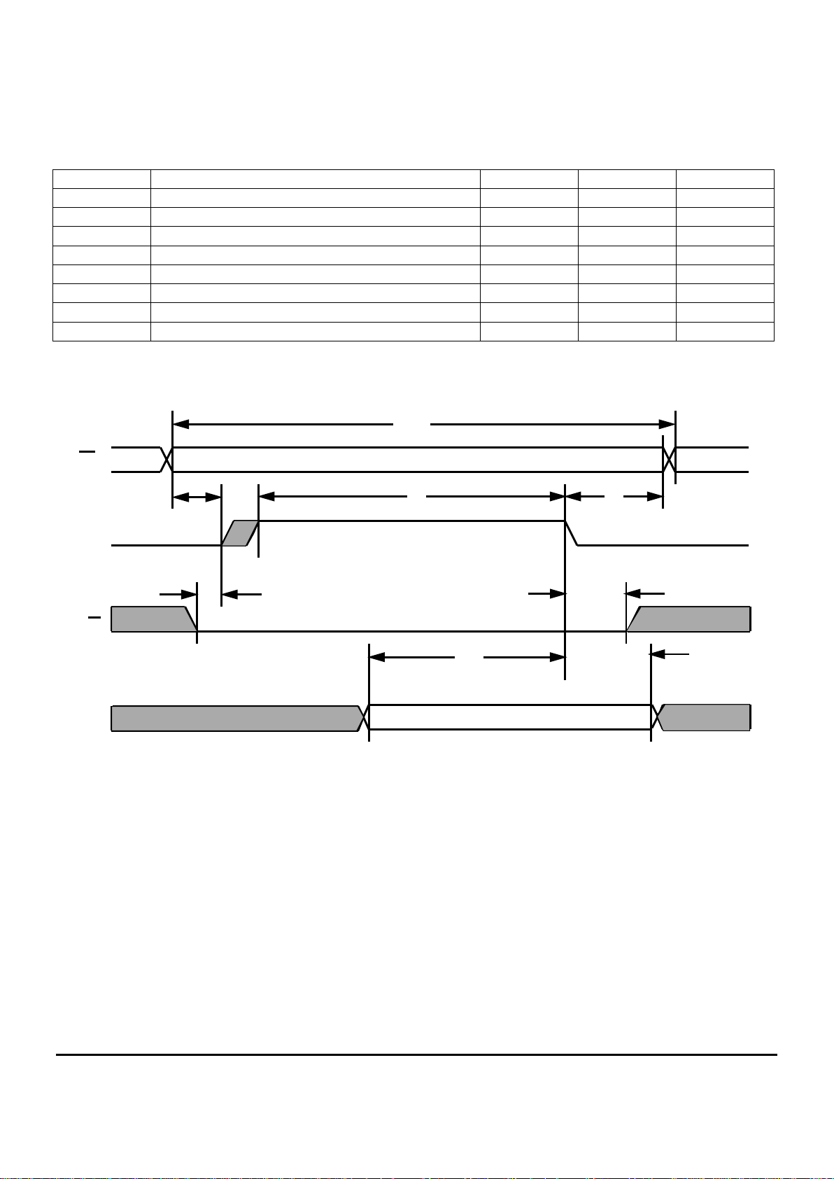
Symbol Parameter Min Max Unit
t
CYCW
Write Cycle Time 400 - ns
t
AS
Address Set Up Time 100 - ns
t
AH
Address Hold Time 70 - ns
t
CS
Chip Select Pulse Width 260 - ns
t
WCS
Write to Chip Select Delay Time 100 - ns
t
DSW
Data Setup Time 200 - ns
t
H
Input Hold Time 15 - ns
t
WH
Write Hold Time from Chip Select 70 - ns
Figure 2. Write Cycle Timing
CE
PHI2
R/W
D0-7
t
CYCW
t
AS
t
CS
t
AH
t
WH
t
WCS
t
DSW
t
H
Data in Stable
Page 6
MOTOROLA
3–24
MC141511A
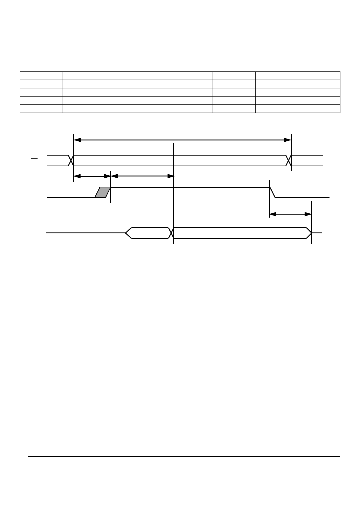
AC ELECTRICAL CHARACTERISTICS - READ CYCLE (VDD=3.0V
10±
%, V
SS
=0V)
Symbol Parameter Min Max Unit
t
CYCR
READ Cycle Time 400 - ns
t
AS
Address Setup Time 100 - ns
t
DDR
Data Delay Time (Read) - 350 ns
t
H
Output Hold Time 10 - ns
Figure 3. Read Cycle Timing
CE
PHI2
t
CYCR
t
DDR
D0-7
Data Valid
t
AS
t
H
Page 7

3–25
MC141511AMOTOROLA
VDD AND V
SS
The main dc power is supplied to the part by these two connections. VDD is the most-positive supply level for logic circuitry and VSS is
ground.
V
LCD
This supply connection provides the voltage level for the segment
drivers and is connected to the Vout connection of the MC68HC05L10
MCU.
V
SEGL
, V
SEGH
These inputs are connected to V2 and V3 of an external voltage
divider. See Figure 4.
D0 - D7
These connections form an eight bit wide bidirectional data bus
which are connected to D0 through D7 of the MC68HC05L10.
A0 - A9
These inputs form a ten-bit wide address bus for addressing the
display RAM and are connected to A0 through A9 of the
MC68HC05L10.
BPSYNC
This input is a periodic active-low signal from the MC68HC05L10
for timing synchronization. BPSYNC is connected to FRM of
MC68HC05L10. See Figure 5.
BPCLK
This input may be run as high as 4.096 kHz (50% duty cycle). It
provides the required frame frequency for the segment driver. It is connected to BPCLK of the MC68HC05L10. Thus, the frequency is usually
2.048 kHz. See Figure 5.
PHI2
This input is a bus clock input that is used for data bus timing synchronization. It is connected to P02 of MC68HC05L10.
SEG0 - SEG127
These 128 output lines provide the frontplane drive signals to the
LCD panel. These outputs are forced to a low level while display is
turned off. Any unused segment outputs should be left open.
CE
This is an active low chip enable input and is connected to either
CS1, CS2, CS3 or CS4 of the MC68HC05L10.
LRS
The left-right selection input defines the direction of the segment
driver display. See Figure 8.
0 or Low = SEG 0 - 127
1 or High = SEG 127 - 0
MS
This input selects how display RAM is addressed. Either a 1:32 or
1:41 multiplex ratio is possible.
0 or Low = 1:32 multiplex addressing
1 or High = 1:41 multiplex addressing
R/W
This input indicates which direction the data is to be passed over
the data bus. When R/W is low , the LCD driv er reads data from the data
bus (D0-D7). When R/W is high, the LCD driver writes data to the data
bus (D0-D7). This input is connected to R/W of MC68HC05L10.
TEST
Allowing this connection to float or connecting it to VSS (GND)
places the part in the normal mode of operation. This input has an onchip pulldown resistance of approximately 1M.
PIN DESCRIPTIONS
Figure 4. External Voltage Divider
V3
V2
Page 8

MOTOROLA
3–26
MC141511A
Figure 5. Relationship between BPSYNC and BPCLK
Figure 6. Display RAM Configuration
LRS = 1
LRS = 0
80
00
01 02 03
81
7E
FF
101 103102100 17F
180
1FF
181 182 183
1FE
17E
FE
7F
A BYTE
b0
b7
82 83
201 203202200 27F27E
280
28F
204 205 206 207
b0 b7
SEG0
SEG1
SEG2
SEG3
SEG127
SEG126
SEG125
SEG124
SEG126
SEG127
SEG1
SEG0
Page 9

3–27
MC141511AMOTOROLA
OPERATION OF LCD DRIVER
INTRODUCTION
The MC141511 is LCD driver with selectable 1: 32 or 1: 41 multiplex ratios. The device consists of the following functional blocks as
shown in the Block Diagram.
CONTROL LOGIC - accepts the control signals from the MCU and
generates internal signals for synchronisation.
DISPLAY RAM - stores the display data. Each bit of the display
RAM has one-to-one correspondence to a pixel of the LCD. The display
RAM is in vertical byte oriented format as shown in Figure 6 and the
way the display RAM is addressed depends on the multiplexing mode of
the LCD (Figure 8). With reference to Figure 6, the display RAM also
contains 16 bytes of memory which is in horizontal format ($280-$28F).
The display RAM is addressed when backplane reaches 41.
LEVEL SELECTOR - consists of a switching circuit to select
appropriate voltage levels from an e xternal voltage divider. See figure 4.
SEGMENT DRIVERS - provides the segment driving signals to the
LCD frontplane. See Figure 7.
The LCD driver clock is derived from the 2.048KHz BPCLK
and frame frequency is 64 Hz for 1:32 multiplex and 50 Hz for 1:41
multiplex ratio. See Figure 5.
GENERATION OF LCD BIAS LEVELS
Refer to Figure 4. In order to obtain optimum contrast for LCD
panels, the bias levels should be selected such that
BIAS = R/(4R+R1) = 1/(
MUX + 1)
V1/VLCD = 1/( MUX + 1)
V2/VLCD = 2/( MUX + 1)
V3/VLCD = ( MUX - 1)/( MUX + 1)
V4/VLCD = MUX /( MUX + 1)
Example: Mux = 41 ----- Bias = 1: 7.4,
R = 10K, R1 = 33K, VR = 100K
Mux = 32 ----- Bias = 1: 6.6,
R = 10K, R1 = 27K, VR = 100K
Page 10

MOTOROLA
3–28
MC141511A
1 2 3 4 N 1 2 3 4 N 1 2
COM (1)
COM (2)
SEG (X)
SEG (X)- COM (1)
SEG (X)- COM (2)
1 FRAME
GND
V1
V2
V3
V4
V
LCD
V1
V2
V3
V4
V1
V2
V3
V4
V1
V2
V3
V4
-V4
-V3
-V2
-V1
V1
V2
V3
V4
-V4
-V3
-V2
-V1
N = 32, 41
BPSYNC
(SIGNAL
FROM MCU,
FRM PIN)
GND
V
LCD
GND
V
LCD
GND
V
LCD
-V
LCD
GND
V
LCD
-V
LCD
Figure. 7 Driving Waveform of 1:5 Bias, 1:32 or 1:41 Multiplex Ratio
2 FRAMES = 1/32 OR 1/25 SEC
Page 11

3–29
MC141511AMOTOROLA
ONE SLAVE
$200 - $27F
$280 - $2FF
$300 - $37F
$380 - $3FF
1 : 32
$400 - $47F
$480 - $4FF
$500 - $57F
$580 - $5FF
$480 - $4FF
$500 - $57F
$580 - $5FF
$600 - $67F
1 : 41
$680 - $6FF
TWO SLAVES
THREE SLAVES
$200 - $27F
$280 - $2FF
$300 - $37F
$380 - $3FF
$400 - $47F
$200 - $27F
$280 - $2FF
$300 - $37F
$380 - $3FF
1 : 32
$200 - $27F
$280 - $2FF
$300 - $37F
$380 - $3FF
1 : 41
$400 - $47F
$1C0 - $1CF
$1C0 - $1CF
$1D0 - $1DF
1 : 41
$700 - $77F
$780 - $7FF
$800 - $87F
$880 - $8FF
$900 - $97F
1 : 32
$600 - $67F
$680 - $6FF
$700 - $77F
$780 - $7FF
$200 - $27F
$280 - $2FF
$300 - $37F
$380 - $3FF
$400 - $47F
$480 - $4FF
$500 - $57F
$580 - $5FF
$480 - $4FF
$500 - $57F
$580 - $5FF
$600 - $67F
$680 - $6FF
$200 - $27F
$280 - $2FF
$300 - $37F
$380 - $3FF
$400 - $47F
$1C0 - $1CF $1D0 - $1DF $1E0 - $1EF
1 : 32
$800 - $87F
$880 - $8FF
$900 - $97F
$980 - $9FF
$600 - $67F
$680 - $6FF
$700 - $77F
$780 - $7FF
$200 - $27F
$280 - $2FF
$300 - $37F
$380 - $3FF
$400 - $47F
$480 - $4FF
$500 - $57F
$580 - $5FF
1 : 41
FOUR SLAVES
$980 - $9FF
$A00 - $A7F
$A80 - $AFF
$B00 - $B7F
$B80 - $BFF
$700 - $77F
$780 - $7FF
$800 - $87F
$880 - $8FF
$900 - $97F
$480 - $4FF
$500 - $57F
$580 - $5FF
$600 - $67F
$680 - $6FF
$200 - $27F
$280 - $2FF
$300 - $37F
$380 - $3FF
$400 - $47F
$1D0 - $1DF
$1E0 - $1EF $1F0 - $1FF
$1C0 - $1CF
Figure 8. Display RAM Mapping for 1:32 and 1:41 Multiplex Ratio
Page 12

MOTOROLA
3–30
MC141511A
PACKAGE DIMENSIONS
MC141511AT2
TAB PACKAGE DIMENSION
(DO NOT SCALE THIS DRAWING)
Reference: 98ASL00183A Issue “A” released on 04/15/96
COPPER
POLYIMIDE
Page 13

3–31
MC141511AMOTOROLA
MC141511AT2
TAB PACKAGE DIMENSION
(DO NOT SCALE THIS DRAWING)
Reference: 98ASL00183A Issue “A” released on 04/15/96
Page 14

MOTOROLA
3–32
MC141511A
NOTES:
1. Dimensioning and tolerancing per ANSI Y14.5M, 1982.
2. Controlling dimension: millimeter
3. Copper thickness: 1 oz
MC141511AT2 TAB PACKAGE DIMENSION
Millimeters Inches Millimeters Inches
Dim Min Max Min Max Dim Min Max Min Max
A 46.55 47.55 1.8327 1.8720 AE 21.25 21.35 0.8366 0.8406
B 34.775 35.175 1.3691 1.3848 AF 1.95 2.05 0.0768 0.0807
C 28.947 29.007 1.1396 1.1420 AG 0.85 0.95 0.0335 0.0374
D 4.72 4.78 0.1858 0.1882 AH 0.85 0.95 0.0335 0.0374
E 1.951 2.011 0.0768 0.0792 AJ 9.75 9.85 0.3839 0.3878
F 1.951 2.011 0.0768 0.0792 AK 6.85 6.95 0.2697 0.2736
G 1 2 0.0394 0.0787 AL 4.75 4.85 0.1870 0.1909
H - - - - AM 1.95 2.05 0.0768 0.0807
J 7.469 8.469 0.2941 0.3334 AN 1.95 2.05 0.0768 0.0807
K 9.04 10.04 0.3559 0.3953 AP 0.085 0.095 0.0033 0.0037
L 0.48 0.52 0.0189 0.0205 AR 0.35 0.45 0.0014 0.0177
M 1.26 1.28 0.0496 0.0504 AS 0.35 0.45 0.0014 0.0177
N 4.95 5.05 0.1949 0.1988 AT 0.6 0.7 0.0236 0.0276
P 20.45 20.55 0.8051 0.8091 AU 0.6 0.7 0.0236 0.0276
R 20.45 20.55 0.8051 0.8091 AV 0.75 0.85 0.0295 0.0335
S 9.78 9.88 0.3850 0.3890 AW 0.75 0.85 0.0295 0.0335
T 23.155 23.255 0.9116 0.9156 AX 1.75 1.85 0.0689 0.0728
U 23.155 23.255 0.9116 0.9156 AY 0.34 0.36 0.0134 0.0142
V 22.53 22.62 0.8870 0.8905 AZ 0.15 0.19 0.0059 0.0075
W 22.53 22.62 0.8870 0.8905 BA 13.7 14.3 0.5394 0.5630
X 23.1 23.2 0.9094 0.9134 BB 1.22 1.32 0.0480 0.0520
Y 23.1 23.2 0.9094 0.9134 BC 1.22 1.32 0.0480 0.0520
Z 19.95 20.05 0.7854 0.7894 BD 0.45 0.55 0.0177 0.0217
AA - 0.2 - 0.0079 BE 11.35 11.45 0.4469 0.4508
AB 0.686 0.838 0.027 0.033 BF 0.12 0.22 0.0047 0.0087
AC 0.068 0.063 0.0027 0.0024 BG 12.35 12.45 0.4862 0.4902
AD 0.579 0.629 0.0227 0.0247
Reference: 98ASL00183A Issue “A” released on 04/15/96
Page 15

3–33
MC141511AMOTOROLA
MC141511AT2
Reference: 98ASL00183A Issue “A” released on 04/15/96
Page 16

MOTOROLA
3–34
MC141511A
MCC141511A PAD COORDINATES
(UNIT: um)
Pin Pin Pin Pin
Name X Y Name X Y Name X Y Name X Y
VDD -1874.62 -2498.76 SEG126 2728.66 -2233.88 SEG86 2630.76 2432.32 SEG39 -2728.66 2227.72
TEST -1738.66 -2498.76 SEG125 2728.66 -2119.48 SEG85 2516.36 2432.32 SEG38 -2728.66 2113.32
BPSYNC -1611.06 -2498.76 SEG124 2728.66 -2005.08 SEG84 2401.96 2432.32 SEG37 -2728.66 1998.92
BPCLK -1483.46 -2498.76 SEG123 2728.66 -1890.68 SEG83 2287.56 2432.32 SEG36 -2728.66 1884.52
MS -1355.86 -2498.76 SEG122 2728.66 -1776.28 SEG82 2173.16 2432.32 SEG35 -2728.66 1770.12
PHI2 -1228.26 -2498.76 SEG121 2728.66 -1661.88 SEG81 2058.76 2432.32 SEG34 -2728.66 1655.72
CE -1100.66 -2498.76 SEG120 2728.66 -1547.48 SEG80 1944.36 2432.32 SEG33 -2728.66 1541.32
RW -973.06 -2498.76 SEG119 2728.66 -1433.08 SEG79 1829.96 2432.32 SEG32 -2728.66 1426.92
A9 -845.46 -2498.76 SEG118 2728.66 -1318.68 SEG78 1715.56 2432.32 SEG31 -2728.66 1312.52
A8 -717.86 -2498.76 SEG117 2728.66 -1204.28 SEG77 1601.16 2432.32 SEG30 -2728.66 1198.12
A7 -590.26 -2498.76 SEG116 2728.66 -1089.88 SEG76 1486.76 2432.32 SEG29 -2728.66 1083.72
A6 -462.66 -2498.76 SEG115 2728.66 -975.48 SEG75 1372.36 2432.32 SEG28 -2728.66 969.32
A5 -335.06 -2498.76 SEG114 2728.66 -861.08 SEG74 1257.96 2432.32 SEG27 -2728.66 854.92
A4 -207.46 -2498.76 SEG113 2728.66 -746.68 SEG73 1143.56 2432.32 SEG26 -2728.66 740.52
A3 -79.86 -2498.76 SEG112 2728.66 -632.28 SEG72 1029.16 2432.32 SEG25 -2728.66 626.12
A2 47.74 -2498.76 SEG111 2728.66 -517.88 SEG71 914.76 2432.32 SEG24 -2728.66 511.72
A1 175.34 -2498.76 SEG110 2728.66 -403.48 SEG70 800.36 2432.32 SEG23 -2728.66 397.32
A0 302.94 -2498.76 SEG109 2728.66 -289.08 SEG69 685.96 2432.32 SEG22 -2728.66 282.92
LRS 430.54 -2498.76 SEG108 2728.66 -174.68 SEG68 571.56 2432.32 SEG21 -2728.66 168.52
D0 558.14 -2498.76 SEG107 2728.66 -60.28 SEG67 457.16 2432.32 SEG20 -2728.66 54.12
D1 685.74 -2498.76 SEG106 2728.66 54.12 SEG66 342.76 2432.32 SEG19 -2728.66 -60.28
D2 813.34 -2498.76 SEG105 2728.66 168.52 SEG65 228.36 2432.32 SEG18 -2728.66 -174.68
D3 940.94 -2498.76 SEG104 2728.66 282.92 SEG64 113.96 2432.32 SEG17 -2728.66 -289.08
D4 1068.54 -2498.76 SEG103 2728.66 397.32 SEG63 -0.44 2432.32 SEG16 -2728.66 -403.48
D5 1196.14 -2498.76 SEG102 2728.66 511.72 SEG62 -114.84 2432.32 SEG15 -2728.66 -517.88
D6 1323.74 -2498.76 SEG101 2728.66 626.12 SEG61 -229.24 2432.32 SEG14 -2728.66 -632.28
D7 1451.12 -2498.76 SEG100 2728.66 740.52 SEG60 -343.64 2432.32 SEG13 -2728.66 -746.68
VLCD 1578.94 -2498.76 SEG99 2728.66 854.92 SEG59 -458.04 2432.32 SEG12 -2728.66 -861.08
VSEGH 1706.54 -2498.76 SEG98 2728.66 969.32 SEG58 -572.44 2432.32 SEG11 -2728.66 -975.48
VSEGL 1834.14 -2498.76 SEG97 2728.66 1083.72 SEG57 -686.84 2432.32 SEG10 -2728.66 -1089.88
VSS 1979.78 -2498.76 SEG96 2728.66 1198.12 SEG56 -801.24 2432.32 SEG9 -2728.66 -1204.28
DUMPAD 4 2111.78 -2498.76 SEG95 2728.66 1312.52 SEG55 -915.64 2432.32 SEG8 -2728.66 -1318.68
DUMPAD 3 2239.38 -2498.76 SEG94 2728.66 1426.92 SEG54 -1030.04 2432.32 SEG7 -2728.66 -1433.08
DUMPAD 2 2366.98 -2498.76 SEG93 2728.66 1541.32 SEG53 -1144.44 2432.32 SEG6 -2728.66 -1547.48
DUMPAD 1 2494.58 -2498.76 SEG92 2728.66 1655.72 SEG52 -1258.84 2432.32 SEG5 -2728.66 -1661.88
SEG127 2619.54 -2498.76 SEG91 2728.66 1770.12 SEG51 -1373.24 2432.32 SEG4 -2728.66 -1776.28
SEG90 2728.66 1884.52 SEG50 -1487.64 2432.32 SEG3 -2728.66 -1890.68
SEG89 2728.66 1998.92 SEG49 -1602.04 2432.32 SEG2 -2728.66 -2005.08
SEG88 2728.66 2113.32 SEG48 -1716.44 2432.32 SEG1 -2728.66 -2119.48
SEG87 2728.66 2227.72 SEG47 -1830.84 2432.32 SEG0 -2728.66 -2233.88
SEG46 -1945.24 2432.32
SEG45 -2059.64 2432.32
SEG44 -2174.04 2432.32
SEG43 -2288.44 2432.32
SEG42 -2402.84 2432.32
SEG41 -2517.24 2432.32
SEG40 -2631.64 2432.32
Die Size : 240.0 x 212.0 mil
2
Pad Pitch : 4.5 mil
Note : 1 mil ~ 25.4 m
DUMPAD 1-4: Dummy pad without connections to internal circuitry
Page 17

3–35
MC141511AMOTOROLA
10K
10K
30K
10K
10K
TYPICAL APPLICATIONS
128 X 41 SINGLE PANEL LCD SYSTEM WITH MC68HC05L10
41 X 128 dots LCD Panel
SEG0-SEG127
BP0-BP40
MC68HC05L10
BP0-BP40
MC141511A
SEG0-SEG127
BPCLK
FRM
CS1
R/
W
PO2
A0-A9 D0-D7
VLCD
VSEGH
VSEGL
BPCLK
BPSYNC
CE
MS
LRS
R/
W
PHI2
VDD
VSS
VLCD
VOUT
V4
V1
Trimmer for
Contrast
Control
LCD
POWER
SUPPLY
V4
V3
V2
V1
A0-A9D0-D7
VDD
VSS
10
8
Note : Full capability of MC68HC05L10 can control up to four MC141511A slave LCD drivers with 41 x 512 dots LCD panel.
Refer to application note, MC68HC05L10 AN ENHANCED VERSION OF L9 FOR HANDHELD EQUIPMENT APPLI-
CATIONS (AN-HK-13A) for more details.
+5V +5V
+5V
 Loading...