

Page 1
Order this document by MC1404/D
The MC1404 of ICs is a family of temperature–compensated voltage
references for precision data conversion applications, such as A/D, D/A, V/F ,
and F/V. Advances in laser–trimming and ion–implanted devices, as well as
monolithic fabrication techniques, make these devices stable and accurate
to 12 bits over both military and commercial temperature ranges. In addition
to excellent temperature stability, these parts offer excellent long–term
stability and low noise.
• Output Voltages: Standard, 5.0 V, 6.25 V, 10 V
• Trimmable Output: > ± 6%
• Wide Input Voltage Range: V
+ 2.5 V to 40 V
ref
• Low Quiescent Current: 1.25 mA Typical
• Temperature Coefficient: 10 ppm/°C Typical
• Low Output Noise: 12 µV p–p Typical
• Excellent Ripple Rejection: > 80 dB Typical
T ypical Applications
• Voltage Reference for 8 to 12 Bit D/A Converters
• Low T
Zener Replacement
C
• High Stability Current Reference
• MPU D/A and A/D Applications
PRECISION LOW DRIFT
VOLTAGE REFERENCES
5.0, 6.25, and 10–VOLT OUTPUT VOLTAGES
SEMICONDUCTOR
TECHNICAL DATA
8
1
P SUFFIX
PLASTIC PACKAGE
CASE 626
Figure 1. Voltage Output 8–Bit DAC Using MC1404P10
+ 5.0
5.0 k
In
5.0 k
0.05
2
3
Digital
Inputs
MSB
LSB
Ref
8 Bit
DAC
Out
– 15
MOTOROLA ANALOG IC DEVICE DATA
75 pF
5.0 k
7
–
LF156A
+
4
6
+ 15
1
– 15
+ 15
2
MC1404P10
4
5
+ 10 V
0 to
PIN CONNECTIONS
V
TEMP
NC
V
in
Gnd
1
2
3
4
7
6
5
NC8
NC
V
out
TRIM
ORDERING INFORMATION
Operating
Device
MC1404P5
MC1404P6 TA = 0° to +70°C
MC1404P10 Plastic DIP
Motorola, Inc. 1996 Rev 2
Temperature Range
Package
Plastic DIP
Plastic DIP
1
Page 2
MAXIMUM RATINGS
Rating Symbol Value Unit
Input Voltage V
Storage Temperature T
Junction Temperature T
Operating Ambient Temperature Range T
stg
MC1404
in
J
A
40 V
– 65 to + 150 °C
+ 175 °C
0 to + 70 °C
ELECTRICAL CHARACTERISTICS (V
Characteristic
Output Voltage V
(IO = 0 mA) MC1404P5
Output Voltage Tolerance – – ± 0.1 ± 1.0 %
Output Trim Range (Figure 10) ∆V
(RP = 100 kΩ)
Output Voltage Temperature Coefficient, ∆VO/∆T – 10 40 ppm/°C
Over Full Temperature Range
Maximum Output Voltage Change ∆V
Over Temperature Range MC1404P5
Line Regulation (Note 1) Reg
(Vin = V
Load Regulation (Note 1) Reg
(0 p IO p 10 mA)
Quiescent Current I
(IO = 0 mA)
Short Circuit Current I
Long Term Stability – – 25 – ppm/1000 hrs
NOTE: 1. Includes thermal effects.
+ 2.5 V to 40 V, I
out
= 0 mA)
out
= 15 V, TA = 25°C, and Trim Terminal not connected, unless otherwise noted.)
in
Symbol Min Typ Max Unit
O
MC1404P6
MC1404P10
TRIM
O
MC1404P6
MC1404P10
line
load
Q
sc
4.95
6.19
9.9
± 6.0 – – %
–
–
–
– 2.0 6.0 mV
– – 10 mV
– 1.2 1.5 mA
– 20 45 mA
5.0
6.25
10
–
–
–
5.05
6.31
10.1
14
17.5
28
V
mV
DYNAMIC CHARACTERISTICS (V
Characteristic Symbol Min Typ Max Unit
Turn–On Settling Time t
(to ± 0.01%)
Output Noise Voltage – P to P V
(Bandwidth 0.1 to 10 Hz)
Small–Signal Output Impedance r
120 Hz
500 Hz
Power Supply Rejection Ratio PSRR 70 80 – dB
= 15 V, TA = 25°C, all voltage ranges, unless otherwise noted.)
in
S
n
o
– 50 – µs
– 12 – µV
–
–
0.15
0.2
–
–
Ω
2
MOTOROLA ANALOG IC DEVICE DATA
Page 3
MC1404
TYPICAL CHARACTERISTICS
V
TEMP
, OUTPUT VOL TAGE (V)
out
V
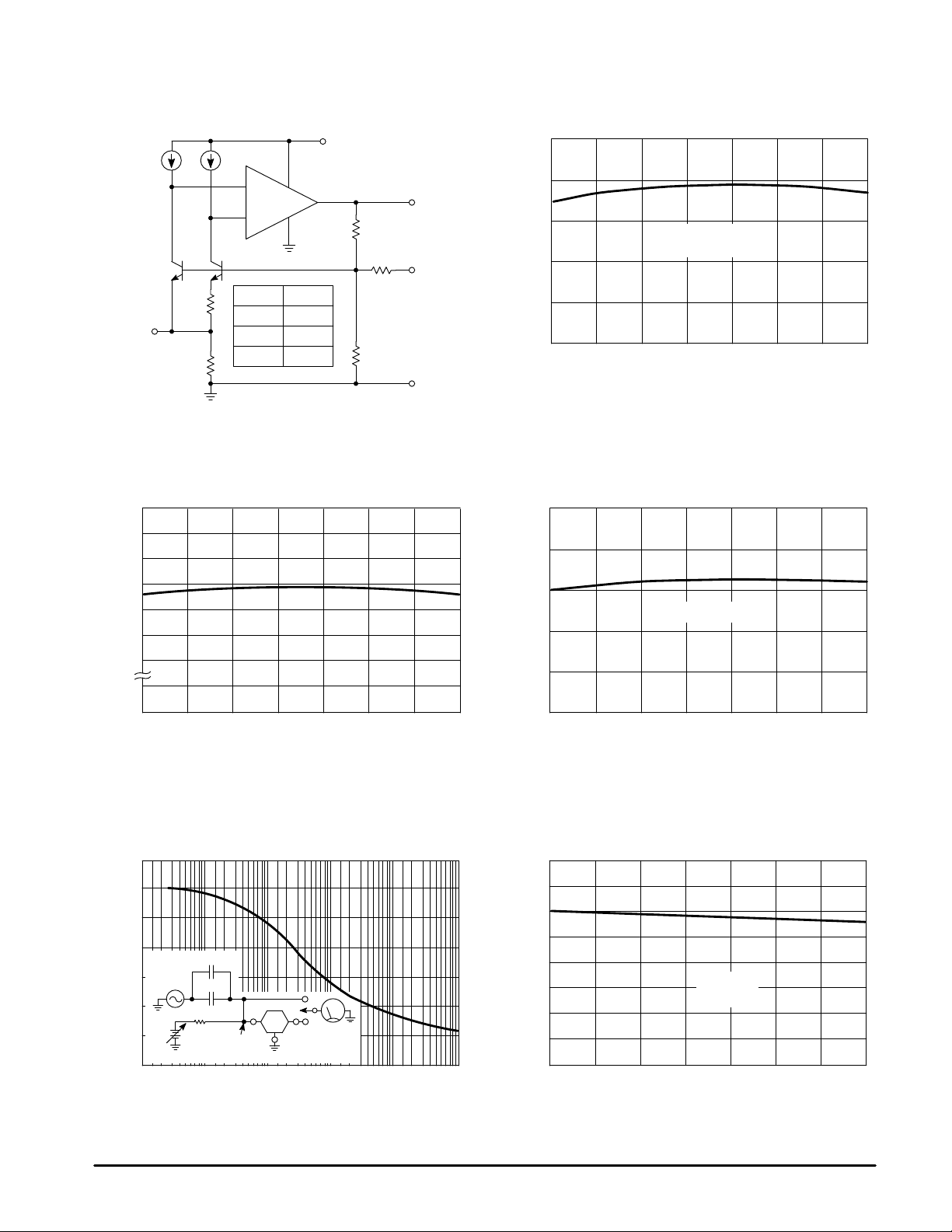
Figure 2. Simplified Device Diagram
V
in
2
–
+
R
3.75 k
3
5.0 k
8.75 k
V
o
5.0 V
6.25 V
10 V
Figure 4. Output V oltage versus Temperature
MC1404P10
10.04
10.02
10.00
9.98
9.96
9.94
R
5.0 k
1.25 k
6
5
4
V
out
TRIM
Figure 3. Line Regulation versus T emperature
2.5
2.0
1.5
Vin = V
+2.5 V to 40 V
ref
I
= 0 mA
1.0
out
, LINE REGULATION (mV)
out
V
0.5
∆
0
10 6020
T
A
30
, AMBIENT TEMPERATURE (
Figure 5. Load Regulation versus T emperature
0.010
0.008
0.006
Load Change 0 to 10 mA
0.004
LOAD REGULATION (%/mA)
0.002
50 70040
°
C)
0
01020304050 60
TA, AMBIENT TEMPERATURE (
°
C)
Figure 6. Power Supply Rejection Ratio
versus Frequency
90
80
70
60
HP209A
50
3.0 Vrms
40
30
20
PSRR, POWER SUPPLY REJECTION RATIO (dB)
0.01 0.1 1001.0
0.1
µ
F
500
µ
F
+
–
1.0 k
+
21.3 V
–
2
Set Node to
20 V Average
DUT
6
HP3400A
4
10 1000
f, FREQUENCY (kHz)
70
0
10 6020 50 7004030
TA, AMBIENT TEMPERATURE (
°
C)
Figure 7. Quiescent Current versus T emperature
1.6
1.4
1.2
1.0
0.8
Vin = 15 V
I
= 0 mA
out
°
C)
, QUIESCENT CURRENT (mA)
Q
I
0.6
0.4
0.2
0
10 6020 50 7004030
TA, AMBIENT TEMPERATURE (
MOTOROLA ANALOG IC DEVICE DATA
3
Page 4

Figure 8. Short Circuit Current
versus T emperature
40
35
30
25
20
15
10
, SHORT CIRCUIT CURRENT (mA)
5.0
sc
I
0
10 6020 50 7004030
TA, AMBIENT TEMPERATURE (°C)
Vin = 15 V
Figure 10. Output Trim Configuration Figure 11. Precision Supply Using MC1404
+ 15 V
2
V
6
in
V
o
MC1404
The MC1404 trim terminal can be used to adjust the output voltage
over a ±6.0% range. For example, the output can be set to 10.000 V
or to 10.240 V for binary applications. For trimming, Bourns type
3059, 100 kΩ or 200 kΩ trimpot is recommended.
Although Figure 10 illustrates a wide trim range, temperature
coefficients may become unpredictable for trim > ±6.0%.
5
TRIM
Gnd
4
Output Adjustment
R
P
100 k
Output
MC1404
Figure 9. V
1.0
0.8
0.6
0.4
0.2
TEMP
V , TEMPERATURE OUTPUT (V)
0
The addition of a power transistor, a resistor, and a capacitor
converts the MC1404 into a precision supply with one ampere
current capability . At V+ = 15 V, the MC1404 can carry in excess of
14 mA of load current with good regulation. If the power transistor
current gain exceeds 75, a one ampere supply can be realized.
10 6020 50 7004030
330
2
V
in
MC1404
Gnd
4
Output versus Temperature
TEMP
I
V
TEMP
TA, AMBIENT TEMPERATURE (°C)
MPS–U51A
µ
F
0.01
6
V
o
Output Power Boosting
nA
= 10
V+
5.0, 6.25,
10 V @ 1/2 Amp
Figure 12. Ultra Stable Reference for MC1723 V oltage Regulator
Supply
2
MC1404P5
4
6
0.1
µ
F
3(5)
2(4)
4
8(12)
+
–
9(13)5(7)
0.001
7(11)
µ
F
10(2)
MC1723
6(10)
1(3)
R
sc
R
o
4.7 k
V
out
Ro)
4.7 k
V
out
I
omax
5.0 V
[
0.6 V
R
sc
ǒ
+
4.7 k
Ǔ
MOTOROLA ANALOG IC DEVICE DATA
Page 5

MC1404
Figure 13. 5.0 V, 6.0 Amp, 25 kHz Switching Regulator with Separate Ultra–Stable Reference
+ 10 to + 30 ln
+
–
2
6
MC1404P5
100 k
5
TRIM
(opt)
4
1000
50 V
0.01
Ceramic
2.2 k
+5.0 V Out
200 mA to
6.0 Amps
µ
F
µ
H
130
120
1N3889
Motorola
TL495CN
–
+
+
–
1410
+
–
17
18
1
2
3
µ
F
5000
6.8 V
(Low ESR)
220 k
0.001 µF
2.2 k
2N5879
µ
F
0.01 µF
50 V
Ceramic
12
Pulse Width
Modulator
Oscillator
5
µ
F
0.005
33
130
8
11
64
10 k
97
12.5 to
40 V
Input
Figure 14. Reference for a High Speed DAC
26
MC1404P10
4
10 V Reference
R1 and R2 values depend
on the current requirements
of the DAC.
R1 R2
µ
F
0.1
Digital
Inputs
Analog
Output
Ladder
and
Switches
High Speed DAC
MOTOROLA ANALOG IC DEVICE DATA
5
Page 6

NOTE 2
–T–
SEATING
PLANE
H
58
–B–
14
F
–A–
C
N
D
K
G
0.13 (0.005) B
M
T
MC1404
OUTLINE DIMENSIONS
P1 SUFFIX
PLASTIC PACKAGE
CASE 626–05
ISSUE K
L
J
M
M
A
M
NOTES:
1. DIMENSION L TO CENTER OF LEAD WHEN
FORMED PARALLEL.
2. PACKAGE CONTOUR OPTIONAL (ROUND OR
SQUARE CORNERS).
3. DIMENSIONING AND TOLERANCING PER ANSI
Y14.5M, 1982.
DIM MIN MAX MIN MAX
A 9.40 10.16 0.370 0.400
B 6.10 6.60 0.240 0.260
C 3.94 4.45 0.155 0.175
D 0.38 0.51 0.015 0.020
F 1.02 1.78 0.040 0.070
G 2.54 BSC 0.100 BSC
H 0.76 1.27 0.030 0.050
J 0.20 0.30 0.008 0.012
K 2.92 3.43 0.115 0.135
L 7.62 BSC 0.300 BSC
M ––– 10 ––– 10
N 0.76 1.01 0.030 0.040
INCHESMILLIMETERS
__
6
MOTOROLA ANALOG IC DEVICE DATA
Page 7

MC1404
NOTES
MOTOROLA ANALOG IC DEVICE DATA
7
Page 8

MC1404
Motorola reserves the right to make changes without further notice to any products herein. Motorola makes no warranty , representation or guarantee regarding
the suitability of its products for any particular purpose, nor does Motorola assume any liability arising out of the application or use of any product or circuit, and
specifically disclaims any and all liability, including without limitation consequential or incidental damages. “T ypical” parameters which may be provided in Motorola
data sheets and/or specifications can and do vary in different applications and actual performance may vary over time. All operating parameters, including “Typicals”
must be validated for each customer application by customer’s technical experts. Motorola does not convey any license under its patent rights nor the rights of
others. Motorola products are not designed, intended, or authorized for use as components in systems intended for surgical implant into the body, or other
applications intended to support or sustain life, or for any other application in which the failure of the Motorola product could create a situation where personal injury
or death may occur. Should Buyer purchase or use Motorola products for any such unintended or unauthorized application, Buyer shall indemnify and hold Motorola
and its officers, employees, subsidiaries, affiliates, and distributors harmless against all claims, costs, damages, and expenses, and reasonable attorney fees
arising out of, directly or indirectly, any claim of personal injury or death associated with such unintended or unauthorized use, even if such claim alleges that
Motorola was negligent regarding the design or manufacture of the part. Motorola and are registered trademarks of Motorola, Inc. Motorola, Inc. is an Equal
Opportunity/Affirmative Action Employer.
How to reach us:
USA/EUROPE/ Locations Not Listed: Motorola Literature Distribution; JAPAN: Nippon Motorola Ltd.; T atsumi–SPD–JLDC, 6F Seibu–Butsuryu–Center,
P.O. Box 20912; Phoenix, Arizona 85036. 1–800–441–2447 or 602–303–5454 3–14–2 Tatsumi Koto–Ku, Tokyo 135, Japan. 03–81–3521–8315
MFAX: RMF AX0@email.sps.mot.com – TOUCHT ONE 602–244–6609 ASIA/PACIFIC: Motorola Semiconductors H.K. Ltd.; 8B Tai Ping Industrial Park,
INTERNET: http://Design–NET.com 51 Ting Kok Road, Tai Po, N.T., Hong Kong. 852–26629298
8
◊
MOTOROLA ANALOG IC DEVICE DATA
MC1404/D
*MC1404/D*
 Loading...