

Page 1
MOTOROLA CMOS LOGIC DATA
1
MC14046B
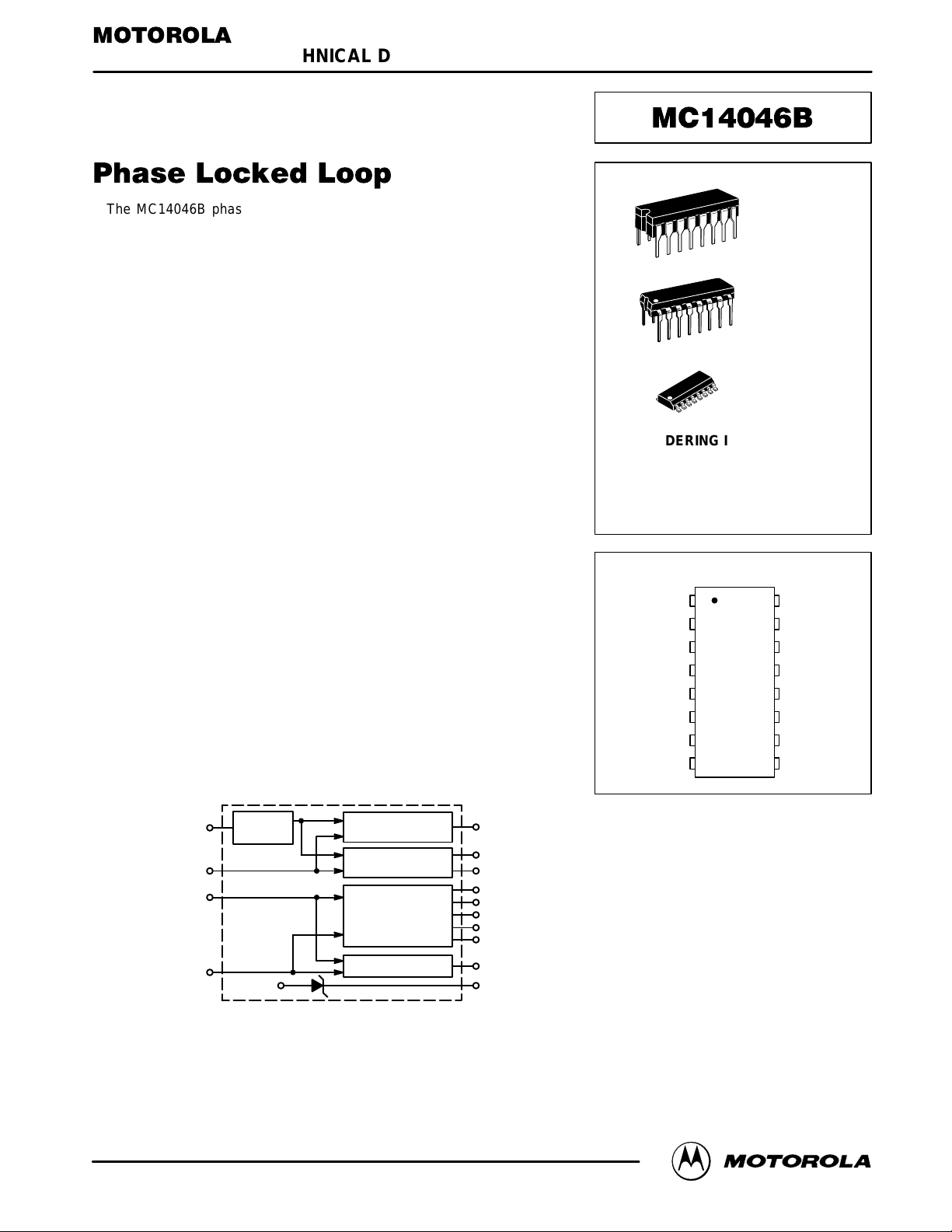
The MC14046B phase locked loop contains two phase comparators, a
voltage–controlled oscillator (VCO), source follower, and zener diode. The
comparators have two common signal inputs, PCAin and PCBin. Input PCA
in
can be used directly coupled to large voltage signals, or indirectly coupled
(with a series capacitor) to small voltage signals. The self–bias circuit
adjusts small voltage signals in the linear region of the amplifier. Phase
comparator 1 (an exclusive OR gate) provides a digital error signal PC1
out
,
and maintains 90° phase shift at the center frequency between PCAin and
PCBin signals (both at 50% duty cycle). Phase comparator 2 (with leading
edge sensing logic) provides digital error signals, PC2
out
and LD, and
maintains a 0° phase shift between PCAin and PCBin signals (duty cycle is
immaterial). The linear VCO produces an output signal VCO
out
whose
frequency is determined by the voltage of input VCOin and the capacitor and
resistors connected to pins C1A, C1B, R1, and R2. The source–follower
output SF
out
with an external resistor is used where the VCOin signal is
needed but no loading can be tolerated. The inhibit input Inh, when high,
disables t he VCO a nd s ource follower t o minimize s tandby p ower
consumption. The zener diode can be used to a ssist in p ower supply
regulation.
Applications include FM and F SK modulation and d emodulation, frequency synthesis and multiplication, frequency discrimination, tone decoding, d ata synchronization a nd conditioning, voltage–to–frequency
conversion and motor speed control.
• Buffered Outputs Compatible with MHTL and Low–Power TTL
• Diode Protection on All Inputs
• Supply Voltage Range = 3.0 to 18 V
• Pin–for–Pin Replacement for CD4046B
• Phase Comparator 1 is an Exclusive Or Gate and is Duty Cycle Limited
• Phase Comparator 2 switches on Rising Edges and is not Duty Cycle
Limited
BLOCK DIAGRAM
PCA
in
PCB
in
VCO
in
INH
14
3
9
5
VDD = PIN 16
VSS = PIN 8
2 PC1
out
13 PC2
out
1 LD
4 VCO
out
11 R1
12 R2
6 C1
A
7 C1
B
10 SF
out
15 ZENERV
SS
SELF BIAS
CIRCUIT
PHASE
COMPARATOR 1
PHASE
COMPARATOR 2
VOLTAGE
CONTROLLED
OSCILLATOR
(VCO)
SOURCE FOLLOWER
SEMICONDUCTOR TECHNICAL DATA
Motorola, Inc. 1995
REV 3
1/94
L SUFFIX
CERAMIC
CASE 620
ORDERING INFORMATION
MC14XXXBCP Plastic
MC14XXXBCL Ceramic
MC14XXXBDW SOIC
TA = – 55° to 125°C for all packages.
P SUFFIX
PLASTIC
CASE 648
DW SUFFIX
SOIC
CASE 751G
PIN ASSIGNMENT
13
14
15
16
9
10
11
125
4
3
2
1
8
7
6
R2
PC2
out
PCA
in
ZENER
V
DD
VCO
in
SF
out
R1
VCO
out
PCB
in
PC1
out
LD
V
SS
C1
B
C1
A
INH
Page 2
MOTOROLA CMOS LOGIC DATAMC14046B
2
MAXIMUM RATINGS* (Voltages Referenced to V
SS
)
Rating
Symbol
Value
Unit
DC Supply Voltage
V
DD
– 0.5 to + 18
Vdc
Input Voltage, All Inputs
V
in
– 0.5 to VDD + 0.5
Vdc
DC Input Current, per Pin
I
in
± 10
mAdc
Power Dissipation, per Package†
P
D
500
mW
Operating Temperature Range
T
A
– 55 to + 125
_
C
Storage Temperature Range
T
stg
– 65 to + 150
_
C
*Maximum Ratings are those values beyond which damage to the device may occur.
†Temperature Derating:
Plastic “P and D/DW” Packages: – 7.0 mW/_C From 65_C To 125_C
Ceramic “L” Packages: – 12 mW/_C From 100_C To 125_C
ELECTRICAL CHARACTERISTICS (Voltages Referenced to V
SS
)
V
DD
– 55_C
25_C
125_C
Characteristic
Symbol
V
DD
Vdc
Min
Max
Min
Typ
Max
Min
Max
Unit
“0” Level
Vin = VDD or 0
V
OL
5.0
10
15
—
—
—
0.05
0.05
0.05
—
—
—
0
0
0
0.05
0.05
0.05
—
—
—
0.05
0.05
0.05
Vdc
“1” Level
Vin = 0 or V
DD
V
OH
5.0
10
15
4.95
9.95
14.95
—
—
—
4.95
9.95
14.95
5.0
10
15
—
—
—
4.95
9.95
14.95
—
—
—
Vdc
“0” Level
(VO = 4.5 or 0.5 Vdc)
(VO = 9.0 or 1.0 Vdc)
(VO = 13.5 or 1.5 Vdc)
V
IL
5.0
10
15
—
—
—
1.5
3.0
4.0
—
—
—
2.25
4.50
6.75
1.5
3.0
4.0
—
—
—
1.5
3.0
4.0
Vdc
“1” Level
(VO = 1.0 or 9.0 Vdc)
(VO = 1.5 or 13.5 Vdc)
V
IH
5.0
10
15
3.5
7.0
11
—
—
—
3.5
7.0
11
2.75
5.50
8.25
—
—
—
3.5
7.0
11
—
—
—
Vdc
I
OH
5.0
5.0
10
15
– 1.2
– 0.25
– 0.62
– 1.8
—
—
—
—
– 1.0
– 0.2
– 0.5
– 1.5
– 1.7
– 0.36
– 0.9
– 3.5
—
—
—
—
– 0.7
– 0.14
– 0.35
– 1.1
—
—
—
—
mAdc
I
OL
5.0
10
15
0.64
1.6
4.2
—
—
—
0.51
1.3
3.4
0.88
2.25
8.8
—
—
—
0.36
0.9
2.4
—
—
—
mAdc
Input Current
I
in
15
—
± 0.1
—
±0.00001
± 0.1
—
± 1.0
µAdc
Input Capacitance
C
in
—
—
—
—
5.0
7.5
—
—
pF
Quiescent Current
(Per Package) Inh =
PCA
in
= VDD,
Zener = VCOin = 0 V, PCBin = V
DD
or 0 V, I
out
= 0 µA
I
DD
5.0
10
15
—
—
—
5.0
10
20
—
—
—
0.005
0.010
0.015
5.0
10
20
—
—
—
150
300
600
µAdc
Total Supply Current†
(Inh = “0”, fo = 10 kHz, CL = 50 pF,
R1 = 1.0 MΩ, R2 = R RSF = ∞,
and 50% Duty Cycle)
I
T
5.0
10
15
IT = (1.46 µA/kHz) f + I
DD
IT = (2.91 µA/kHz) f + I
DD
IT = (4.37 µA/kHz) f + I
DD
mAdc
#Noise immunity specified for worst–case input combination.
Noise Margin for both “1” and “0” level = 1.0 Vdc min @ VDD = 5.0 Vdc
2.0 Vdc min @ VDD = 10 Vdc
2.5 Vdc min @ VDD = 15 Vdc
†To Calculate Total Current in General:
IT [ 2.2 x V
DD
+ 1 x 10⁻³ (CL + 9) VDD f +
VCOin – 1.65
Ǔǒ
+
VDD – 1.35
3/4
R1 R2
VCOin – 1.65
3/4
+ 1.6 x
where: IT in µA, CL in pF, VCOin, VDD in Vdc, f in kHz, and
R1, R2, RSF in MΩ, CL on VCO
out
.
ǒ Ǔ
R
SF
1 x 10⁻¹ V
DD
2
100% Duty Cycle of PCA
in
100
+ I
Q
Ǔǒ
Output Voltage
Input Voltage #
(VO = 0.5 or 4.5 Vdc)
Output Drive Current
(VOH = 2.5 Vdc) Source
(VOH = 4.6 Vdc)
(VOH = 9.5 Vdc)
(VOH = 13.5 Vdc)
(VOL = 0.4 Vdc) Sink
(VOL = 0.5 Vdc)
(VOL = 1.5 Vdc)
Page 3
MOTOROLA CMOS LOGIC DATA
3
MC14046B
ELECTRICAL CHARACTERISTICS* (C
L
= 50 pF, TA = 25°C)
Minimum
Maximum
Characteristic
Symbol
V
DD
Vdc
Device
Typical
Device
Units
Output Rise Time
t
TLH
= (3.0 ns/pF) CL + 30 ns
t
TLH
= (1.5 ns/pF) CL + 15 ns
t
TLH
= (1.1 ns/pF) CL + 10 ns
t
TLH
5.0
10
15
—
—
—
180
90
65
350
150
110
ns
Output Fall Time
t
THL
= (1.5 ns/pF) CL + 25 ns
t
THL
= (0.75 ns/pF) CL + 12.5 ns
t
THL
= (0.55 ns/pF) CL + 9.5 ns
t
THL
5.0
10
15
—
—
—
100
50
37
175
75
55
ns
PHASE COMPARATORS 1 and 2
R
in
5.0
10
15
1.0
0.2
0.1
2.0
0.4
0.2
—
—
—
MΩ
R
in
15
150
1500
—
MΩ
Minimum Input Sensitivity
AC Coupled — PCA
in
C series = 1000 pF, f = 50 kHz
V
in
5.0
10
15
—
—
—
200
400
700
300
600
1050
mV p–p
DC Coupled — PCAin, PCB
in
—
5 to 15
See Noise Immunity
VOLTAGE CONTROLLED OSCILLATOR (VCO)
Maximum Frequency
(VCOin = VDD, C1 = 50 pF
R1 = 5.0 kΩ, and R2 = ∞)
f
max
5.0
10
15
0.5
1.0
1.4
0.7
1.4
1.9
—
—
—
MHz
Temperature — Frequency Stability
(R2 = ∞ )
—
5.0
10
15
—
—
—
0.12
0.04
0.015
—
—
—
%/_C
Linearity (R2 = ∞ )
(VCOin = 2.5 V ± 0.3 V, R1 > 10 kΩ)
(VCOin = 5.0 V ± 2.5 V, R1 > 400 kΩ)
(VCOin = 7.5 V ± 5.0 V, R1 ≥ 1000 kΩ)
—
5.0
10
15
—
—
—
1.0
1.0
1.0
—
—
—
%
Output Duty Cycle
—
5 to 15
—
50
—
%
Input Resistance — VCO
in
R
in
15
150
1500
—
MΩ
SOURCE–FOLLOWER
Offset Voltage
(VCOin minus SF
out
, RSF > 500 kΩ)
—
5.0
10
15
—
—
—
1.65
1.65
1.65
2.2
2.2
2.2
V
Linearity
(VCOin = 2.5 V ± 0.3 V, RSF > 50 kΩ)
(VCOin = 5.0 V ± 2.5 V, RSF > 50 kΩ)
(VCOin = 7.5 V ± 5.0 V, RSF > 50 kΩ)
—
5.0
10
15
—
—
—
0.1
0.6
0.8
—
—
—
%
ZENER DIODE
Zener Voltage (Iz = 50 µA)
V
Z
—
6.7
7.0
7.3
V
Dynamic Resistance (Iz = 1.0 mA)
R
Z
—
—
100
—
Ω
*The formula given is for the typical characteristics only.
Input Resistance — PCA
— PCB
in
in
Page 4
MOTOROLA CMOS LOGIC DATAMC14046B
4
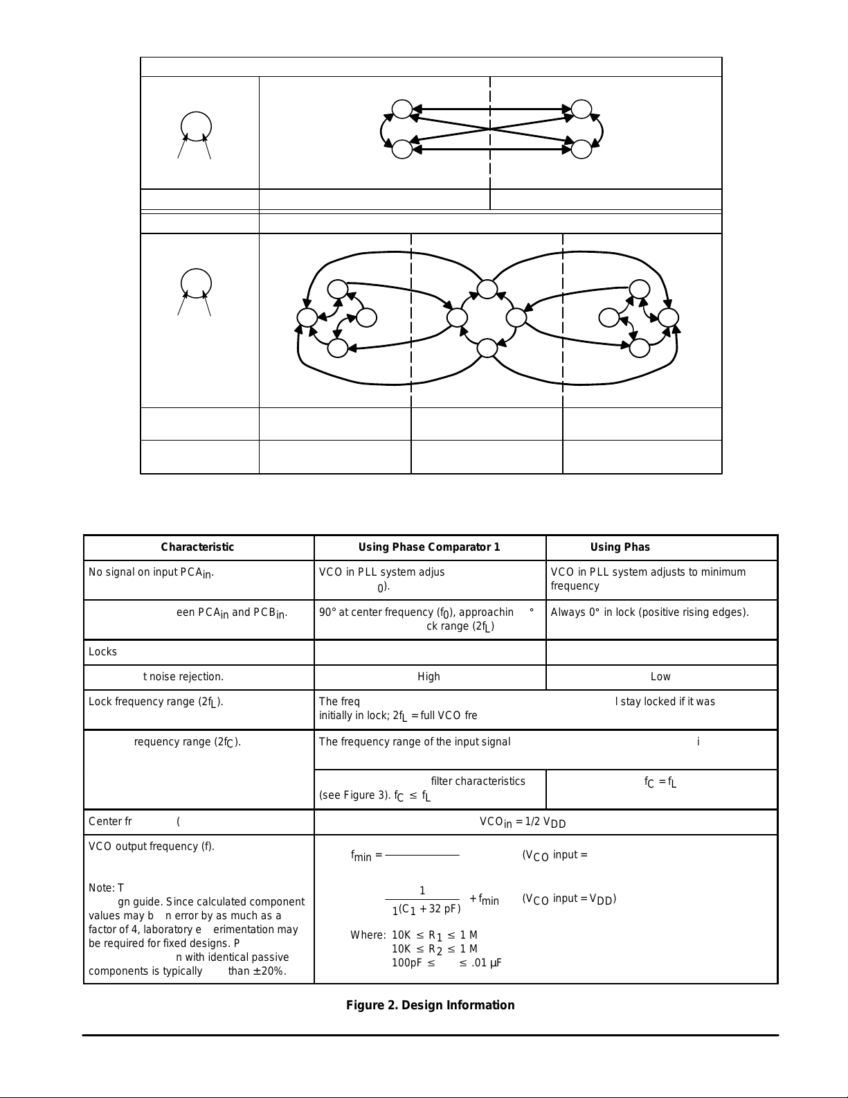
Figure 1. Phase Comparators State Diagrams
PHASE COMPARATOR 1
Input Stage
PCA
in
X X
PCB
in
00 01
11 10
PC1
out
0 1
PHASE COMPARATOR 2
Input Stage
PCA
in
X X
PCB
in
PC2
out
0 1
3–State
Output Disconnected
LD
(Lock Detect)
0 01
Refer to Waveforms in Figure 3.
00
01 10
11
00
10 01
11
00
01 10
11
Characteristic
Using Phase Comparator 1
Using Phase Comparator 2
No signal on input PCAin.
VCO in PLL system adjusts to center
frequency (f0).
VCO in PLL system adjusts to minimum
frequency (f
min
).
Phase angle between PCAin and PCBin.
90° at center frequency (f0), approaching 0
_
and 180° at ends of lock range (2fL)
Always 0_ in lock (positive rising edges).
Locks on harmonics of center frequency.
Yes
No
Signal input noise rejection.
High
Low
Lock frequency range (2fL).
The frequency range of the input signal on which the loop will stay locked if it was
initially in lock; 2fL = full VCO frequency range = f
max
– f
min
.
The frequency range of the input signal on which the loop will lock if it was initially
out of lock.
Depends on low–pass filter characteristics
(see Figure 3). fC v f
L
fC = f
L
Center frequency (f0).
The frequency of VCO
out
, when VCOin = 1/2 V
DD
VCO output frequency (f).
Note: These equations are intended to be
a design guide. Since calculated component
values may be in error by as much as a
factor of 4, laboratory experimentation may
be required for fixed designs. Part to part
frequency variation with identical passive
components is typically less than ± 20%.
Where: 10K v R1 v 1 M
10K v R2 v 1 M
100pF v C1 v .01 µF
Figure 2. Design Information
+ f
min
f
min
= (VCO input = VSS)
R2(C1 + 32 pF)
1
f
max
=
R1(C1 + 32 pF)
1
(VCO input = VDD)
Capture frequency range (2fC).
Page 5
MOTOROLA CMOS LOGIC DATA
5
MC14046B
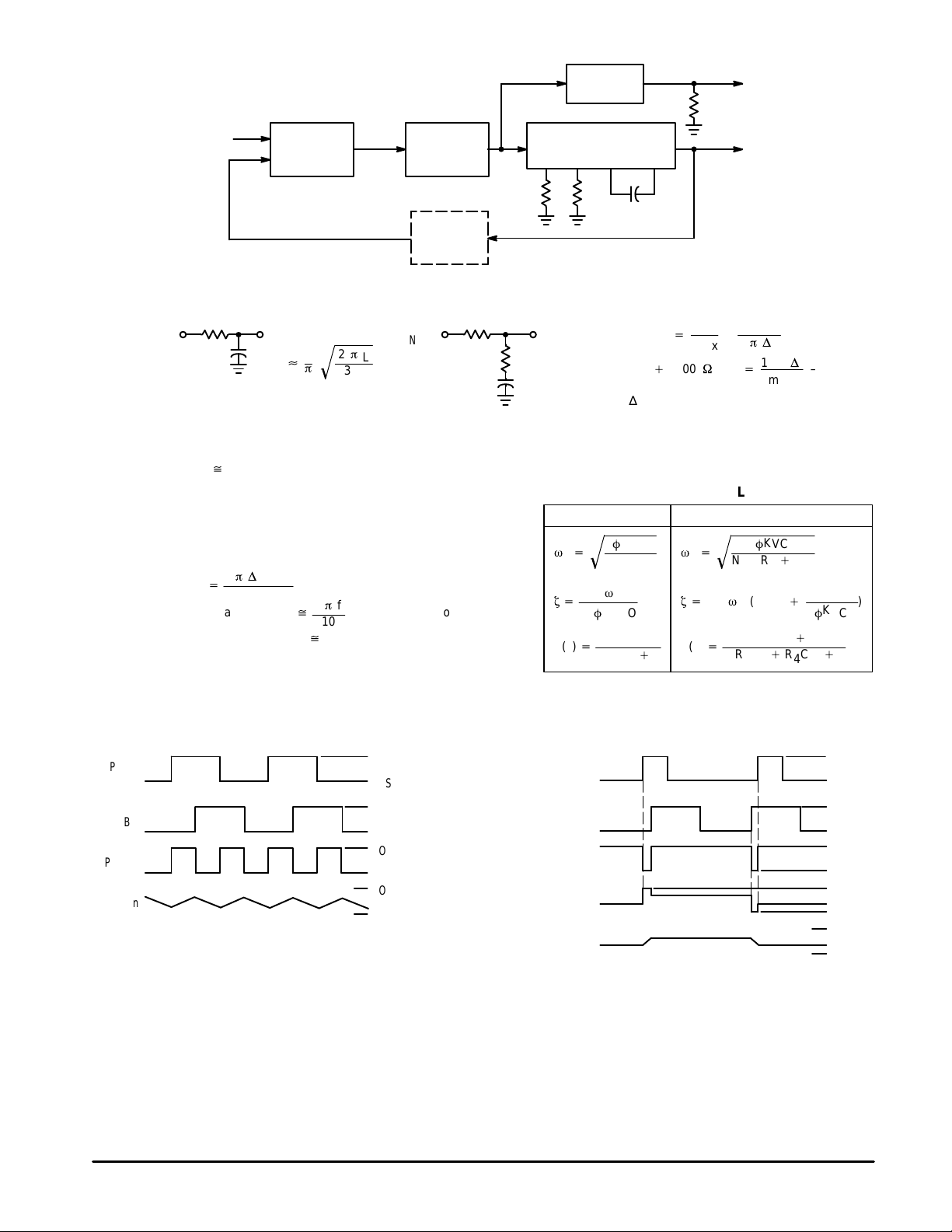
Typical Low–Pass Filters
NOTE: Sometimes R3 is split into two series resistors each R3 ÷ 2. A capacitor CC is then placed from the midpoint to ground. The value for
CC should be such that the corner frequency of this network does not significantly affect ωn. In Figure B, the ratio of R3 to R4 sets the
damping, R4 ^ (0.1)(R3) for optimum results.
Figure 3. General Phase–Locked Loop Connections and Waveforms
Waveforms
Note: for further information, see:
(1) F. Gardner, “Phase–Lock Techniques”, John Wiley and Son, New York, 1966.
(2) G. S. Moschytz, “Miniature RC Filters Using Phase–Locked Loop”, BSTJ, May, 1965.
(3) Garth Nash, “Phase–Lock Loop Design Fundamentals”, AN–535, Motorola Inc.
(4) A. B. Przedpelski, “Phase–Locked Loop Design Articles”, AR254, reprinted by Motorola Inc.
PCA
in
@ FREQUENCY f
′
PCB
in
14
3
PHASE
COMPARATOR
EXTERNAL
LOW–PASS
FILTER
VCO
2 OR 13
PC1
out
OR
PC2
out
VCO
in
9
9
10
4
EXTERNAL
÷
N
COUNTER
R1 R2
11 12 6 7
CIACI
B
CI
SF
out
R
SF
VCO
out
@ FREQUENCY Nf
′
= f
(a)
INPUT
R3
OUTPUT
C2
2fC[
1
p
2pf
L
R3 C2
Ǹ
(a)
INPUT
R3
OUTPUT
R4
C2
Typically:
R4C2+
6N
f
max
–
N
2
p D
f
(R3)
3,000W) C2+
100NDf
f
max
2
– R4C
2
∆ f = f
max
– f
min
Definitions: N = Total division ratio in feedback loop
Kφ = VDD/π for Phase Comparator 1
Kφ = VDD/4 π for Phase Comparator 2
K
VCO
+
2
p D
f
VCO
VDD– 2 V
2pf
r
10
for a typical design ωn
^
(at phase detector input)
ζ ^ 0.707
LOW–PASS FILTER
Filter A Filter B
wn+
KfK
VCO
NR3C
2
Ǹ
z
+
N
w
n
2KfK
VCO
F(s)
+
1
R3C2S)1
wn+
KfK
VCO
NC2(R3)
R
4
)
Ǹ
z+0.5
wn(R3C2)
N
KfK
VCO
)
F(s)
+
R3C2S)1
S(R3C2)
R4C2))1
PCA
in
PCB
in
PC1
out
VCO
in
V
DD
V
SS
V
OH
V
OL
V
OH
V
OL
V
OH
V
OL
PCA
in
PCB
in
PC2
out
VCO
in
LD
V
DD
V
SS
V
OH
V
OL
V
OH
V
OL
V
OH
V
OL
V
OL
V
OH
Phase Comparator 1 Phase Comparator 2
SOURCE
FOLLOWER
Page 6
MOTOROLA CMOS LOGIC DATAMC14046B
6
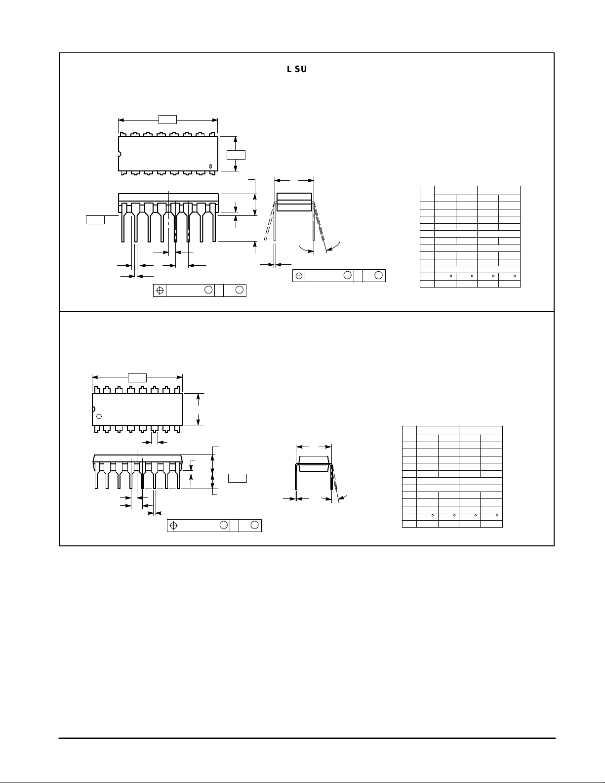
OUTLINE DIMENSIONS
P SUFFIX
PLASTIC DIP PACKAGE
CASE 648–08
ISSUE R
NOTES:
1. DIMENSIONING AND TOLERANCING PER ANSI
Y14.5M, 1982.
2. CONTROLLING DIMENSION: INCH.
3. DIMENSION L TO CENTER OF LEADS WHEN
FORMED PARALLEL.
4. DIMENSION B DOES NOT INCLUDE MOLD FLASH.
5. ROUNDED CORNERS OPTIONAL.
–A–
B
F
C
S
H
G
D
J
L
M
16 PL
SEATING
1 8
916
K
PLANE
–T–
M
A
M
0.25 (0.010) T
DIM MIN MAX MIN MAX
MILLIMETERSINCHES
A 0.740 0.770 18.80 19.55
B 0.250 0.270 6.35 6.85
C 0.145 0.175 3.69 4.44
D 0.015 0.021 0.39 0.53
F 0.040 0.70 1.02 1.77
G 0.100 BSC 2.54 BSC
H 0.050 BSC 1.27 BSC
J 0.008 0.015 0.21 0.38
K 0.110 0.130 2.80 3.30
L 0.295 0.305 7.50 7.74
M 0 10 0 10
S 0.020 0.040 0.51 1.01
____
L SUFFIX
CERAMIC DIP PACKAGE
CASE 620–10
ISSUE V
NOTES:
1. DIMENSIONING AND TOLERANCING PER
ANSI Y14.5M, 1982.
2. CONTROLLING DIMENSION: INCH.
3. DIMENSION L TO CENTER OF LEAD WHEN
FORMED PARALLEL.
4. DIMENSION F MAY NARROW TO 0.76 (0.030)
WHERE THE LEAD ENTERS THE CERAMIC
BODY.
–A–
–B–
–T–
F
E
G
N
K
C
SEATING
PLANE
16 PLD
S
A
M
0.25 (0.010) T
16 PLJ
S
B
M
0.25 (0.010) T
M
L
DIM MIN MAX MIN MAX
MILLIMETERSINCHES
A 0.750 0.785 19.05 19.93
B 0.240 0.295 6.10 7.49
C ––– 0.200 ––– 5.08
D 0.015 0.020 0.39 0.50
E 0.050 BSC 1.27 BSC
F 0.055 0.065 1.40 1.65
G 0.100 BSC 2.54 BSC
H 0.008 0.015 0.21 0.38
K 0.125 0.170 3.18 4.31
L 0.300 BSC 7.62 BSC
M 0 15 0 15
N 0.020 0.040 0.51 1.01
_ _ _ _
16 9
1 8
Page 7
MOTOROLA CMOS LOGIC DATA
7
MC14046B
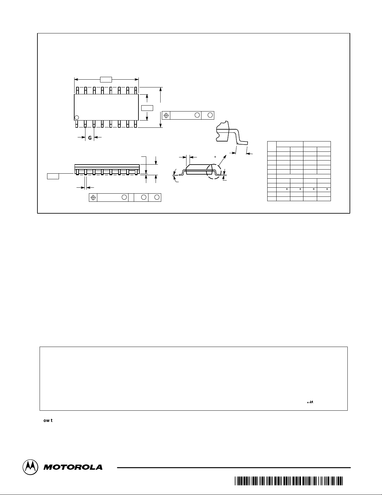
OUTLINE DIMENSIONS
D SUFFIX
PLASTIC SOIC PACKAGE
CASE 751B–05
ISSUE J
NOTES:
1. DIMENSIONING AND TOLERANCING PER ANSI
Y14.5M, 1982.
2. CONTROLLING DIMENSION: MILLIMETER.
3. DIMENSIONS A AND B DO NOT INCLUDE
MOLD PROTRUSION.
4. MAXIMUM MOLD PROTRUSION 0.15 (0.006)
PER SIDE.
5. DIMENSION D DOES NOT INCLUDE DAMBAR
PROTRUSION. ALLOWABLE DAMBAR
PROTRUSION SHALL BE 0.127 (0.005) TOTAL
IN EXCESS OF THE D DIMENSION AT
MAXIMUM MATERIAL CONDITION.
1 8
16 9
SEATING
PLANE
F
J
M
R
X 45
_
G
8 PLP
–B–
–A–
M
0.25 (0.010) B
S
–T–
D
K
C
16 PL
S
B
M
0.25 (0.010) A
S
T
DIM MIN MAX MIN MAX
INCHESMILLIMETERS
A 9.80 10.00 0.386 0.393
B 3.80 4.00 0.150 0.157
C 1.35 1.75 0.054 0.068
D 0.35 0.49 0.014 0.019
F 0.40 1.25 0.016 0.049
G 1.27 BSC 0.050 BSC
J 0.19 0.25 0.008 0.009
K 0.10 0.25 0.004 0.009
M 0 7 0 7
P 5.80 6.20 0.229 0.244
R 0.25 0.50 0.010 0.019
_ _ _ _
How to reach us:
USA/EUROPE/Locations Not Listed: Motorola Literature Distribution; JAPAN: Nippon Motorola Ltd.; Tatsumi–SPD–JLDC, 6F Seibu–Butsuryu–Center,
P.O. Box 20912; Phoenix, Arizona 85036. 1–800–441–2447 or 602–303–5454 3–14–2 Tatsumi Koto–Ku, Tokyo 135, Japan. 03–81–3521–8315
MFAX: [email protected] – TOUCHTONE 602–244–6609 ASIA/PACIFIC: Motorola Semiconductors H.K. Ltd.; 8B Tai Ping Industrial Park,
INTERNET: http://Design–NET.com 51 Ting Kok Road, Tai Po, N.T., Hong Kong. 852–26629298
Motorola reserves the right to make changes without further notice to any products herein. Motorola makes no warranty , representation or guarantee regarding
the suitability of its products for any particular purpose, nor does Motorola assume any liability arising out of the application or use of any product or circuit,
and specifically disclaims any and all liability, including without limitation consequential or incidental damages. “Typical” parameters which may be provided
in Motorola data sheets and/or specifications can and do vary in different applications and actual performance may vary over time. All operating parameters,
including “Typicals” must be validated for each customer application by customer’s technical experts. Motorola does not convey any license under its patent
rights nor the rights of others. Motorola products are not designed, intended, or authorized for use as components in systems intended for surgical implant
into the body, or other applications intended to support or sustain life, or for any other application in which the failure of the Motorola product could create a
situation where personal injury or death may occur. Should Buyer purchase or use Motorola products for any such unintended or unauthorized application,
Buyer shall indemnify and hold Motorola and its officers, employees, subsidiaries, affiliates, and distributors harmless against all claims, costs, damages, and
expenses, and reasonable attorney fees arising out of, directly or indirectly, any claim of personal injury or death associated with such unintended or
unauthorized use, even if such claim alleges that Motorola was negligent regarding the design or manufacture of the part. Motorola and are registered
trademarks of Motorola, Inc. Motorola, Inc. is an Equal Opportunity/Affirmative Action Employer .
MC14046B/D
*MC14046B/D*
◊
Page 8

This datasheet has been download from:
www.datasheetcatalog.com
Datasheets for electronics components.
 Loading...