

Page 1
MOTOROLA CMOS LOGIC DATA
135
MC14034B
The MC14034B is a bidirectional 8–bit static parallel/serial, input/output
bus register. The device contains two sets of input/output lines which allows
the bidirectional transfer of data between two buses; the conversion of serial
data t o parallel form, or t he conversion of parallel data to serial form.
Additionally the serial data input allows data to be entered shift/right, while
shift/left can be accomplished by hard–wiring each parallel output to the
previous parallel bit input.
Other useful applications for this device include pseudo–random code
generation, sample and hold register, frequency and phase–comparator,
address or buffer register, and serial/parallel input/output conversions.
• Bidirectional Parallel Data Input
• Diode Protection on All Inputs
• Supply Voltage Range = 3.0 Vdc to 18 Vdc
• Capable of Driving Two Low–power TTL Loads or One Low–power
Schottky TTL Load Over the Rated Temperature Range.
• Pin–for–Pin Replacement for CD4034B.
MAXIMUM RATINGS* (Voltages Referenced to V
SS
)
Symbol
Parameter
Value
Unit
V
DD
DC Supply Voltage
– 0.5 to + 18.0
V
Vin, V
out
Input or Output Voltage (DC or Transient)
– 0.5 to VDD + 0.5
V
lin, l
out
Input or Output Current (DC or Transient),
per Pin
± 10
mA
P
D
Power Dissipation, per Package†
500
mW
T
stg
Storage Temperature
– 65 to + 150
_
C
T
L
Lead Temperature (8–Second Soldering)
260
_
C
*Maximum Ratings are those values beyond which damage to the device may occur.
†Temperature Derating:
Plastic “P and D/DW” Packages: – 7.0 mW/_C From 65_C To 125_C
Ceramic “L” Packages: – 12 mW/_C From 100_C To 125_C
This device contains protection circuitry to guard against damage
due to high static voltages or electric fields. However, precautions must
be taken to avoid applications of any voltage higher than maximum rated
voltages to this high-impedance circuit. For proper operation, Vin and
V
out
should be constrained to the range VSS ≤ (Vin or V
out
) ≤ VDD.
Unused inputs must always be tied to an appropriate logic voltage
level (e.g., either VSS or VDD). Unused outputs must be left open.
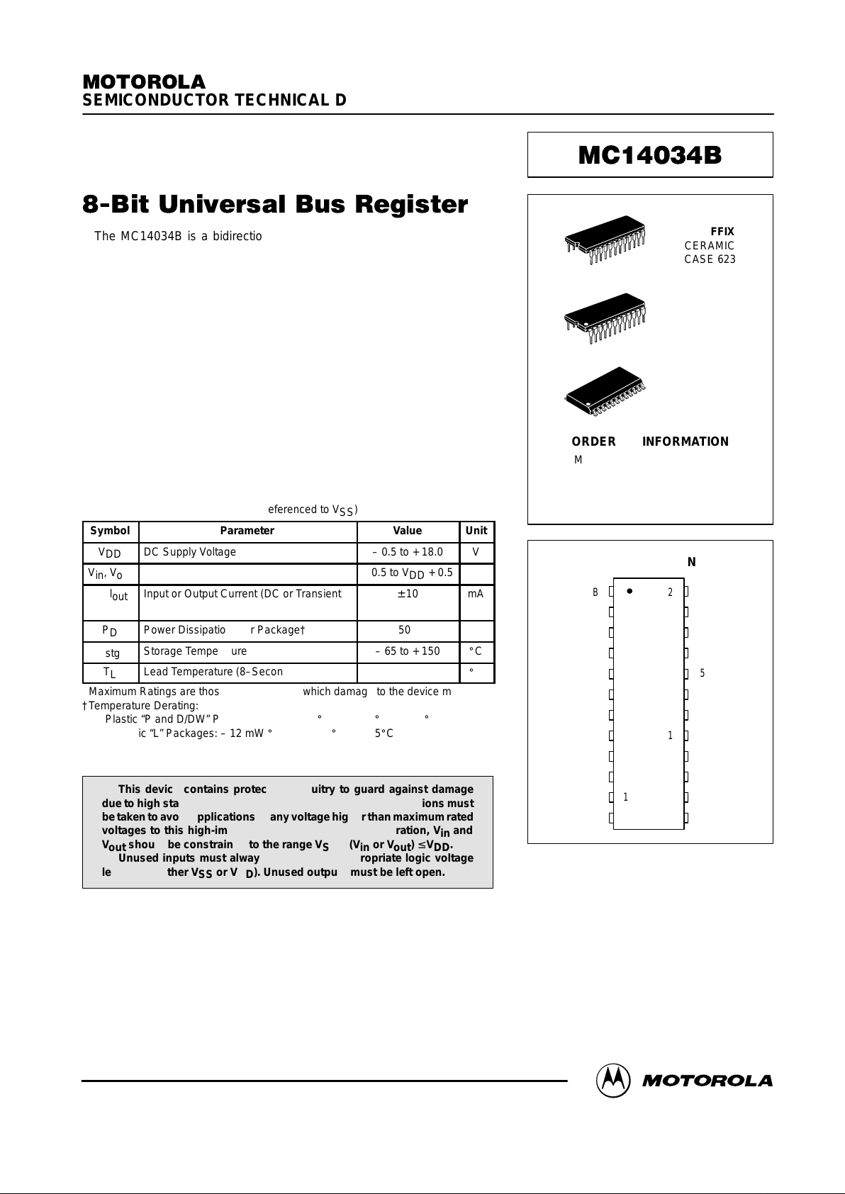
SEMICONDUCTOR TECHNICAL DATA
Motorola, Inc. 1995
REV 3
1/94
L SUFFIX
CERAMIC
CASE 623
ORDERING INFORMATION
MC14XXXBCP Plastic
MC14XXXBCL Ceramic
MC14XXXBDW SOIC
TA = – 55° to 125°C for all packages.
P SUFFIX
PLASTIC
CASE 709
DW SUFFIX
SOIC
CASE 751E
PIN ASSIGNMENT
B3
B5
B6
B7
B8
B1
B2
B4 A5
A6
A7
A8
V
DD
C
A1
A2
5
4
3
2
1
10
9
8
7
6
14
15
16
17
18
19
20
13
11
12
21
22
23
24
P/S
A/S
A3
A4
A/B
V
SS
D
S
A ENABLE
Page 2
MOTOROLA CMOS LOGIC DATAMC14034B
136
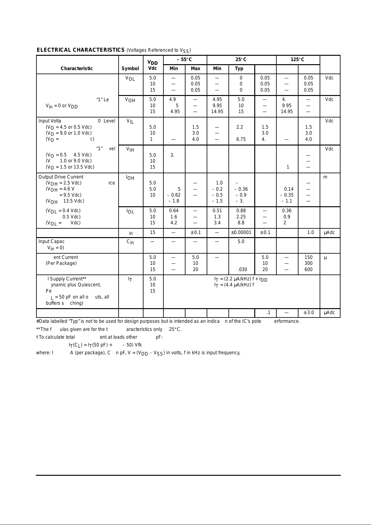
ELECTRICAL CHARACTERISTICS (Voltages Referenced to V
SS
)
V
– 55_C
25_C
125_C
Characteristic
Symbol
V
DD
Vdc
Min
Max
Min
Typ #
Max
Min
ÎÎÎ
ÎÎÎ
ÎÎÎ
Max
Unit
Output Voltage
“0” Level
Vin = VDD or 0
V
OL
5.0
10
15
—
—
—
0.05
0.05
0.05
—
—
—
0
0
0
0.05
0.05
0.05
—
—
—
ÎÎÎ
ÎÎÎ
ÎÎÎ
ÎÎÎ
0.05
0.05
0.05
Vdc
“1” Level
Vin = 0 or V
DD
V
OH
5.0
10
15
4.95
9.95
14.95
—
—
—
4.95
9.95
14.95
5.0
10
15
—
—
—
4.95
9.95
14.95
ÎÎÎ
ÎÎÎ
ÎÎÎ
ÎÎÎ
ÎÎÎ
—
—
—
Vdc
Input Voltage
“0” Level
(VO = 4.5 or 0.5 Vdc)
(VO = 9.0 or 1.0 Vdc)
(VO = 13.5 or 1.5 Vdc)
V
IL
5.0
10
15
—
—
—
1.5
3.0
4.0
—
—
—
2.25
4.50
6.75
1.5
3.0
4.0
—
—
—
ÎÎÎ
ÎÎÎ
ÎÎÎ
ÎÎÎ
ÎÎÎ
1.5
3.0
4.0
Vdc
“1” Level
(VO = 0.5 or 4.5 Vdc)
(VO = 1.0 or 9.0 Vdc)
(VO = 1.5 or 13.5 Vdc)
V
IH
5.0
10
15
3.5
7.0
11
—
—
—
3.5
7.0
11
2.75
5.50
8.25
—
—
—
3.5
7.0
11
ÎÎÎ
ÎÎÎ
ÎÎÎ
ÎÎÎ
ÎÎÎ
—
—
—
Vdc
Output Drive Current
(VOH = 2.5 Vdc) Source
(VOH = 4.6 Vdc)
(VOH = 9.5 Vdc)
(VOH = 13.5 Vdc)
I
OH
5.0
5.0
10
15
– 1.2
– 0.25
– 0.62
– 1.8
—
—
—
—
– 1.0
– 0.2
– 0.5
– 1.5
– 1.7
– 0.36
– 0.9
– 3.5
—
—
—
—
– 0.7
– 0.14
– 0.35
– 1.1
ÎÎÎ
ÎÎÎ
ÎÎÎ
ÎÎÎ
ÎÎÎ
—
—
—
—
mAdc
(VOL = 0.4 Vdc) Sink
(VOL = 0.5 Vdc)
(VOL = 1.5 Vdc)
I
OL
5.0
10
15
0.64
1.6
4.2
—
—
—
0.51
1.3
3.4
0.88
2.25
8.8
—
—
—
0.36
0.9
2.4
ÎÎÎ
ÎÎÎ
ÎÎÎ
ÎÎÎ
ÎÎÎ
—
—
—
mAdc
Input Current
I
in
15
—
± 0.1
—
±0.00001
± 0.1
—
ÎÎÎ
ÎÎÎ
ÎÎÎ
± 1.0
µAdc
Input Capacitance
(Vin = 0)
C
in
—
—
—
—
5.0
7.5
—
ÎÎÎ
ÎÎÎ
ÎÎÎ
—
pF
Quiescent Current
(Per Package)
I
DD
5.0
10
15
—
—
—
5.0
10
20
—
—
—
0.010
0.020
0.030
5.0
10
20
—
—
—
ÎÎÎ
ÎÎÎ
ÎÎÎ
ÎÎÎ
ÎÎÎ
150
300
600
µAdc
Total Supply Current**†
(Dynamic plus Quiescent,
Per Package)
(CL = 50 pF on all outputs, all
buffers switching)
I
T
5.0
10
15
IT = (2.2 µA/kHz) f + I
DD
IT = (4.4 µA/kHz) f + I
DD
IT = (6.6 µA/kHz) f + I
DD
µAdc
3–State Output Leakage Current
I
TL
15
—
± 0.1
—
± 0.0001
± 0.1
—
ÎÎÎ
ÎÎÎ
ÎÎÎ
± 3.0
µAdc
#Data labelled “Typ” is not to be used for design purposes but is intended as an indication of the IC’s potential performance.
**The formulas given are for the typical characteristics only at 25_C.
†To calculate total supply current at loads other than 50 pF:
IT(CL) = IT(50 pF) + (CL – 50) Vfk
where: IT is in µA (per package), CL in pF, V = (VDD – VSS) in volts, f in kHz is input frequency, and k = 0.004.
Page 3
MOTOROLA CMOS LOGIC DATA
137
MC14034B
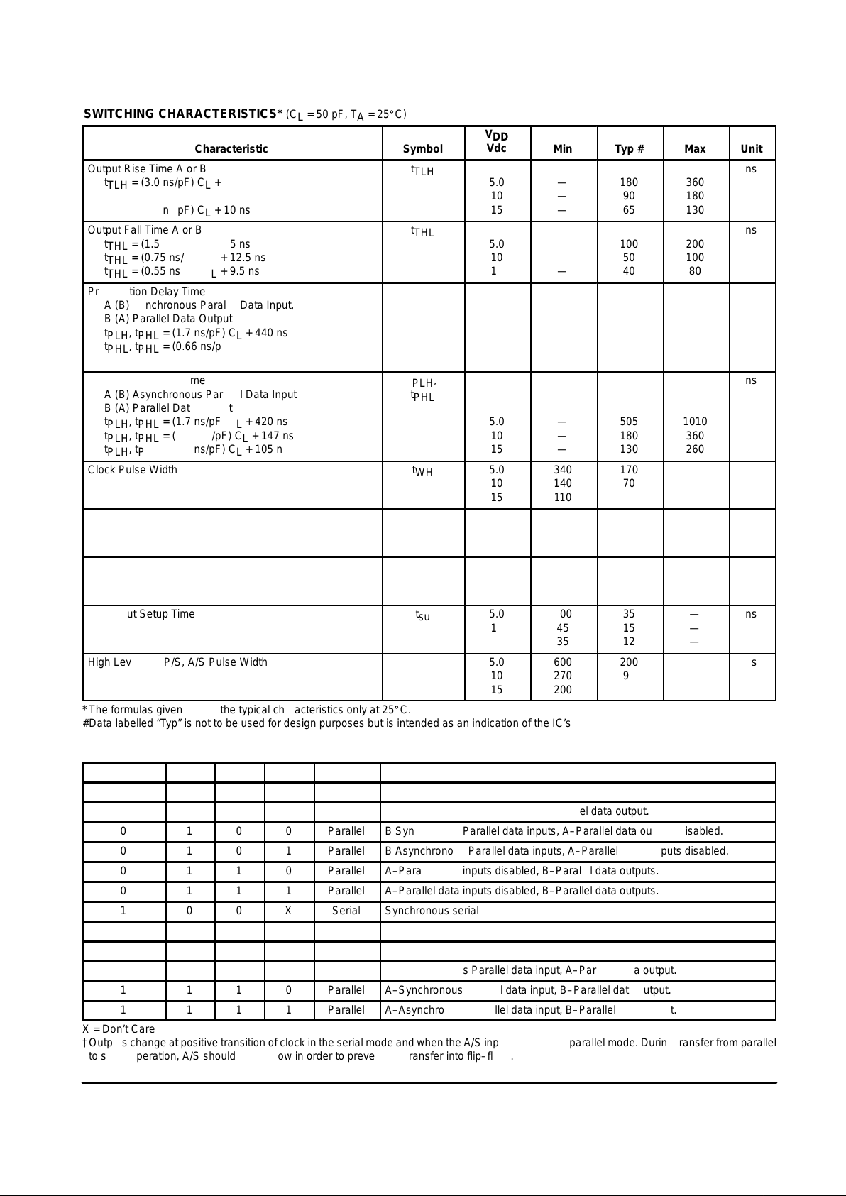
SWITCHING CHARACTERISTICS* (C
L
= 50 pF, TA = 25_C)
Characteristic
ÎÎÎÎ
ÎÎÎÎ
ÎÎÎÎ
ÎÎÎÎ
Symbol
V
DD
Vdc
ÎÎÎÎ
ÎÎÎÎ
ÎÎÎÎ
ÎÎÎÎ
Min
Typ #
Max
Unit
Output Rise Time A or B
t
TLH
= (3.0 ns/pF) CL + 30 ns
t
TLH
= (1.5 ns/pF) CL + 15 ns
t
TLH
= (1.1 ns/pF) CL + 10 ns
ÎÎÎÎ
ÎÎÎÎ
ÎÎÎÎ
ÎÎÎÎ
ÎÎÎÎ
t
TLH
5.0
10
15
ÎÎÎÎ
ÎÎÎÎ
ÎÎÎÎ
ÎÎÎÎ
ÎÎÎÎ
—
—
—
180
90
65
360
180
130
ns
Output Fall Time A or B
t
THL
= (1.5 ns/pF) CL + 25 ns
t
THL
= (0.75 ns/pF) CL + 12.5 ns
t
THL
= (0.55 ns/pF) CL + 9.5 ns
ÎÎÎÎ
ÎÎÎÎ
ÎÎÎÎ
ÎÎÎÎ
t
THL
5.0
10
15
ÎÎÎÎ
ÎÎÎÎ
ÎÎÎÎ
ÎÎÎÎ
—
—
—
100
50
40
200
100
80
ns
Propagation Delay Time
A (B) Synchronous Parallel Data Input,
B (A) Parallel Data Output
t
PLH
, t
PHL
= (1.7 ns/pF) CL + 440 ns
t
PHL
, t
PHL
= (0.66 ns/pF) CL + 172 ns
t
PLH
, t
PHL
= (0.5 ns/pF) CL + 120 ns
ÎÎÎÎ
ÎÎÎÎ
ÎÎÎÎ
ÎÎÎÎ
ÎÎÎÎ
ÎÎÎÎ
ÎÎÎÎ
t
PLH
,
t
PHL
5.0
10
15
ÎÎÎÎ
ÎÎÎÎ
ÎÎÎÎ
ÎÎÎÎ
ÎÎÎÎ
ÎÎÎÎ
ÎÎÎÎ
—
—
—
525
205
145
1050
410
290
ns
Propagation Delay Time
A (B) Asynchronous Parallel Data Input
B (A) Parallel Data Output
t
PLH
, t
PHL
= (1.7 ns/pF) CL + 420 ns
t
PLH
, t
PHL
= (0.66 ns/pF) CL + 147 ns
t
PLH
, t
PHL
= (0.5 ns/pF) CL + 105 ns
ÎÎÎÎ
ÎÎÎÎ
ÎÎÎÎ
ÎÎÎÎ
ÎÎÎÎ
ÎÎÎÎ
t
PLH
,
t
PHL
5.0
10
15
ÎÎÎÎ
ÎÎÎÎ
ÎÎÎÎ
ÎÎÎÎ
ÎÎÎÎ
ÎÎÎÎ
—
—
—
505
180
130
1010
360
260
ns
Clock Pulse Width
ÎÎÎÎ
ÎÎÎÎ
ÎÎÎÎ
ÎÎÎÎ
t
WH
5.0
10
15
ÎÎÎÎ
ÎÎÎÎ
ÎÎÎÎ
ÎÎÎÎ
340
140
110
170
70
55
—
—
—
ns
Clock Pulse Frequency
ÎÎÎÎ
ÎÎÎÎ
ÎÎÎÎ
ÎÎÎÎ
f
cl
5.0
10
15
ÎÎÎÎ
ÎÎÎÎ
ÎÎÎÎ
ÎÎÎÎ
—
—
—
2.5
6.0
8.0
1.2
3.0
4.0
MHz
Clock Pulse Rise
ÎÎÎÎ
ÎÎÎÎ
ÎÎÎÎ
ÎÎÎÎ
ÎÎÎÎ
t
TLH
, t
THL
5.0
10
15
ÎÎÎÎ
ÎÎÎÎ
ÎÎÎÎ
ÎÎÎÎ
ÎÎÎÎ
—
—
—
—
—
—
15
5
4
µs
A, B Input Setup Time
ÎÎÎÎ
ÎÎÎÎ
ÎÎÎÎ
ÎÎÎÎ
t
su
5.0
10
15
ÎÎÎÎ
ÎÎÎÎ
ÎÎÎÎ
ÎÎÎÎ
100
45
35
35
15
12
—
—
—
ns
High Level SE, P/S, A/S Pulse Width
ÎÎÎÎ
ÎÎÎÎ
ÎÎÎÎ
ÎÎÎÎ
t
WH
5.0
10
15
ÎÎÎÎ
ÎÎÎÎ
ÎÎÎÎ
ÎÎÎÎ
600
270
200
200
90
80
—
—
—
ns
*The formulas given are for the typical characteristics only at 25_C.
#Data labelled “Typ” is not to be used for design purposes but is intended as an indication of the IC’s potential performance.
TRUTH TABLE
“A” Enable P/S A/B A/S Mode Operation†
0 0 0 X Serial Synchronous Serial data input, A and B Parallel data outputs disabled.
0 0 1 X Serial Synchronous Serial data input, B–Parallel data output.
0 1 0 0 Parallel B Synchronous Parallel data inputs, A–Parallel data outputs disabled.
0 1 0 1 Parallel B Asynchronous Parallel data inputs, A–Parallel data outputs disabled.
0 1 1 0 Parallel A–Parallel data inputs disabled, B–Parallel data outputs.
0 1 1 1 Parallel A–Parallel data inputs disabled, B–Parallel data outputs.
1 0 0 X Serial Synchronous serial data input, A–Parallel data output.
1 0 1 X Serial Synchronous serial data input, B–Parallel data output.
1 1 0 0 Parallel B–Synchronous Parallel data input, A–Parallel data output.
1 1 0 1 Parallel B–Asynchronous Parallel data input, A–Parallel data output.
1 1 1 0 Parallel A–Synchronous Parallel data input, B–Parallel data output.
1 1 1 1 Parallel A–Asynchronous Parallel data input, B–Parallel data output.
X = Don’t Care
†Outputs change at positive transition of clock in the serial mode and when the A/S input is low in the parallel mode. During transfer from parallel
to serial operation, A/S should remain low in order to prevent DS transfer into flip–flops.
Page 4

MOTOROLA CMOS LOGIC DATAMC14034B
138
EXPANDED BLOCK DIAGRAM
SERIAL DATA INPUT
PARALLEL/SERIAL P/S
A/B
ENABLE A
ASYN/SYN A/S
CLOCK
CONTROL
LOGIC
A1 A2 A3 A4 A5 A6 A7 A8
B1 B2 B3 B4 B5 B6 B7 B8
DATA
DATA
8–BIT REGISTER
OPERATING CHARACTERISTICS
The MC14034B is composed of eight register cells connected in cascade with additional control logic. Each register
cell is composed of one “D” master–slave flip–flop with separate internal clocks, and two data transfer gates allowing the
data to be transferred bi–directionally from bus A to bus B
and from bus B to bus A, and to be memorized. Besides the
single phase clock and the serial data inputs, the control logic provides four other features:
A Enable Input — When high, this input enables the bus A
data lines.
A/B Input (Data A or B) — This input controls the direction of data flow: when high, the data flows from bus A to bus
B; when low, the data flows from bus B to bus A.
P/S Input (Parallel/Serial) — This input controls the data
input mode (parallel or serial). When high, the data is transferred to the register in a parallel asynchronous mode or a
parallel synchronous mode (positive clock transition). When
low, the data is entered into the register in a serial synchronous mode (positive clock transition).
A/S Input (Asynchronous/Synchronous to the Clock)
— When this input is high, the data is transferred indepen-
dently from the clock rate; when low, the clock is enabled and
the data is transferred synchronously.
LOGIC DIAGRAM
A ENABLE 9
A/B 11
SERIAL DATA 10
PARALLEL SERIAL 13
ASYN/SYN 14
CLOCK 15
C
M
*D FLIP FLOP
V
DD
C
S
V
DD
A1
16
A217A318A419A520A621A7
22
A8
23
V
DD
6 STAGES
(SAME AS
STAGE 1)
*D
FLIP–
FLOP
D
CMC
S
Q
8
B1
7B26B35B44B53B62
B7
1
B8
Page 5

MOTOROLA CMOS LOGIC DATA
139
MC14034B
Figure 1. Propagation Delay and Transition Times Waveforms
INPUT
A(B)
CLOCK
OUTPUT
B(A)
t
su
20 ns
20 ns
50%
90%
10%
t
PLH
t
PHL
t
TLH
t
THL
PROPAGATION AND TRANSITION TIME TEST CIRCUITS
Figure 2. A Synchronous Data Input, B Parallel
Data Output and Setup Time
Figure 3. B Synchronous Data Input, A Parallel
Data Output and Setup Time
PROGRAMMABLE
PULSE
GENERATOR
PROGRAMMABLE
PULSE
GENERATOR
C
L
C
L
V
SS
V
DD
V
DD
V
SS
A1 A2 A3 A4 A5 A6 A7 A8
A ENABLE
P/S
D
S
A/B
A/S
C
B1 B2 B3 B4 B5 B6 B7 B8
A1 A2 A3 A4 A5 A6 A7 A8
A ENABLE
P/S
D
S
A/B
A/S
C
B1 B2 B3 B4 B5 B6 B7 B8
Page 6

MOTOROLA CMOS LOGIC DATAMC14034B
140
Figure 4. Power Dissipation Test Circuit and Waveforms
PROGRAMMABLE
PULSE
GENERATOR
C
L
V
DD
V
SS
A1 A2 A3 A4 A5 A6 A7 A8
AE
B1 B2 B3 B4 B5 B6 B7 B8
P/S
D
S
A/B
A/S
C
C
L
C
L
C
L
C
L
C
L
C
L
C
L
V
DD
V
SS
V
DD
V
SS
20 ns
20 ns
90%
10%
50%
t
WH
t
WL
90%
10%
50%
20 ns20 ns
D
S
CLOCK
1/f
tWH = tWL = 50% DUTY CYCLE
Figure 5. 16–Bit Parallel In/Parallel Out, Parallel In/Serial Out,
Serial In/Parallel Out, Serial In/Serial Out Register
V
DD
V
DD
SERIAL
DATA
V
DD
P/S
A/S
CLOCK
SERIAL
DATA
SERIAL
DATA
V
DD
A ENABLE
P/S
D
S
A/B
A/S
C
B1A1B2 B3 B4 B5 B6 B7 B8
A2 A3 A4 A5 A6 A7 A8
MC14034B
A ENABLE
P/S
D
S
A/B
A/S
C
B1A1B2 B3 B4 B5 B6 B7 B8
A2 A3 A4 A5 A6 A7 A8
Page 7

MOTOROLA CMOS LOGIC DATA
141
MC14034B
Figure 6. Shift Right/Shift Left with Parallel Inputs
A “High” (“Low”) on the Shift Left/Shift Right input allows serial data on the Shift Left Input (Shift Right Input) to enter the register
on the positive transition of the lock signal. A “high” on the “A” Enable Input disables the “A” parallel data lines on Reg. 1 and 2
and enables the “A” data lines on registers 3 and 4 and allows parallel data into registers 1 and 2. Other logic schemes may be
used in place of registers 3 and 4 for parallel loading.
When parallel inputs are not used, Reg. 3 and 4 and associated logic are not required.
*Shift left input must be disabled during parallel entry.
A ENABLE
SHIFT LEFT/
SHIFT RIGHT
SHIFT RIGHT
INPUT
CLOCK
A/S PARALLEL
ENTRY
REGISTER 1
MC14034B
SHIFT LEFT OUTPUT
AE
P/S
D
S
A/B
A/S
C
B1 B8
A1 A8
AE
P/S
D
S
A/B
A/S
C
A1 A8
B1 B8
AE
P/S
SHIFT RIGHT
OUTPUT
REGISTER 2
MC14034B
SHIFT LEFT
INPUT*
A/S
COCK
AE
V
DD
V
DD
AE
P/S
D
S
A/B
A/S
C
B1 B8
REGISTER 3
MC14034B
REGISTER 4
MC14034B
A1 A8
AE
P/S
D
S
A/B
A/S
C
B1 B8
A1 A8
Page 8

MOTOROLA CMOS LOGIC DATAMC14034B
142
OUTLINE DIMENSIONS
P SUFFIX
PLASTIC DIP PACKAGE
CASE 709–02
ISSUE C
L SUFFIX
CERAMIC DIP PACKAGE
CASE 623–05
ISSUE M
NOTES:
1. POSITIONAL TOLERANCE OF LEADS (D),
SHALL BE WITHIN 0.25 (0.010) AT MAXIMUM
MATERIAL CONDITION, IN RELATION TO
SEATING PLANE AND EACH OTHER.
2. DIMENSION L TO CENTER OF LEADS WHEN
FORMED PARALLEL.
3. DIMENSION B DOES NOT INCLUDE MOLD
FLASH.
DIM MIN MAX MIN MAX
INCHESMILLIMETERS
A 31.37 32.13 1.235 1.265
B 13.72 14.22 0.540 0.560
C 3.94 5.08 0.155 0.200
D 0.36 0.56 0.014 0.022
F 1.02 1.52 0.040 0.060
G 2.54 BSC 0.100 BSC
H 1.65 2.03 0.065 0.080
J 0.20 0.38 0.008 0.015
K 2.92 3.43 0.115 0.135
L 15.24 BSC 0.600 BSC
M 0 15 0 15
N 0.51 1.02 0.020 0.040
_ _ _ _
1 12
1324
B
H
A
F
D
G
K
SEATING
PLANE
N
C
M
J
L
NOTES:
1. DIMENSION L TO CENTER OF LEADS WHEN
FORMED PARALLEL.
2. LEADS WITHIN 0.13 (0.005) RADIUS OF TRUE
POSITION AT SEATING PLANE AT MAXIMUM
MATERIAL CONDITION (WHEN FORMED
PARALLEL).
1 12
24 13
B
A
SEATING
PLANE
F
D
G
K
N
C
M
J
L
DIM MIN MAX MIN MAX
INCHESMILLIMETERS
A 31.24 32.77 1.230 1.290
B 12.70 15.49 0.500 0.610
C 4.06 5.59 0.160 0.220
D 0.41 0.51 0.016 0.020
F 1.27 1.52 0.050 0.060
G 2.54 BSC 0.100 BSC
J 0.20 0.30 0.008 0.012
K 3.18 4.06 0.125 0.160
L 15.24 BSC 0.600 BSC
M 0 15 0 15
N 0.51 1.27 0.020 0.050
_ _ _ _
Page 9

MOTOROLA CMOS LOGIC DATA
143
MC14034B
OUTLINE DIMENSIONS
DW SUFFIX
PLASTIC SOIC PACKAGE
CASE 751E–04
ISSUE E
NOTES:
1. DIMENSIONING AND TOLERANCING PER ANSI
Y14.5M, 1982.
2. CONTROLLING DIMENSION: MILLIMETER.
3. DIMENSIONS A AND B DO NOT INCLUDE
MOLD PROTRUSION.
4. MAXIMUM MOLD PROTRUSION 0.15 (0.006)
PER SIDE.
5. DIMENSION D DOES NOT INCLUDE DAMBAR
PROTRUSION. ALLOWABLE DAMBAR
PROTRUSION SHALL BE 0.13 (0.005) TOTAL IN
EXCESS OF D DIMENSION AT MAXIMUM
MATERIAL CONDITION.
–A–
–B– P12X
D24X
12
1324
1
M
0.010 (0.25) B
M
S
A
M
0.010 (0.25) B
S
T
–T–
G
22X
SEATING
PLANE
K
C
R
X 45
_
M
F
J
DIM MIN MAX MIN MAX
INCHESMILLIMETERS
A 15.25 15.54 0.601 0.612
B 7.40 7.60 0.292 0.299
C 2.35 2.65 0.093 0.104
D 0.35 0.49 0.014 0.019
F 0.41 0.90 0.016 0.035
G 1.27 BSC 0.050 BSC
J 0.23 0.32 0.009 0.013
K 0.13 0.29 0.005 0.011
M 0 8 0 8
P 10.05 10.55 0.395 0.415
R 0.25 0.75 0.010 0.029
____
How to reach us:
USA/EUROPE/Locations Not Listed: Motorola Literature Distribution; JAPAN: Nippon Motorola Ltd.; Tatsumi–SPD–JLDC, 6F Seibu–Butsuryu–Center,
P.O. Box 20912; Phoenix, Arizona 85036. 1–800–441–2447 or 602–303–5454 3–14–2 Tatsumi Koto–Ku, Tokyo 135, Japan. 03–81–3521–8315
MFAX: RMFAX0@email.sps.mot.com – TOUCHTONE 602–244–6609 ASIA/PACIFIC: Motorola Semiconductors H.K. Ltd.; 8B Tai Ping Industrial Park,
INTERNET: http://Design–NET.com 51 Ting Kok Road, Tai Po, N.T., Hong Kong. 852–26629298
Motorola reserves the right to make changes without further notice to any products herein. Motorola makes no warranty , representation or guarantee regarding
the suitability of its products for any particular purpose, nor does Motorola assume any liability arising out of the application or use of any product or circuit,
and specifically disclaims any and all liability, including without limitation consequential or incidental damages. “Typical” parameters which may be provided
in Motorola data sheets and/or specifications can and do vary in different applications and actual performance may vary over time. All operating parameters,
including “Typicals” must be validated for each customer application by customer’s technical experts. Motorola does not convey any license under its patent
rights nor the rights of others. Motorola products are not designed, intended, or authorized for use as components in systems intended for surgical implant
into the body, or other applications intended to support or sustain life, or for any other application in which the failure of the Motorola product could create a
situation where personal injury or death may occur. Should Buyer purchase or use Motorola products for any such unintended or unauthorized application,
Buyer shall indemnify and hold Motorola and its officers, employees, subsidiaries, affiliates, and distributors harmless against all claims, costs, damages, and
expenses, and reasonable attorney fees arising out of, directly or indirectly, any claim of personal injury or death associated with such unintended or
unauthorized use, even if such claim alleges that Motorola was negligent regarding the design or manufacture of the part. Motorola and are registered
trademarks of Motorola, Inc. Motorola, Inc. is an Equal Opportunity/Affirmative Action Employer .
MC14034B/D
*MC14034B/D*
◊
 Loading...