

Page 1
MOTOROLA CMOS LOGIC DATA
65
MC14016B
The MC14016B quad bilateral switch is constructed with MOS P–channel
and N–channel enhancement mode devices in a single monolithic structure.
Each M C14016B c onsists o f four independent switches c apable of
controlling either digital or analog signals. The quad bilateral switch is used
in s ignal g ating, c hopper, modulator, demodulator and CMOS l ogic
implementation.
• Diode Protection on All Inputs
• Supply Voltage Range = 3.0 Vdc to 18 Vdc
• Linearized Transfer Characteristics
• Low Noise — 12 nV/√Cycle
, f ≥ 1.0 kHz typical
• Pin–for–Pin Replacements for CD4016B, CD4066B (Note improved
transfer characteristic design causes more parasitic coupling
capacitance than CD4016)
• For Lower RON, Use The HC4016 High–Speed CMOS Device or The
MC14066B
• This Device Has Inputs and Outputs Which Do Not Have ESD
Protection. Antistatic Precautions Must Be Taken.
MAXIMUM RATINGS* (Voltages Referenced to V
SS
)
Symbol
Parameter
Value
Unit
V
DD
DC Supply Voltage
– 0.5 to + 18.0
V
Vin, V
out
Input or Output Voltage (DC or Transient)
– 0.5 to VDD + 0.5
V
l
in
Input Current (DC or Transient),
per Control Pin
± 10
mA
I
sw
Switch Through Current
± 25
mA
P
D
Power Dissipation, per Package†
500
mW
T
stg
Storage Temperature
– 65 to + 150
_
C
T
L
Lead Temperature (8–Second Soldering)
260
_
C
*Maximum Ratings are those values beyond which damage to the device may occur.
†Temperature Derating:
Plastic “P and D/DW” Packages: – 7.0 mW/_C From 65_C To 125_C
Ceramic “L” Packages: – 12 mW/_C From 100_C To 125_C
This device contains protection circuitry to guard against damage
due to high static voltages or electric fields. However, precautions must
be taken to avoid applications of any voltage higher than maximum rated
voltages to this high-impedance circuit. For proper operation, Vin and
V
out
should be constrained to the range VSS ≤ (Vin or V
out
) ≤ VDD.
Unused inputs must always be tied to an appropriate logic voltage
level (e.g., either VSS or VDD). Unused outputs must be left open.
SEMICONDUCTOR TECHNICAL DATA
Motorola, Inc. 1995
REV 3
1/94
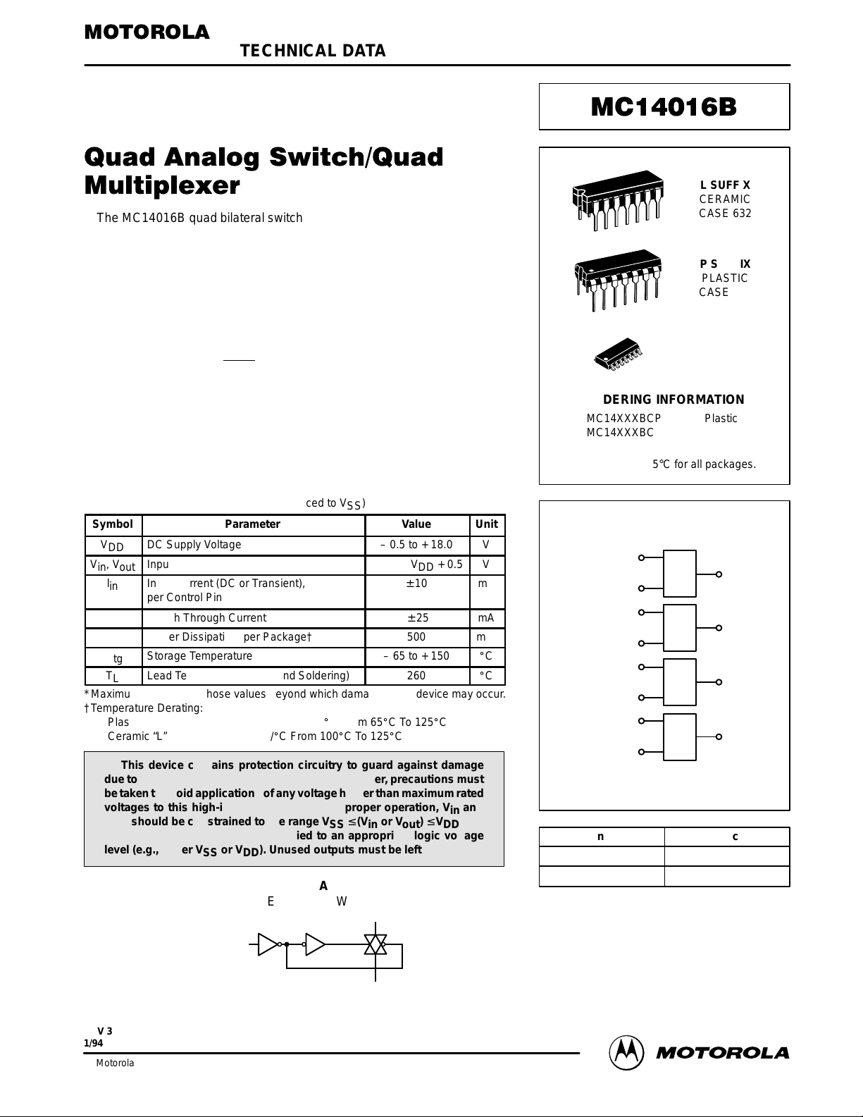
L SUFFIX
CERAMIC
CASE 632
ORDERING INFORMATION
MC14XXXBCP Plastic
MC14XXXBCL Ceramic
MC14XXXBD SOIC
TA = – 55° to 125°C for all packages.
P SUFFIX
PLASTIC
CASE 646
D SUFFIX
SOIC
CASE 751A
BLOCK DIAGRAM
CONTROL 1
IN 1
CONTROL 2
IN 2
CONTROL 3
IN 3
CONTROL 4
IN 4
OUT 1
OUT 2
OUT 3
OUT 4
13
1
5
4
6
8
12
11
2
3
9
10
VDD = PIN 14
VSS = PIN 7
Control Switch
0 = V
SS
Off
1 = V
DD
On
LOGIC DIAGRAM
(1/4 OF DEVICE SHOWN)
CONTROL
OUT
IN
LOGIC DIAGRAM RESTRICTIONS
VSS
≤
Vin ≤ V
DD
VSS
≤
V
out
≤ V
DD
Page 2
MOTOROLA CMOS LOGIC DATAMC14016B
66
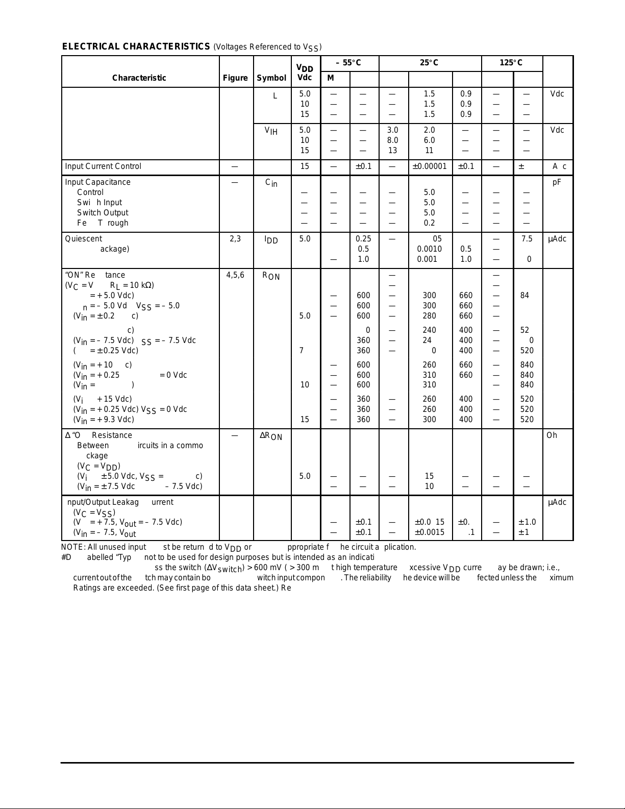
ELECTRICAL CHARACTERISTICS (Voltages Referenced to V
SS
)
V
– 55_C
25_C
125_C
Characteristic
Figure
Symbol
V
DD
Vdc
Min
Max
Min
ÎÎÎ
ÎÎÎ
ÎÎÎ
Typ #
Max
Min
Max
Unit
V
IL
5.0
10
15
—
—
—
—
—
—
—
—
—
ÎÎÎ
ÎÎÎ
ÎÎÎ
ÎÎÎ
1.5
1.5
1.5
0.9
0.9
0.9
—
—
—
—
—
—
Vdc
V
IH
5.0
10
15
—
—
—
—
—
—
3.0
8.0
13
ÎÎÎ
ÎÎÎ
ÎÎÎ
ÎÎÎ
ÎÎÎ
2.0
6.0
11
—
—
—
—
—
—
—
—
—
Vdc
Input Current Control
—
I
in
15
—
±0.1
—
ÎÎÎ
ÎÎÎ
ÎÎÎ
±0.00001
±0.1
—
± 1.0
µAdc
Input Capacitance
Control
Switch Input
Switch Output
Feed Through
—
C
in
—
—
—
—
—
—
—
—
—
—
—
—
—
—
—
—
ÎÎÎ
ÎÎÎ
ÎÎÎ
ÎÎÎ
ÎÎÎ
5.0
5.0
5.0
0.2
—
—
—
—
—
—
—
—
—
—
—
—
pF
Quiescent Current
(Per Package)
2,3
I
DD
5.0
10
15
—
—
—
0.25
0.5
1.0
—
—
—
ÎÎÎ
ÎÎÎ
ÎÎÎ
ÎÎÎ
ÎÎÎ
0.0005
0.0010
0.0015
0.25
0.5
1.0
—
—
—
7.5
15
30
µAdc
“ON” Resistance
(VC = VDD, RL = 10 kΩ)
(Vin = + 5.0 Vdc)
(Vin = – 5.0 Vdc) VSS = – 5.0 Vdc
(Vin = ± 0.25 Vdc)
4,5,6
R
ON
5.0
—
—
—
600
600
600
—
—
—
—
—
ÎÎÎ
ÎÎÎ
ÎÎÎ
ÎÎÎ
ÎÎÎ
300
300
280
660
660
660
—
—
—
—
—
840
840
840
Ohms
(Vin = + 7.5 Vdc)
(Vin = – 7.5 Vdc) VSS = – 7.5 Vdc
(Vin = ± 0.25 Vdc)
7.5
—
—
—
360
360
360
—
—
—
ÎÎÎ
ÎÎÎ
ÎÎÎ
ÎÎÎ
240
240
180
400
400
400
—
—
—
520
520
520
(Vin = + 10 Vdc)
(Vin = + 0.25 Vdc) VSS = 0 Vdc
(Vin = + 5.6 Vdc)
10
—
—
—
600
600
600
—
—
—
ÎÎÎ
ÎÎÎ
ÎÎÎ
ÎÎÎ
ÎÎÎ
260
310
310
660
660
660
—
—
—
840
840
840
(Vin = + 15 Vdc)
(Vin = + 0.25 Vdc) VSS = 0 Vdc
(Vin = + 9.3 Vdc)
15
—
—
—
360
360
360
—
—
—
ÎÎÎ
ÎÎÎ
ÎÎÎ
ÎÎÎ
260
260
300
400
400
400
—
—
—
520
520
520
∆ “ON” Resistance
Between any 2 circuits in a common
package
(VC = VDD)
(Vin = ± 5.0 Vdc, VSS = – 5.0 Vdc)
(Vin = ± 7.5 Vdc, VSS = – 7.5 Vdc)
—
∆R
ON
5.0
7.5——
—
—
—
—
ÎÎÎ
ÎÎÎ
ÎÎÎ
ÎÎÎ
ÎÎÎ
ÎÎÎ
15
10
—
—
—
—
—
—
Ohms
Input/Output Leakage Current
(VC = VSS)
(Vin = + 7.5, V
out
= – 7.5 Vdc)
(Vin = – 7.5, V
out
= + 7.5 Vdc)
—
—
7.5
7.5——
±0.1
±0.1——
ÎÎÎ
ÎÎÎ
ÎÎÎ
ÎÎÎ
ÎÎÎ
±0.0015
±0.0015
±0.1
± 0.1——
± 1.0
± 1.0
µAdc
NOTE: All unused inputs must be returned to VDD or VSS as appropriate for the circuit application.
#Data labelled “Typ” is not to be used for design purposes but is intended as an indication of the IC’s potential performance.
**For voltage drops across the switch (∆V
switch
) > 600 mV ( > 300 mV at high temperature), excessive VDD current may be drawn; i.e., the
current out of the switch may contain both VDD and switch input components. The reliability of the device will be unaffected unless the Maximum
Ratings are exceeded. (See first page of this data sheet.) Reference Figure 14.
Input Voltage
Control Input
1
Page 3
MOTOROLA CMOS LOGIC DATA
67
MC14016B
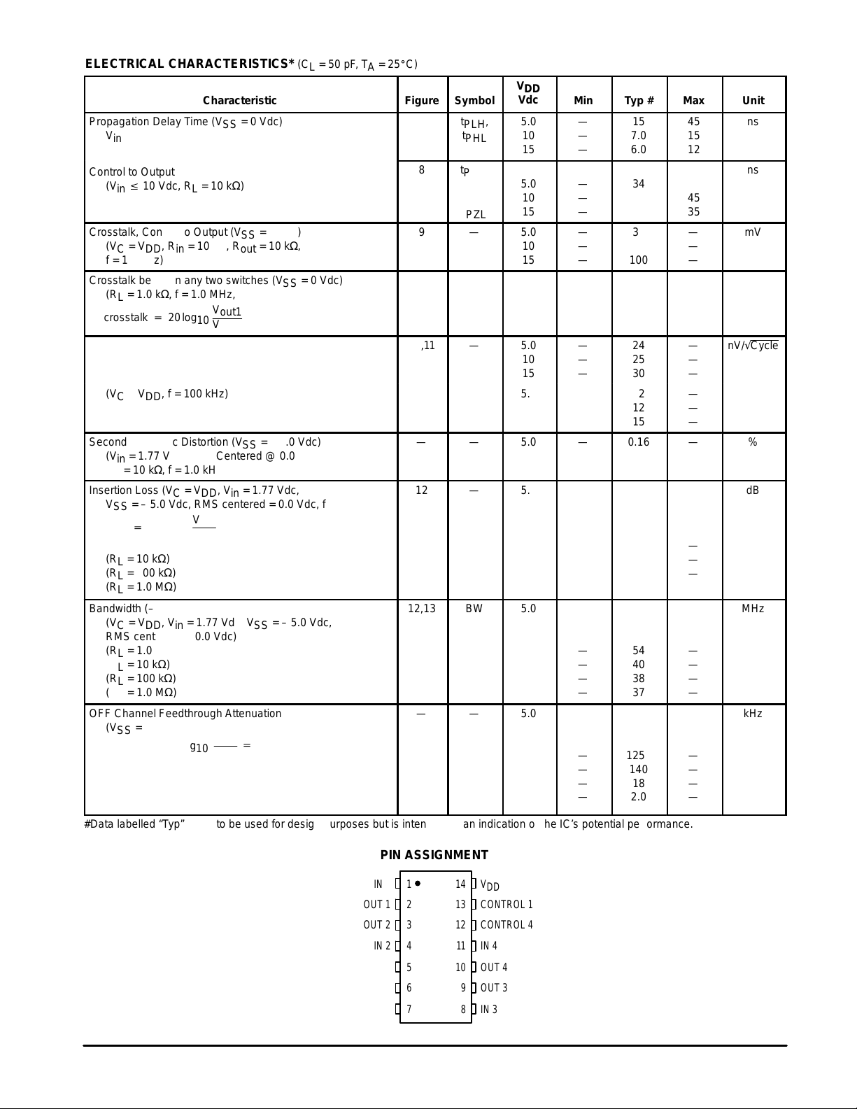
ELECTRICAL CHARACTERISTICS* (C
L
= 50 pF, TA = 25_C)
Characteristic
Figure
Symbol
V
DD
Vdc
Min
Typ #
ÎÎÎ
ÎÎÎ
ÎÎÎ
ÎÎÎ
Max
Unit
7
t
PLH
,
t
PHL
5.0
10
15
—
—
—
15
7.0
6.0
ÎÎÎ
ÎÎÎ
ÎÎÎ
ÎÎÎ
45
15
12
ns
v
10 Vdc, RL = 10 kΩ)
8
t
PHZ
,
t
PLZ
,
t
PZH
,
t
PZL
5.0
10
15
—
—
—
34
20
15
ÎÎÎ
ÎÎÎ
ÎÎÎ
ÎÎÎ
ÎÎÎ
90
45
35
ns
Crosstalk, Control to Output (VSS = 0 Vdc)
(VC = VDD, Rin = 10 kΩ, R
out
= 10 kΩ,
f = 1.0 kHz)
9
—
5.0
10
15
—
—
—
30
50
100
ÎÎÎ
ÎÎÎ
ÎÎÎ
ÎÎÎ
—
—
—
mV
Crosstalk between any two switches (VSS = 0 Vdc)
(RL = 1.0 kΩ, f = 1.0 MHz,
crosstalk+20log
10
V
out1
V
out2
)
—
—
5.0
—
– 80
ÎÎÎ
ÎÎÎ
ÎÎÎ
ÎÎÎ
ÎÎÎ
—
dB
Noise Voltage (VSS = 0 Vdc)
(VC = VDD, f = 100 Hz)
10,11
—
5.0
10
15
—
—
—
24
25
30
ÎÎÎ
ÎÎÎ
ÎÎÎ
ÎÎÎ
—
—
—
nV/√Cycle
(VC = VDD, f = 100 kHz)
5.0
10
15
—
—
—
12
12
15
ÎÎÎ
ÎÎÎ
ÎÎÎ
ÎÎÎ
ÎÎÎ
—
—
—
Second Harmonic Distortion (VSS = – 5.0 Vdc)
(Vin = 1.77 Vdc, RMS Centered @ 0.0 Vdc,
RL = 10 kΩ, f = 1.0 kHz)
—
—
5.0
—
0.16
ÎÎÎ
ÎÎÎ
ÎÎÎ
ÎÎÎ
—
%
Insertion Loss (VC = VDD, Vin = 1.77 Vdc,
VSS = – 5.0 Vdc, RMS centered = 0.0 Vdc, f = 1.0 MHz)
I
loss
+
20log
10
V
out
V
in
)
(RL = 1.0 kΩ)
(RL = 10 kΩ)
(RL = 100 kΩ)
(RL = 1.0 MΩ)
12
—
5.0
—
—
—
—
2.3
0.2
0.1
0.05
ÎÎÎ
ÎÎÎ
ÎÎÎ
ÎÎÎ
ÎÎÎ
ÎÎÎ
ÎÎÎ
—
—
—
—
dB
Bandwidth (– 3.0 dB)
(VC = VDD, Vin = 1.77 Vdc, VSS = – 5.0 Vdc,
RMS centered @ 0.0 Vdc)
(RL = 1.0 kΩ)
(RL = 10 kΩ)
(RL = 100 kΩ)
(RL = 1.0 MΩ)
12,13
BW
5.0
—
—
—
—
54
40
38
37
ÎÎÎ
ÎÎÎ
ÎÎÎ
ÎÎÎ
ÎÎÎ
ÎÎÎ
ÎÎÎ
—
—
—
—
MHz
OFF Channel Feedthrough Attenuation
(VSS = – 5.0 Vdc)
V
out
V
in
+
–50dB)
(RL = 1.0 kΩ)
(RL = 10 kΩ)
(RL = 100 kΩ)
(RL = 1.0 MΩ)
(VC = VSS, 20 log
10
—
—
5.0
—
—
—
—
1250
140
18
2.0
ÎÎÎ
ÎÎÎ
ÎÎÎ
ÎÎÎ
ÎÎÎ
ÎÎÎ
ÎÎÎ
—
—
—
—
kHz
#Data labelled “Typ” is not to be used for design purposes but is intended as an indication of the IC’s potential performance.
PIN ASSIGNMENT
11
12
13
14
8
9
105
4
3
2
1
7
6
OUT 4
IN 4
CONTROL 4
CONTROL 1
V
DD
IN 3
OUT 3
IN 2
OUT 2
OUT 1
IN 1
V
SS
CONTROL 3
CONTROL 2
Propagation Delay Time (VSS = 0 Vdc)
Vin to V
out
(VC = VDD, RL = 10 kΩ)
Control to Output
(Vin
Page 4

MOTOROLA CMOS LOGIC DATAMC14016B
68
Figure 1. Input Voltage Test Circuit
V
C
V
in
V
out
I
S
VIL: VC is raised from VSS until VC = VIL.
VIL: at VC = VIL: IS = ±10 µA with Vin = VSS, V
out
= VDD or Vin = VDD, V
out
= VSS.
VIH: When VC = VIH to VDD, the switch is ON and the RON specifications are met.
Figure 2. Quiescent Power Dissipation
Test Circuit
Figure 3. Typical Power Dissipation per Circuit
(1/4 of device shown)
PULSE
GENERATOR
V
DD
10 k
I
D
V
DDVout
V
SS
V
in
f
c
TO ALL
4 CIRCUITS
PD = VDD x I
D
50 M10 M1.0 M100 k10 k5.0 k
10,000
1000
100
10
1.0
TA = 25
°
C
10 Vdc
5.0 Vdc
fc, FREQUENCY (Hz)
, POWER DISSIPATION (P
D
µ
W)
CONTROL
INPUT
VDD = 15 Vdc
TYPICAL RON versus INPUT VOLTAGE
Figure 4. VSS = – 5.0 V and – 7.5 V Figure 5. VSS = 0 V
, “ON” RESISTANCE (OHMS)R
ON
700
600
500
400
300
200
100
0
–10 –8.0 –4.0 0 4.0 8.0 10
Vin, INPUT VOLTAGE (Vdc)
, “ON” RESISTANCE (OHMS)R
ON
700
600
500
400
300
200
100
0
0 2.0 6.0 10 14 18 20
Vin, INPUT VOLTAGE (Vdc)
RL = 10 k
Ω
TA = 25°C
VC = VDD = 5.0 Vdc
VSS = –5.0 Vdc
VC = VDD = 7.5 Vdc
VSS = –7.5 Vdc
VSS = 0 Vdc
RL = 10 k
Ω
TA = 25°C
VC = VDD = 10 Vdc
VC = VDD = 15 Vdc
Page 5

MOTOROLA CMOS LOGIC DATA
69
MC14016B
Figure 6. RON Characteristics
Test Circuit
Figure 7. Propagation Delay Test Circuit
and Waveforms
V
C
V
in
V
out
R
L
V
out
V
in
RLC
L
20 ns 20 ns
V
DD
V
SS
V
in
V
out
t
PLH
t
PHL
50%
10%
50%
90%
Figure 8. Turn–On Delay Time Test Circuit
and Waveforms
Figure 9. Crosstalk Test Circuit
V
C
V
out
V
in
R
L
C
L
V
X
20 ns
V
C
V
out
V
out
10%
90%
10%
90%
90%
50%
10%
t
PZH
t
PHZ
V
DD
V
SS
t
PLZ
t
PZL
Vin = V
DD
Vx = V
SS
Vin = V
SS
Vx = V
DD
V
C
V
out
V
in
1 k
10 k 15 pF
Figure 10. Noise Voltage Test Circuit Figure 11. Typical Noise Characteristics
VC = V
DD
OUT
IN
QUAN–TECH
MODEL
2283
OR EQUIV
100 k10 k1.0k10010
35
30
25
20
0
10 Vdc
5.0 Vdc
f, FREQUENCY (Hz)
NOISE VOLTAGE (nV/ CYCLE)
15
10
5.0
VDD = 15 Vdc
Page 6

MOTOROLA CMOS LOGIC DATAMC14016B
70
Figure 12. Typical Insertion Loss/Bandwidth
Characteristics
Figure 13. Frequency Response Test Circuit
V
C
V
out
R
L
V
in
+ 2.5 Vdc
0.0 Vdc
– 2.5 Vdc
100 M10 M1.0 M100 k10 k
2.0
0
–2.0
RL = 1 MΩ AND 100 k
Ω
fin, INPUT FREQUENCY (Hz)
–4.0
–6.0
–8.0
–10
–12
TYPICAL INSERTION LOSS (dB)
10 k
Ω
1.0 k
Ω
–3.0 dB (RL = 1.0 MΩ )
–3.0 dB (RL = 10 kΩ )
–3.0 dB (RL = 1.0 kΩ )
Figure 14. ∆V Across Switch
CONTROL
SECTION
OF IC
SOURCE
V
LOAD
ON SWITCH
Page 7

MOTOROLA CMOS LOGIC DATA
71
MC14016B
APPLICATIONS INFORMATION
Figure A illustrates use of the Analog Switch. The 0–to–5 V
Digital Control signal is used to directly control a 5 V
p–p
ana-
log signal.
The digital control logic levels are determined by VDD and
VSS. The VDD voltage is the logic high voltage; the VSS voltage is logic low. For the example, VDD = +5 V logic high at
the control inputs; VSS = GND = 0 V logic low.
The maximum analog signal level is determined by V
DD
and VSS. The analog voltage must not swing higher than
VDD or lower than VSS.
The example shows a 5 V
p–p
signal which allows no
margin at either peak. If voltage transients above VDD and/or
below VSS are anticipated on the analog channels, external
diodes (Dx) are recommended as shown in Figure B. These
diodes should be small signal types able to a bsorb t he
maximum anticipated current surges during clipping.
The
absolute
maximum potential difference between V
DD
and VSS is 18.0 V . Most parameters are specified up to 15 V
which is t he
recommended
maximum d ifference between
VDD and VSS.
Figure A. Application Example
+5 V
V
DD
V
SS
SWITCH
IN
SWITCH
OUT
5 V
p–p
ANALOG SIGNAL
0–TO–5 V DIGITAL
CONTROL SIGNALS
+5 V
EXTERNAL
CMOS
DIGITAL
CIRCUITRY
5 V
p–p
ANALOG SIGNAL
MC14016B
+5.0 V
+2.5 V
GND
Figure B. External Germanium or Schottky Clipping Diodes
V
DD
V
DD
D
x
D
x
D
x
D
x
V
SS
V
SS
SWITCH
IN
SWITCH
OUT
Page 8

MOTOROLA CMOS LOGIC DATAMC14016B
72
OUTLINE DIMENSIONS
L SUFFIX
CERAMIC DIP PACKAGE
CASE 632–08
ISSUE Y
DIM MIN MAX MIN MAX
MILLIMETERSINCHES
A 0.750 0.785 19.05 19.94
B 0.245 0.280 6.23 7.11
C 0.155 0.200 3.94 5.08
D 0.015 0.020 0.39 0.50
F 0.055 0.065 1.40 1.65
G 0.100 BSC 2.54 BSC
J 0.008 0.015 0.21 0.38
K 0.125 0.170 3.18 4.31
L 0.300 BSC 7.62 BSC
M 0 15 0 15
N 0.020 0.040 0.51 1.01
____
NOTES:
1. DIMENSIONING AND TOLERANCING PER ANSI
Y14.5M, 1982.
2. CONTROLLING DIMENSION: INCH.
3. DIMENSION L TO CENTER OF LEAD WHEN
FORMED PARALLEL.
4. DIMENSION F MAY NARROW TO 0.76 (0.030)
WHERE THE LEAD ENTERS THE CERAMIC
BODY.
–A–
–B–
C
14 PLD
GF N
K
14 PLJ
M
L
S
B
M
0.25 (0.010) T
S
A
M
0.25 (0.010) T
–T–
SEATING
PLANE
1 7
14 9
P SUFFIX
PLASTIC DIP PACKAGE
CASE 646–06
ISSUE L
NOTES:
1. LEADS WITHIN 0.13 (0.005) RADIUS OF TRUE
POSITION AT SEATING PLANE AT MAXIMUM
MATERIAL CONDITION.
2. DIMENSION L TO CENTER OF LEADS WHEN
FORMED PARALLEL.
3. DIMENSION B DOES NOT INCLUDE MOLD
FLASH.
4. ROUNDED CORNERS OPTIONAL.
1 7
14 8
B
A
F
H G D
K
C
N
L
J
M
SEATING
PLANE
DIM MIN MAX MIN MAX
MILLIMETERSINCHES
A 0.715 0.770 18.16 19.56
B 0.240 0.260 6.10 6.60
C 0.145 0.185 3.69 4.69
D 0.015 0.021 0.38 0.53
F 0.040 0.070 1.02 1.78
G 0.100 BSC 2.54 BSC
H 0.052 0.095 1.32 2.41
J 0.008 0.015 0.20 0.38
K 0.115 0.135 2.92 3.43
L 0.300 BSC 7.62 BSC
M 0 10 0 10
N 0.015 0.039 0.39 1.01
_ _ _ _
Page 9

MOTOROLA CMOS LOGIC DATA
73
MC14016B
OUTLINE DIMENSIONS
D SUFFIX
PLASTIC SOIC PACKAGE
CASE 751A–03
ISSUE F
NOTES:
1. DIMENSIONING AND TOLERANCING PER ANSI
Y14.5M, 1982.
2. CONTROLLING DIMENSION: MILLIMETER.
3. DIMENSIONS A AND B DO NOT INCLUDE
MOLD PROTRUSION.
4. MAXIMUM MOLD PROTRUSION 0.15 (0.006)
PER SIDE.
5. DIMENSION D DOES NOT INCLUDE DAMBAR
PROTRUSION. ALLOWABLE DAMBAR
PROTRUSION SHALL BE 0.127 (0.005) TOTAL
IN EXCESS OF THE D DIMENSION AT
MAXIMUM MATERIAL CONDITION.
–A–
–B–
G
P
7 PL
14 8
71
M
0.25 (0.010) B
M
S
B
M
0.25 (0.010) A
S
T
–T–
F
R
X 45
SEATING
PLANE
D 14 PL
K
C
J
M
_
DIM MIN MAX MIN MAX
INCHESMILLIMETERS
A 8.55 8.75 0.337 0.344
B 3.80 4.00 0.150 0.157
C 1.35 1.75 0.054 0.068
D 0.35 0.49 0.014 0.019
F 0.40 1.25 0.016 0.049
G 1.27 BSC 0.050 BSC
J 0.19 0.25 0.008 0.009
K 0.10 0.25 0.004 0.009
M 0 7 0 7
P 5.80 6.20 0.228 0.244
R 0.25 0.50 0.010 0.019
_ _ _ _
How to reach us:
USA/EUROPE/Locations Not Listed: Motorola Literature Distribution; JAPAN: Nippon Motorola Ltd.; Tatsumi–SPD–JLDC, 6F Seibu–Butsuryu–Center,
P.O. Box 20912; Phoenix, Arizona 85036. 1–800–441–2447 or 602–303–5454 3–14–2 Tatsumi Koto–Ku, Tokyo 135, Japan. 03–81–3521–8315
MFAX: RMFAX0@email.sps.mot.com – TOUCHTONE 602–244–6609 ASIA/PACIFIC: Motorola Semiconductors H.K. Ltd.; 8B Tai Ping Industrial Park,
INTERNET: http://Design–NET.com 51 Ting Kok Road, Tai Po, N.T., Hong Kong. 852–26629298
Motorola reserves the right to make changes without further notice to any products herein. Motorola makes no warranty , representation or guarantee regarding
the suitability of its products for any particular purpose, nor does Motorola assume any liability arising out of the application or use of any product or circuit,
and specifically disclaims any and all liability, including without limitation consequential or incidental damages. “Typical” parameters which may be provided
in Motorola data sheets and/or specifications can and do vary in different applications and actual performance may vary over time. All operating parameters,
including “Typicals” must be validated for each customer application by customer’s technical experts. Motorola does not convey any license under its patent
rights nor the rights of others. Motorola products are not designed, intended, or authorized for use as components in systems intended for surgical implant
into the body, or other applications intended to support or sustain life, or for any other application in which the failure of the Motorola product could create a
situation where personal injury or death may occur. Should Buyer purchase or use Motorola products for any such unintended or unauthorized application,
Buyer shall indemnify and hold Motorola and its officers, employees, subsidiaries, affiliates, and distributors harmless against all claims, costs, damages, and
expenses, and reasonable attorney fees arising out of, directly or indirectly, any claim of personal injury or death associated with such unintended or
unauthorized use, even if such claim alleges that Motorola was negligent regarding the design or manufacture of the part. Motorola and are registered
trademarks of Motorola, Inc. Motorola, Inc. is an Equal Opportunity/Affirmative Action Employer .
MC14016B/D
*MC14016B/D*
◊
 Loading...