

Page 1
Device
Operating
Temperature Range
Package
SEMICONDUCTOR
TECHNICAL DATA
TV HORIZONTAL
PROCESSOR
ORDERING INFORMATION
MC1391P TA = 0° to +70°C Plastic DIP
Order this document by MC1391/D
P SUFFIX
PLASTIC PACKAGE
CASE 626
8
1
1
MOTOROLA ANALOG IC DEVICE DATA
The MC1391 provides low–level horizontal sections including phase
detector, oscillator and pre–driver. This device was designed for use in all
types of television receivers.
• Internal Shunt Regulator
• Preset Hold Control Capability
• ±300 Hz Typical Pull–In
• Linear Balanced Phase Detector
• Variable Output Duty Cycle for Driving Tube or Transistor
• Low Thermal Frequency Drift
• Small Static Phase Error
• Adjustable DC Loop Gain
• Positive Flyback Inputs
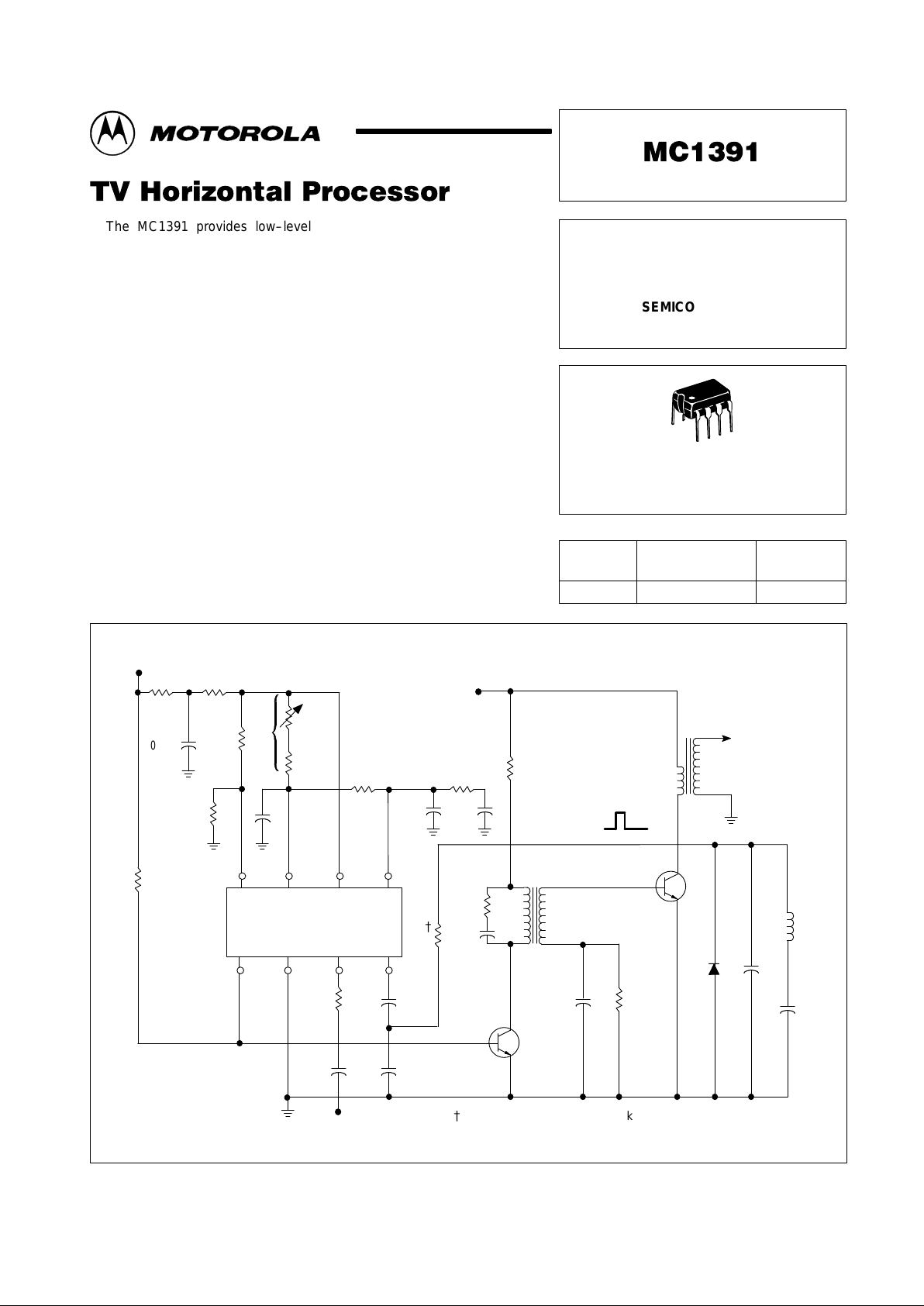
Figure 1. Simplified Application
–20V Sync
MC1391P
2.2kR
F
To
High
Voltage
Tripler
Y
O
K
E
MRD
1140
or
Equiv
1.5
5.0
µ
F
MPS–U04
or Equiv
4k
10W
C
C
+
1
µ
F
150k
Ry
R
x
3.3k
C
B
15.3:1
15k
2143
39k
0.1
µ
F
R
Z
{
82k
+150V
3k
Hold
12k
R
C
R
D
2.7k
+
C
A
100
µ
F
R
E
2.4k
5768
MJ105 or Equiv
R
A
R
B
V
nonreg
+ 30V
470 470
0.0068
µ
F
0.005
µ
F
0.01
µ
F
0.2
µ
F
0.1
µ
F
0.003
µ
F
This circuit has an oscillator pull–in range of
±
300 Hz, a noise bandwidth of 320 Hz, and a damping factor of 0.8.
{
RZ = 6.8 k per 100 V of flyback amplitude.
0.001
µ
F
Motorola, Inc. 1996 Rev 2
Page 2
MC1391
2
MOTOROLA ANALOG IC DEVICE DATA
MAXIMUM RATINGS
(TA = +25°C, unless otherwise noted.)
Rating
Value Unit
Supply Current 40 mAdc
Output Voltage 40 Vdc
Output Current 30 mAdc
Sync Input Voltage (Pin 3) 5.0 V
pp
Flyback Input Voltage (Pin 4) 5.0 V
pp
Power Dissipation (Package Limitation)
Plastic Package
Derate above TA = +25°C
625
5.0
mW
mW/°C
Operating T emperature Range (Ambient) 0 to +70 °C
Storage Temperature Range –65 to +150 °C
ELECTRICAL CHARACTERISTICS (T
A
= +25°C, unless otherwise noted. See Test Circuit of Figure 2, all switches in position 1.)
Characteristics
Min Typ Max Unit
Regulated Voltage (Pin 6) 8.0 8.6 9.4 Vdc
Supply Current (Pin 6) – 20 – mAdc
Collector–Emitter Saturation Voltage (Output Transistor Q1 in Figure 6)
(IC = 20 mA, Pin 1 ) Vdc
– 0.15 0.25
Vdc
Voltage (Pin 4) – 2.0 – Vdc
Oscillator Pull–in Range (Adjust RH in Figure 2) – ±300 – Hz
Oscillator Hold–in Range (Adjust RH in Figure 2) – ±900 – Hz
Static Phase Error
(∆f = 300 Hz)
– 0.5 –
µs
Free–running Frequency Supply Dependance
(S1 in position 2)
– ±3.0 –
Hz/Vdc
Phase Detector Leakage (Pin 5)
(All switches in position 2)
– – ±1.0
µA
Sync Input Voltage (Pin 3) 2.0 – 5.0 V
pp
Sawtooth Input Voltage (Pin 4) 1.0 – 3.0 V
pp
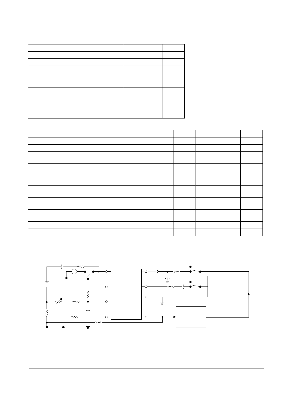
Figure 2. Test Circuit
MC1391P
Output
Pulse
+30V
1
2
3
4
39k
1
2
2
S2
S3
0.1
µ
F
5
6
7
8
S1
1
150k
3.3k
+
–
2
+4.0V
12k
3.0k
R
H
1.0k
1.0k
2.0k
6800pF
V
M
VCC +30V
Pulse Generator
Output = +50 V
12
µ
s
Pulse Generator
Sync Pulse =
–20 V , 5.0
µ
s,
fO = 15.750 Hz
1
0.1µF
0.003
µ
F
µ
A
(See Figure 5)
0.1
µ
F
+
3.3k
Page 3

MC1391
3
MOTOROLA ANALOG IC DEVICE DATA
Figure 3. Frequency versus Temperature Figure 4. Frequency Drift versus Warm–Up Time
Figure 5. Mark Space Ratio
Figure 6. Representative Schematic Diagram
TA, AMBIENT TEMPERATURE (°C)
01020304050607080
f, FREQUENCY (Hz)
Reference Frequency
= 15.750 Hz
S3 in Position 2
t, TIME (s)
0306090120
f, FREQUENCY DRIFT (Hz)
∆
Reference Frequency
= 15.750Hz
POSITIVE PULSE WIDTH (µs)
01020304050
V , VOLTAGE (V)
M
fO = 15,750 Hz
t = 63.5
µ
s
R22
Oscillator Regulator
6
V
CC
Oscillator
Timing
7
Pre–Driver Phase Detector
Z2
R14
330
R11
3.0k
Z1
D1
D2
D3
D4
R8
2.4k
R6
3.3k
Q6
2.6kR1
Mark–Space
8
Ratio
R17
10k
2.15
Q18
R23
2k
5
Phase
Detector
Output
Q7 Q8
R9
1.2k
Q10
Q9
470
R7
Q13
R
18
Q15
Q16
4
Sawtooth
Input
Q14
k
7.5k
R19
Q12 Q17
R20
510
R21
910
R
16
6.8k
3
Sync Input
2
Ground
Q2
Q1
Q4
Q5
R4 430
2.4kR5
7.5kR3
R12
820
R15
3.3k
R10
3.6k
R13
240
6.8kR2
Q3
1
Output
7.5k
Q11
30
20
10
0
–10
–20
–30
–40
–50
–60
–70
40
30
10
0
20
4.75
4.5
4.25
3.75
3.5
3.25
3.0
2.75
4.0
Page 4

MC1391
4
MOTOROLA ANALOG IC DEVICE DATA
CIRCUIT OPERA TION
The MC1391P contains the oscillator, phas e detector and
predriver sections needed for a television horizontal APC loop.
The oscillator is an RC type with one pin (Pin 7) used to
control the timing. The basic operation can be explained
easily. If it is assumed that Q7 is initially of f, then the capacitor
connected from Pin 7 to ground will be charged by an
external resistor (RC) connected to Pin 6. As soon as the
voltage at Pin 7 exceeds the potential set at the base of Q8
by resistors R8 and R10, Q7 will turn on and Q6 will supply
base current to Q5 and Q10. Transistor Q10 will set a new,
lower potential at the base of Q8 determined by R8, R9 and
R10. At the same time, transistor Q5 will discharge the
capacitor through R4 until the base bias of Q7 falls below that
of Q8, at which time Q7 will turn off and the cycle repeats.
The sawtooth generated at the base of Q4 will appear
across R3 and turn off Q3 whenever it exceeds the bias
set on Pin 8. By adjusting the potential at Pin 8, the duty
cycle (MSR) at the predriver output pin (Pin 1) can be
changed to accommodate either tube or transistor horizontal
output stages.
The phase detector is isolated from the remainder of the
circuit by R14 and Z2. The phase detector consists of the
comparator Q15, Q16 and the gated current source Q17.
Negative going sync pulses at Pin 3 turn off Q12 and the
current division between Q15 and Q16 will be determined by
the phase relationship of the sync and the sawtooth
waveform at Pin 4, which is derived from the horizontal
flyback pulse. If there is no phase difference between the
sync and sawtooth, equal currents will flow in the collectors of
Q15 and Q16 each of half the sync pulse period. The current
in Q15 is turned around by Q18 so that there is no net output
current at Pin 5 for balanced conditions. When a phase offset
occurs, current will flow either in or out of Pin 5. This pin is
connected via an external low–pass filter to Pin 7, thus
controlling the oscillator.
Shunt regulation for the circuit is obtained with a zero
temperature coefficient from the series combination of D1,
D2 and Z1.
APPLICATION INFORMATION
Although it is an integrated circuit, the MC1391P has all
the flexibility of a conventional discrete component horizontal
APC loop. The internal temperature compensated voltage
regulator allows a wide supply voltage variation to be
tolerated, enabling operation from nonregulated power
supplies. A minimum value for supply current into Pin 6 to
maintain zener regulation is about 18 mA. Allowing 2.0 mA for
the external dividers
RA + RB =
V
nonreg(min)
–8.8
20 x 10
–3
Components RA, RB and CA are used for ripple rejection. If
the supply voltage ripple is expected to be less than 100 mV
(for a 30 V supply) then RA and RB can be combined and
CA omitted.
The output pulse width can be varied from 6.0 µs to 48 µs
by changing the voltage at Pin 8 (see Figure 5). However,
care should be taken to keep the lead lengths to Pin 8 as
short as possible at Pin 1. The parallel impedance of RD and
RE should be close to 1.0 kΩ to ensure stable pulse widths.
For 15 mA drive at saturation
15 x 10
–3
V
nonreg
–0.3
RF =
The oscillator free–running frequency is set by RC and C
B
connected to Pin 7. For values of RC ≥ R
discharge
(R4 in
Figure 6), a useful approximation for the free–running
frequency is
fO =
1
0.6 RCC
B
Proper choice of RC and CB will give a wide range of
oscillator frequencies – operation at 31.5 kHz for countdown
circuits is possible for example. As long as the product RCC
B
≈ 10–4 many combinations of values of RC and CB will satisfy
the free–running frequency requirement of 15.734 kHz.
However, the sensitivity of the oscillator (β) to control–current
from the phase detector is directly dependent on the
magnitude of RC, and this provides a convenient method of
adjusting the dc loop gain (fc).
For a given phase detector sensitivity (µ) = 1.6 0 x 1 0–4 A/rad
fc = µβ and β = 3.15 x RC Hz/mA
Increasing RC will raise the dc loop gain and reduce the static
phase error (S.P.E.) for a given frequency offset. Secondary
effects are to increas e the natural resonant frequency of the
loop (ωn) and give a wider pull–in range from an out–of–loc k
condition. The loop will also tend to be underdamped with fast
pull–in times, producing good airplane flutter performance.
However, as the loop becomes more underdamped impulse
noise can cause shock excitation of the loop. Unlimited
increase in the dc loop gain will also rais e the noise bandwidth
excessively causing horizontal jitter with thermal noise. Once
the dc loop gain has been selected for adequate SPE
performance, the loop filter can be used to produce the balance
between other desirable characteristics. Damping of the loop is
achieved most directly by changing the resistor RX with respect
to RY which modifies the ac/dc gain ration (m) of the loop.
Lowering this ratio will reduce the pull–in range and noise
bandwidth (fnn). (Note: very large values of RY will limit the
control capability of the phase detector with a corresponding
reduction in hold–in range.)
Static phasing can be adjusted simply by adding a small
resistor between the flyback pulse integrating capacitor and
ground. The sync coupling capacitor should not be too small
or it can charge during the vertical pulse and this may result in
picture bends at the top of the CRT.
Note: In adjusting the loop parameters, the following
equations may prove useful:
(1 + c )T
1 x χ2 Tω
C
fnn =
4 χ T
ω
C
wn =
K =
χ
2Tω
C
4
R
X
RY
χ =
ωC = 2 π
fc
T = Ry CC
where: K = loop damping coeffecient
√
Page 5

MC1391
5
MOTOROLA ANALOG IC DEVICE DATA
OUTLINE DIMENSIONS
NOTES:
1. DIMENSION L TO CENTER OF LEAD WHEN
FORMED PARALLEL.
2. PACKAGE CONTOUR OPTIONAL (ROUND OR
SQUARE CORNERS).
3. DIMENSIONING AND TOLERANCING PER ANSI
Y14.5M, 1982.
14
58
F
NOTE 2
–A–
–B–
–T–
SEATING
PLANE
H
J
G
D
K
N
C
L
M
M
A
M
0.13 (0.005) B
M
T
DIM MIN MAX MIN MAX
INCHESMILLIMETERS
A 9.40 10.16 0.370 0.400
B 6.10 6.60 0.240 0.260
C 3.94 4.45 0.155 0.175
D 0.38 0.51 0.015 0.020
F 1.02 1.78 0.040 0.070
G 2.54 BSC 0.100 BSC
H 0.76 1.27 0.030 0.050
J 0.20 0.30 0.008 0.012
K 2.92 3.43 0.115 0.135
L 7.62 BSC 0.300 BSC
M ––– 10 ––– 10
N 0.76 1.01 0.030 0.040
__
P SUFFIX
PLASTIC PACKAGE
CASE 626–05
ISSUE K
Page 6

MC1391
6
MOTOROLA ANALOG IC DEVICE DATA
Motorola reserves the right to make changes without further notice to any products herein. Motorola makes no warranty , representation or guarantee regarding
the suitability of its products for any particular purpose, nor does Motorola assume any liability arising out of the application or use of any product or circuit, and
specifically disclaims any and all liability, including without limitation consequential or incidental damages. “T ypical” parameters which may be provided in Motorola
data sheets and/or specifications can and do vary in different applications and actual performance may vary over time. All operating parameters, including “Typicals”
must be validated for each customer application by customer’s technical experts. Motorola does not convey any license under its patent rights nor the rights of
others. Motorola products are not designed, intended, or authorized for use as components in systems intended for surgical implant into the body, or other
applications intended to support or sustain life, or for any other application in which the failure of the Motorola product could create a situation where personal injury
or death may occur. Should Buyer purchase or use Motorola products for any such unintended or unauthorized application, Buyer shall indemnify and hold Motorola
and its officers, employees, subsidiaries, affiliates, and distributors harmless against all claims, costs, damages, and expenses, and reasonable attorney fees
arising out of, directly or indirectly, any claim of personal injury or death associated with such unintended or unauthorized use, even if such claim alleges that Motorola
was negligent regarding the design or manufacture of the part. Motorola and are registered trademarks of Motorola, Inc. Motorola, Inc. is an Equal
Opportunity/Affirmative Action Employer.
How to reach us:
USA/EUROPE/ Locations Not Listed: Motorola Literature Distribution; JAPAN: Nippon Motorola Ltd.; Tatsumi–SPD–JLDC, 6F Seibu–Butsuryu–Center,
P.O. Box 20912; Phoenix, Arizona 85036. 1–800–441–2447 or 602–303–5454 3–14–2 Ta tsumi Koto–Ku, Tokyo 135, Japan. 03–81–3521–8315
MFAX: RMF AX0@email.sps.mot.com – TOUCHT ONE 602–244–6609 ASIA/PACIFIC: Motorola Semiconductors H.K. Ltd.; 8B Tai Ping Industrial Park,
INTERNET: http://Design–NET.com 51 Ting Ko k Road, Tai Po, N.T ., Hong Kong. 852–26629298
MC1391/D
*MC1391/D*
◊
 Loading...