

Page 1
Order this document by MC1378/D
The MC1378 is a bipolar composite video overlay encoder and
microcomputer synchronizer. The MC1378 contains the complete encoder
function of the MC1377, i.e., quadrature color modulators, RGB matrix, and
blanking level clamps, plus a complete complement of synchronizers to lock
a microcomputer–based video source to any remote video source. The
MC1378 can be used as a local system timing and encoding source, but it is
most valuable when used to lock the microcomputer source to a remotely
originated video signal.
• Contains All Needed Reference Oscillators
• Can Be Operated in PAL or NTSC Mode, 625 or 525 Line
• Wideband, Full–Fidelity Color Encoding
• Local or Remote Modes of Operation
• Minimal External Components
• Designed to Operate from 5.0 V supply
• Will Work with non standard Video
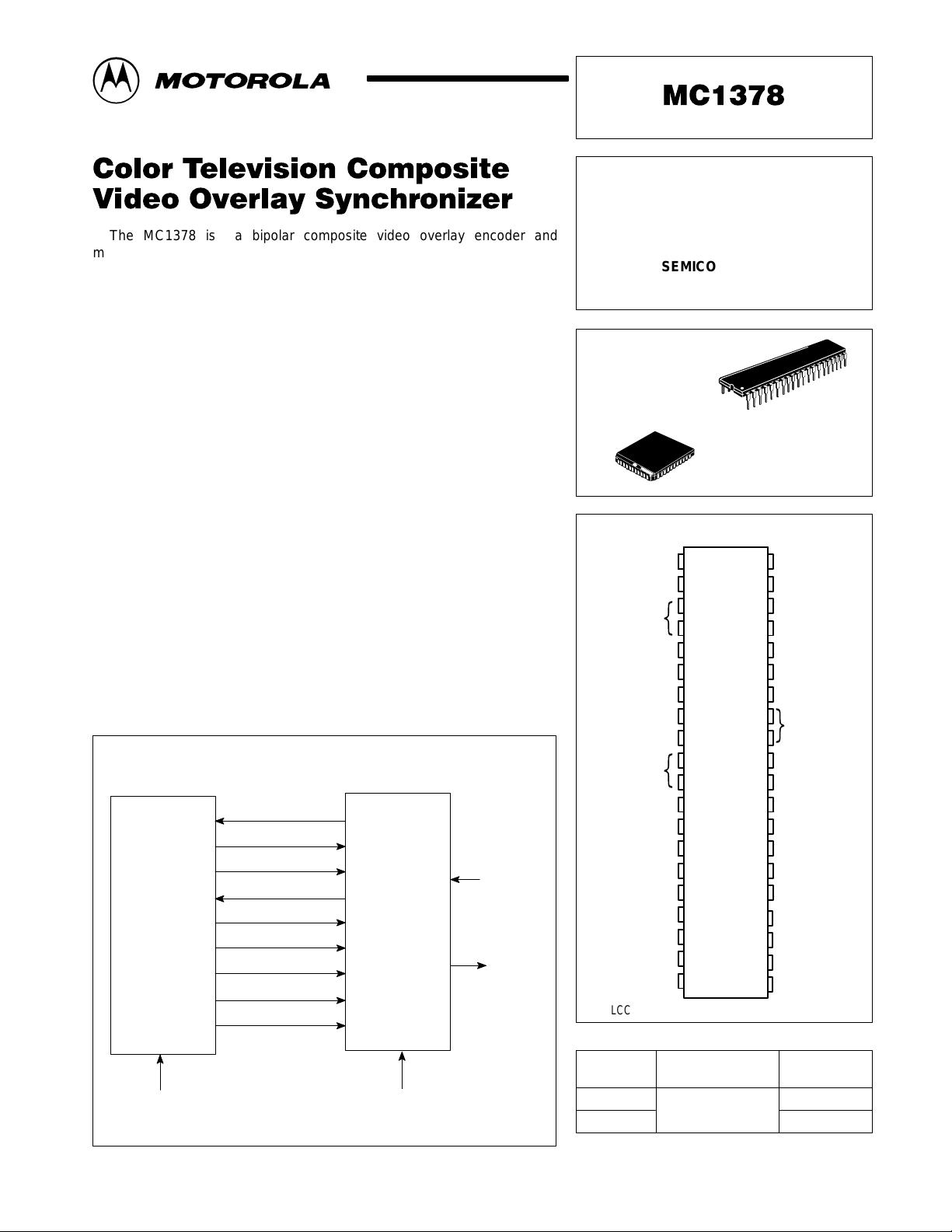
Figure 1. Simplified Application
36MHz Master Clock
H Sync
Video
System
525/60
625/50
3.58/4.43MHz
Vert/Comp Sync
Red
Green
Blue
Video Enable
Local/Remote
MC1378
PAL/
NTSC
Remote
Video
Composite
Overplayed
Video
COLOR TELEVISION
COMPOSITE VIDEO OVERLAY
SYNCHRONIZER
SEMICONDUCTOR
TECHNICAL DATA
P SUFFIX
PLASTIC PACKAGE
CASE 711
40
1
FN SUFFIX
PLASTIC PACKAGE
1
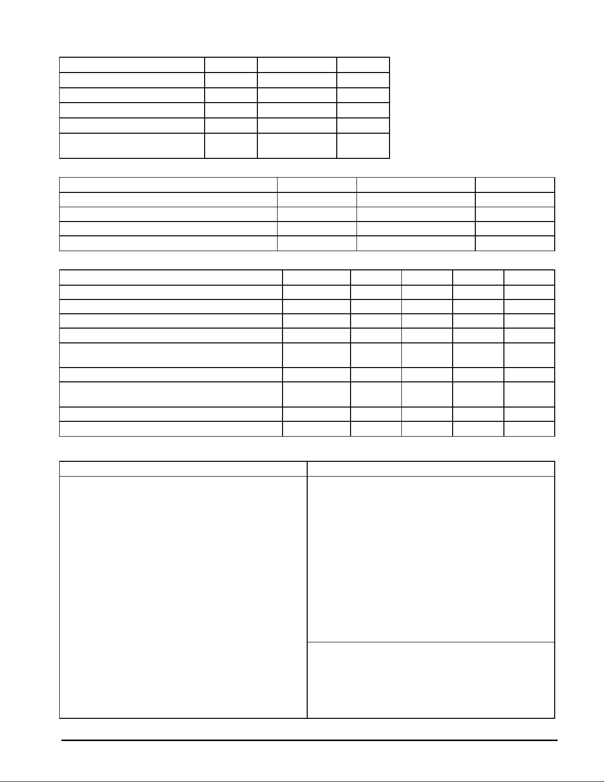
PIN CONNECTIONS
Local/Rem.
H. PLL Filter
H. VCO
Burst Gate Out
PAL/NTSC Mode
Ground
3.58/4.43 In
Chroma PLL Filter
Chroma VCO
R–Y Clamp
B–Y Clamp
R Input
G Input
B Input
–Y Output
Chroma Out
Loc. Vid. Clamp
Chroma In
* ( ) PLCC Pin Assignments
{
{
1 (1)
2 (2)
3 (3)
4 (4)
5 (5)
6 (7)
7 (8)
8 (9)
9 (10)
10 (11)
11 (12)
12 (13)
13 (14)
14 (15)
15 (16)
16 (18)
17 (19)
18 (20)
19 (21)
20 (22)
ORDERING INFORMATION
Operating
Device
MC1378P
MC1378FN
Temperature Range
TA = 0° to +70°C
CASE 777
(PLCC–44)
(44) 40
(43) 39
(42) 38
(41) 37
(40) 36
(38) 35
(37) 34
(36) 33
(35) 32
(34) 31
(33) 30
(32) 29
(31) 28
(30) 27
(29) 26
(27) 25
(26) 24
(25) 23
(24) 22
(23) 21
H. Sync In
Comp. Sync Out
V. Out/Sync In
Clock PLL Filter
Clock V
CC
Clock Output
Clock Ground
Clock VCO
}
Killer Filter
Quad. Loop Filter
PAL Indent. Cap
V
CC
Comp. Vid. Out
Ground
Overlay Enable
Rem. Vid. In
ACC Filter
–Y Input
Rem. Vid. Clamp
Package
Plastic DIP
PLCC–44
MOTOROLA ANALOG IC DEVICE DATA
Motorola, Inc. 1996 Rev 0
1
Page 2
MC1378
MAXIMUM RATINGS
Rating Symbol Value Unit
Supply Voltage V
Operating Temperature T
Storage Temperature T
Junction Temperature T
Power Dissipation, Package
Derate above 25°C
CC
A
stg
J(max)
P
D
RECOMMENDED OPERATING CONDITIONS
Condition Pin Value Unit
Supply Voltage 28, 36 5.4 ± 0.25 Vdc
RGB Input for 100% Saturation 14, 15, 16 1.0 Vpp
Color Oscillator Input Level 8 0.5 Vpp
Video Input, Positive 24 1.0 Vpp
6.0 Vdc
0 to +70 °C
–65 to +150 °C
150 °C
1.25
10
W
mW/°C
ELECTRICAL CHARACTERISTICS (V
Characteristics
Supply Current 28, 36 – 100 – mAdc
Video Output, Open Circuit, Positive 27 – 2.0 9.4 V
Modulation Angle (R – Y) to (B – Y) – 87 90 93 Degrees
RGB Input Impedance 14, 15, 16 – 10 – kΩ
Local/Remote Switch (TTL) High
Horizontal Sync Input, Negative Going (TTL) 40 – 4.3 – V
Vertical Sync Output, Negative Going,
Remote Mode (TTL)
Composite Sync Output, Negative Going (TTL) 39 – 4.3 – V
Burst Gate Output, Positive Going (TTL) 5 – 4.3 – V
= 5.0 V, TA = 25°C, circuit of Figure 4 or 5)
CC
Pin Min Typ Max Unit
Low
1 – Remote
38 – 4.3 – V
pp
– –
Local
pp
pp
pp
pp
Description of Operation – Refer to Figures 3, 4
Remote Mode Local Mode
The incoming remote video signal (Pin 24) supplies all
synchronizing information. A discussion of the function of the
phase detectors helps to clarify the lockup method:
PD1 locks the internally counted–down 4 MHz horizontal VCO
to the incoming horizontal sync. It is fast acting, to follow
VCR source fluctuations.
PD2 locks the 36 MHz clock VCO, which is divided down by
the video system, to the divided down horizontal VCO.
PD3 is a gated phase detector which locks the 14 MHz crystal
oscillator, divided by 4, to the incoming color burst.
PD4 controls an internal phase shifter to assure that the
outgoing color burst is the same phase as incoming burst
at PD3.
PD5 not used in REMOTE MODE
Vertical lock is obtained by continuously resetting the sync
generator in the video system with separated vertical sync from the
MC1378, Pin 38. This signal is TTL level vertical block sync,
negative going. The horizontal sync from the video system to Pin 40
is also TTL level with sync negative going. The local/remote switch,
Pin 1, is in local mode when grounded, remote mode when taken
to 5.0 V . The overlay control, Pin 25, has an analog characteristic,
centered about 1.0 V , which allows fading from local to remote.
The MC1378 and a video system combine to provide a fully
synchronized standard signal source. In this case, composite sync
must be supplied by the video system or other time base system.
In the MC1378 the phase detectors operate as follows:
PD1 locks the internally counted–down 4 MHz horizontal VCO
to a Horizontal Sync signal (at Pin 40) from the video
system (counted down from 36 MHz)
PD2 not used in LOCAL MODE.
PD3 not used in LOCAL MODE.
PD4 active, but providing an arbitrary phase shift setting
between the color oscillator and the output burst phase.
PD5 locks the 36 MHz clock VCO (which is divided down by
the video system) to the 14 MHz (crystal) color oscillator.
The 14 MHz is, therefore, the system standard in LOCAL
MODE, and is not DC controlled.
COMPOSITE VIDEO GENERATION
The color encoding at the RGB signals is done exactly as in
the MC1377. Composite chroma is looped out at Pins 18 and 20
to allow the designer to choose band shaping. Luminance is
similarly brought out (Pins 17 and 22) to permit installation of
the appropriate delay.
Composite sync output, Pin 39, and burst gate output, Pin 5,
are provided for convenience only.
2
MOTOROLA ANALOG IC DEVICE DATA
Page 3

Figure 2.
+5.0 V
MC1378
4 MHz
Cer
Res
H Sync In
Comp
4
3
2
28
VCO
HORIZ
Divide by 256 Counter
H
PD2
PD1
PD3PD4
BG
40
L
R
Sync Out
39
L
Kill
Proc
Kill
Det
1
R
Local/Remote
Loc/Rem
Proc
Ident
Det
Ident
38
Switches
L
Vert. Out
Comp. Sync In
R
Vert
BG
L Clamp Video
Sync Sep
Video
Clamp
Remote
Fast
Video
Switch
Comp
Sync Sep
7/26
212429312725192318202217
Enable
Overlay
Gnd
Remote
Video
Out
Video In
CC
V
Burst Gate Out
Figure 2. Representative Block Diagram
MHz In
35.8/4.43
Out
Clock
36 35 37 8 30 5
34
CC
V
Clock
+5.0 V
Burst
Burst
R
Clock
33
Flag
Flag
PD5
VCO
BG
Decoder
BR
Decoder
L
32
R
9
F/F
PAL
ACC DET
H/2
Phase
90–270
Shift
R–YB–Y
Cont
PAL/NTSC
6
Mod Mod
R–Y
Clamp
B – Y
Clamp
B–Y
Diff
Color
12
13
14
15
Shift
Phase
0 – 180
Divide by 4 Ring Counter
L
VCO
4XSC
11
10
and
R–Y
Luma
16
Matrix
Local
Video
L
Clamp
Ref
V
R
ACC
AMP
Chroma
In Chroma In
–Y
–Y
Out
Out
Gnd
Clock
35.8/
35.5
MHz
MOTOROLA ANALOG IC DEVICE DATA
17.73
14.32/
MHz
PAL/
NTSC
RGB
In
3
Page 4

÷
2275
÷
2270
Local
Video
Source
H Sync
Local/
Remote
(High)
R
G
B
Overlay Enable
Master Clock 35.8/35.5MHz
V. Sync
Comp
Sync
Out
0.033
+
47k 47
12
1.8k
1.0
3456 78910111213141516 181920
4
680
MHz
Cer
+
0.022
Res
15
Burst
Gate
Out
1.0µF
MC1378
Figure 3. Remote Mode
36MHz
Clock
0.3
0.001
µ
0.001
H
36pF
2.2
0.01
k
1.0µF
0.047
PAL
0.001
NTSC
0.1 0.1
470k
17.73 MHz
+
20pF
14.32/
+ 5
V
CC
10
+
0.0047
0.10.1
0.1
Video
Out
µ
F
75
10
µ
F10 µF
Remote
Video
In
++ +
10
µ
F
1.0µF
17
100/62
µ
F
TOKO
220
+++
10
166NNF
10264AG
1.0
µ
F
21232425272829303132333353637383940 26 224
1.2k
TDK
SDL–4301
1.2k
0.001
3.3k
+
1.0
µ
47/33
F
Local
Video
Source
÷
÷
2275
2270
÷
10
÷
8
Overlay Enable
Master Clock 35.8/35.5MHz
Composite Sync
Comp
Sync
Out
H Sync
12
Local/
1.8k
Remote
(High)
1.0
+
0.022
R
G
B
Figure 4. Local Mode
+ 5
Video
V
Out
36MHz
0.047
Clock
0.001
0.001
0.3
µ
0.1 0.1
H
470k
0.033
1.0µF
+
47k 47
36pF
3 4 5 6 78 9 10 111213141516 1819 20
4
680
MHz
PAL
Cer
NTSC
Res
15
Burst
Gate
Out
0.001
2.2
0.01
k
17.73MHz
+
20pF
14.32/
CC
+
0.0047
0.1
0.10.1
75
10
µ
F10 µF
17
100/62
+++
10
µ
F
TOKO
166NNF
10264AG
++
1.0µF
21232425272829303132333353637383940 26 224
220
3.3k
+
1.0
µ
F
1.0
0.001
µ
F
47/33
1.2k
1.2k
TDK
SDL–4301
4
MOTOROLA ANALOG IC DEVICE DATA
Page 5

OUTLINE DIMENSIONS
40 21
1 20
A
DFGH
–N–
D
BRK
Y
MC1378
P SUFFIX
PLASTIC PACKAGE
CASE 711–03
ISSUE C
B
C
N
K
SEATING
PLANE
FN SUFFIX
PLASTIC PACKAGE
CASE 777–02
(PLCC–44)
ISSUE C
M
NOTES:
1. POSITIONAL TOLERANCE OF LEADS (D), SHALL
BE WITHIN 0.25 (0.010) AT MAXIMUM MATERIAL
CONDITION, IN RELATION TO SEATING PLANE
AND EACH OTHER.
2. DIMENSION L TO CENTER OF LEADS WHEN
FORMED PARALLEL.
3. DIMENSION B DOES NOT INCLUDE MOLD FLASH.
M
L–M
T
S
L–M
INCHESMILLIMETERS
S
S
S
DIM MIN MAX MIN MAX
A 51.69 52.45 2.035 2.065
B 13.72 14.22 0.540 0.560
L
J
B
C 3.94 5.08 0.155 0.200
D 0.36 0.56 0.014 0.022
F 1.02 1.52 0.040 0.060
G 2.54 BSC 0.100 BSC
H 1.65 2.16 0.065 0.085
J 0.20 0.38 0.008 0.015
K 2.92 3.43 0.115 0.135
L 15.24 BSC 0.600 BSC
M 0 15 0 15
__ __
N 0.51 1.02 0.020 0.040
0.007(0.180) N
U
M
T
0.007(0.180) N
–L–
A
R
Z
C
G
G1
0.010 (0.25) N
S
T
NOTES:
1. DATUMS –L–, –M–, AND –N– ARE DETERMINED
WHERE TOP OF LEAD SHOULDER EXITS PLASTIC
BODY AT MOLD PARTING LINE.
2. DIMENSION G1, TRUE POSITION TO BE MEASURED
AT DATUM –T–, SEATING PLANE.
3. DIMENSIONS R AND U DO NOT INCLUDE MOLD
FLASH. ALLOWABLE MOLD FLASH IS 0.010 (0.25) PER
SIDE.
4. DIMENSIONING AND TOLERANCING PER ANSI
Y14.5M, 1982.
5. CONTROLLING DIMENSION: INCH.
6. THE PACKAGE TOP MAY BE SMALLER THAN THE
PACKAGE BOTTOM BY UP TO 0.012 (0.300).
DIMENSIONS R AND U ARE DETERMINED AT THE
OUTERMOST EXTREMES OF THE PLASTIC BODY
EXCLUSIVE OF MOLD FLASH, TIE BAR BURRS, GATE
BURRS AND INTERLEAD FLASH, BUT INCLUDING
ANY MISMATCH BETWEEN THE TOP AND BOTTOM
OF THE PLASTIC BODY.
7. DIMENSION H DOES NOT INCLUDE DAMBAR
PROTRUSION OR INTRUSION. THE DAMBAR
PROTRUSION(S) SHALL NOT CAUSE THE H
DIMENSION TO BE GREATER THAN 0.037 (0.940).
THE DAMBAR INTRUSION(S) SHALL NOT CAUSE THE
H DIMENSION TO BE SMALLER THAN 0.025
144
V
L–M
–M–
Z
D
W
X
VIEW D–D
0.007(0.180) N
0.007(0.180) N
M
M
S
L–M
T
L–M
T
S
S
S
H
J
E
0.004 (0.10)
SEATING
–T–
PLANE
S
VIEW S
S
K
G1
S
0.010 (0.25) N
0.007(0.180) N
L–M
T
M
L–M
T
K1
F
0.007(0.180) N
M
S
L–M
T
S
S
S
S
S
VIEW S
MILLIMETERSINCHES
0.635
DIM MIN MAX MIN MAX
A 0.685 0.695 17.40 17.65
B 0.685 0.695 17.40 17.65
C 0.165 0.180 4.20 4.57
E 0.090 0.110 2.29 2.79
F 0.013 0.019 0.33 0.48
G 0.050 BSC 1.27 BSC
H 0.026 0.032 0.66 0.81
J 0.020 ––– 0.51 –––
K 0.025 ––– 0.64 –––
R 0.650 0.656 16.51 16.66
U 0.650 0.656 16.51 16.66
V 0.042 0.048 1.07 1.21
W 0.042 0.048 1.07 1.21
X 0.042 0.056 1.07 1.42
Y ––– 0.020 ––– 0.50
Z 2 10 2 10
____
G1 0.610 0.630 15.50 16.00
.
K1 0.040 ––– 1.02 –––
MOTOROLA ANALOG IC DEVICE DATA
5
Page 6

MC1378
Motorola reserves the right to make changes without further notice to any products herein. Motorola makes no warranty , representation or guarantee regarding
the suitability of its products for any particular purpose, nor does Motorola assume any liability arising out of the application or use of any product or circuit, and
specifically disclaims any and all liability, including without limitation consequential or incidental damages. “T ypical” parameters which may be provided in Motorola
data sheets and/or specifications can and do vary in different applications and actual performance may vary over time. All operating parameters, including “Typicals”
must be validated for each customer application by customer’s technical experts. Motorola does not convey any license under its patent rights nor the rights of
others. Motorola products are not designed, intended, or authorized for use as components in systems intended for surgical implant into the body, or other
applications intended to support or sustain life, or for any other application in which the failure of the Motorola product could create a situation where personal injury
or death may occur. Should Buyer purchase or use Motorola products for any such unintended or unauthorized application, Buyer shall indemnify and hold Motorola
and its officers, employees, subsidiaries, affiliates, and distributors harmless against all claims, costs, damages, and expenses, and reasonable attorney fees
arising out of, directly or indirectly, any claim of personal injury or death associated with such unintended or unauthorized use, even if such claim alleges that Motorola
was negligent regarding the design or manufacture of the part. Motorola and are registered trademarks of Motorola, Inc. Motorola, Inc. is an Equal
Opportunity/Affirmative Action Employer.
How to reach us:
USA/EUROPE/Locations Not Listed: Motorola Literature Distribution; JAPAN: Nippon Motorola Ltd.; Tatsumi–SPD–JLDC, 6F Seibu–Butsuryu–Center,
P.O. Box 20912; Phoenix, Arizona 85036. 1–800–441–2447 or 602–303–5454 3–14–2 Tatsumi Koto–Ku, Tokyo 135, Japan. 03–81–3521–8315
MFAX: RMF AX0@email.sps.mot.com – TOUCHT ONE 602–244–6609 ASIA/PACIFIC: Motorola Semiconductors H.K. Ltd.; 8B Tai Ping Industrial Park,
INTERNET: http://Design–NET.com 51 Ting Kok Road, Tai Po, N.T., Hong Kong. 852–26629298
6
◊
MOTOROLA ANALOG IC DEVICE DATA
MC1378/D
*MC1378/D*
 Loading...