

Page 1
Device
Operating
Temperature Range
Package
SEMICONDUCTOR
TECHNICAL DATA
COLOR TELEVISION
RGB to PAL/NTSC ENCODER
ORDERING INFORMATION
MC1377DW
MC1377P
TA = 0° to +70°C
SO–20L
Plastic DIP
Order this document by MC1377/D
P SUFFIX
PLASTIC PACKAGE
CASE 738
DW SUFFIX
PLASTIC PACKAGE
CASE 751D
(SO–20L)
20
1
20
1
1
MOTOROLA ANALOG IC DEVICE DATA
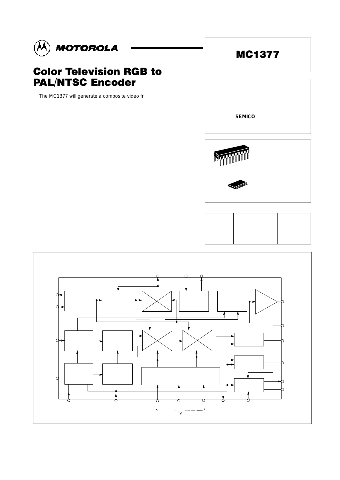
The MC1377 will generate a composite video from baseband red, green,
blue, and sync inputs. On board features include: a color subcarrier
oscillator; voltage controlled 90° phase shifter; two double sideband
suppressed carrier (DSBSC) chroma modulators; and RGB input matrices
with blanking level clamps. Such features permit system design with few
external components and accordingly, system performance comparable to
studio equipment with external components common in receiver systems.
• Self–contained or Externally Driven Reference Oscillator
• Chroma Axes, Nominally 90° (±5°), are Optionally Trimable
• PAL/NTSC Compatible
• Internal 8.2 V Regulator
Figure 1. Representative Block Diagram
Osc
out
Osc
in
NTSC/PAL
Select
Gnd
18
17
20
15
Quad
Decoup
V
CC
V
B
19 14 16
13
10
11
12
9
7
Chroma Out
Chroma In
B–Y Clamp
R–Y Clamp
Composite
Video Output
Video Clamp
1 2 3 4 5 6 8
T
rise
Composite
Sync Input
R G B
Inputs
–Y
out
–Y
in
Oscillator
Buffer
Voltage
Controlled
90
°
8.2V
Regulator
PAL
Switch
0/180
°
Chroma
Amp
B–Y
Clamp
R–Y
Clamp
Output Amp/
Clamp
Color Difference and
Luminance Matrix
Dual
Comparator
Latching
Ramp
Generator
PAL/NTSC
Control
Burst
Pulse
Driver
90
°
0
°
H/2
R–Y B–Y
R–Y B–Y
–Y
Motorola, Inc. 1995
Page 2
MC1377
2
MOTOROLA ANALOG IC DEVICE DATA
MAXIMUM OPERATING CONDITIONS
Rating Symbol Value Unit
Supply Voltage V
CC
15 Vdc
Storage Temperature T
stg
–65 to +150 °C
Power Dissipation Package
Derate above 25°C
P
D
1.25
10
W
mW/°C
Operating Temperature T
A
0 to +70 °C
RECOMMENDED OPERATING CONDITIONS
Characteristics Min Typ Max Unit
Supply Voltage 10 12 14 Vdc
IB Current (Pin 16) 0 – –10 mA
Sync, Blanking Level (DC level between pulses, see Figure 9e)
Sync Tip Level (see Figure 9e)
Sync Pulse Width (see Figure 9e)
1.7
–0.5
2.5
–
0
–
8.2
0.9
5.2
Vdc
µ
s
R, G, B Input (Amplitude)
R, G, B Peak Levels for DC Coupled Inputs, with Respect to Ground
–
2.2
1.0
–
–
4.4
V
pp
V
Chrominance Bandwidth (Non–comb Filtered Applications), (6 dB) 0.5 1.5 2.0 MHz
Ext. Subscarrier Input (to Pin 17) if On–Chip Oscillator is not used. 0.5 0.7 1.0 V
pp
ELECTRICAL CHARACTERISTICS (V
CC
= 12 Vdc, TA = 25°C, circuit of Figure 7, unless otherwise noted.)
Characteristics
Pins Symbol Min Typ Max Unit
SUPPLY CURRENT
Supply Current into V
CC,
No Load, on Pin 9. VCC = 10 V
Circuit Figure 7 VCC = 11 V
VCC = 12 V
VCC = 13 V
VCC = 14 V
14 I
CC
–
–
20
–
–
33
34
35
36
37
–
–
40
–
–
mA
VOLTAGE REGULATOR
VB Voltage (IB = –10 mA, VCC = 12 V, Figure 7)
Load Regulation (0 < IB ≤ 10 mA, VCC = 12 V)
Line Regulation (IB = 0 mA, 10 V < VCC < 14 V) ≤
16 V
B
Reg
load
Reg
line
7.7
–20
–
8.2
120
4.5
8.7
+30
–
Vdc
mV
mV/V
OSCILLATOR AND MODULATION
Oscillator Amplitude with 3.58 MHz/4.43 MHz crystal 17 Osc – 0.6 – V
pp
Subcarrier Input: Resistance at 3.58 MHz
Subcarrier Input: Resistance at 4.43 MHz
17 R
osc
–
–
5.0
4.0
–
–
kΩ
Capacitance C
osc
– 2.0 – pF
Modulation Angle (R–Y) to (B–Y)
Angle Adjustment (R–Y)
DC Bias Voltage
–
19
19
∅m
∆∅m
V
19
–
–
–
±5
0.25
6.4
–
–
–
Deg
Deg/µA
Vdc
CHROMINANCE AND LUMINANCE
Chroma Input DC Level
Chroma Input Level for 100% Saturation
10 V
in
–
–
4.0
0.7
–
–
Vdc
V
pp
Chroma Input: Resistance
Chroma Input: Capacitance
R
in
C
in
–
–
10
2.0
–
–
kΩ
pF
Chroma DC Output Level
Chroma Output Level at 100% Saturation
13 V
out
8.9
–
10
1.0
10.9
–
Vdc
V
pp
Chroma Output Resistance R
out
– 50 –
Ω
Luminance Bandwidth (–3.0 dB), Less Delay Line 9 BW
Luma
– 8.0 – MHz
Page 3
MC1377
3
MOTOROLA ANALOG IC DEVICE DATA
ELECTRICAL CHARACTERISTICS (V
CC
= 12 Vdc, TA = 25°C, circuit of Figure 7, unless otherwise noted.)
Characteristics
Pins Symbol Min Typ Max Unit
VIDEO INPUT
R, G, B Input DC Levels 3, 4, 5 RGB 2.8 3.3 3.8 Vdc
R, G, B Input for 100% Color Saturation – 1.0 – V
pp
R, G, B Input: Resistance
R, G, B Input: Capacitance
R
RGB
C
RGB
8.0
–
10
2.0
17
–
k
Ω
pF
Sync Input Resistance (1.7 V < Input < 8.2) 2
Sync
– 10 –
k
Ω
COMPOSITE VIDEO OUTPUT
Composite Output,
100% Saturation
(see Figure 8d)
Sync
Luminance
Chroma
Burst
9 CV
out
–
–
–
–
0.6
1.4
1.7
0.6
–
–
–
–
V
pp
Output Impedance (Note 1) R
video
– 50 –
Ω
Subcarrier Leakage in Output (Note 2) V
lk
– 20 – mV
pp
NOTES: 1. Output Impedance can be reduced to less than 10 Ω by using a 150 Ω output load from Pin 9 to ground. Power supply current will
increase to about 60 mA.
2.Subcarrier leakage can be reduced to less than 10 mV with optional circuitry (see Figure 12).
PIN FUNCTION DESCRIPTIONS
Symbol Pin Description
t
r
1 External components at this pin set the rise time of the internal ramp function generator (see Figure 10).
Sync
2 Composite sync input. Presents 10 kΩ resistance to input.
R 3 Red signal input. Presents 10 kΩ impedance to input. 1.0 Vpp required for 100% saturation.
G 4 Green signal input. Presents 10 kΩ impedance to input. 1.0 Vpp
required for 100% saturation.
B 5 Blue signal Input. Presents 10 kΩ impedance to input. 1.0 Vpp
required for 100% saturation.
–Y
out
6 Luma (–Y) output. Allows external setting of luma delay time.
V
clamp
7 Video Clamp pin. Typical connection is a 0.01 µF capacitor to ground.
–Y
in
8 Luma (–Y) input. Presents 10 kΩ input impedance.
CV
out
9 Composite Video output. 50 Ω output impedance.
Chroma
In
10 Chroma input. Presents 10 kΩ input impedance.
B–Y
clamp
11 B–Y clamp. Clamps B–Y during blanking with a 0.1 µF capacitor to ground.
Also used with R–Y clamp to null residual color subcarrier in output.
R–Y
clamp
12 R–Y clamp. Clamps R–Y during blanking with a 0.1 µF capacitor to ground.
Also used with B–Y clamp to null residual color subcarrier in output.
Chroma
Out
13 Chroma output. 50 Ω output impedance.
V
CC
14 Power supply pin for the IC; +12, ± 2.0 V, required at 35 mA (typical).
Gnd 15 Ground pin.
V
B
16 8.2 V reference from an internal regulator capable of delivering 10 mA to external circuitry.
Osc
in
17 Oscillator input. A transistor base presents 5.0 kΩ to an external subcarrier input, or is available for
constructing a Colpitts oscillator (see Figure 4).
Osc
out
18 Oscillator output. The emitter of the transistor, with base access at Pin 17, is accessible for completing the
Colpitts oscillator. See Figure 4.
∅
m
19 Quad decoupler. With external circuitry, R–Y to B–Y relative angle errors can be corrected. Typically,
requires a 0.01 µF capacitor to ground.
NTSC/PAL
Select
20 NTSC/PAL switch. When grounded, the MC1377 is in the NTSC mode; if unconnected, in the PAL mode.
Page 4
MC1377
4
MOTOROLA ANALOG IC DEVICE DATA
FUNCTIONAL DESCRIPTION
Figure 2. Power Supply and V
B
0.1
VCC = +12V
16
14
15
32mA
8.2V
Regulator
9
100
Figure 3. RGB Input Circuitry
13 17 18 19
Chroma
Out
Oscillator
Quad
Decoup
Amp/
Buffer
∆ Θ
PAL
Switch
0/180
°
NTSC
PAL
PAL/NTSC
Control
Burst
Flag
NTSC
PAL
B–Y R–Y
B–Y R–Y
+90
°
R
Figure 4. Chroma Section
R–Y
15µF
3
18k
B–Y –Y
RGB Matrix
18k
18k
15µF
4
G
15µF
5
B
6
–Y
27k 27k
27k
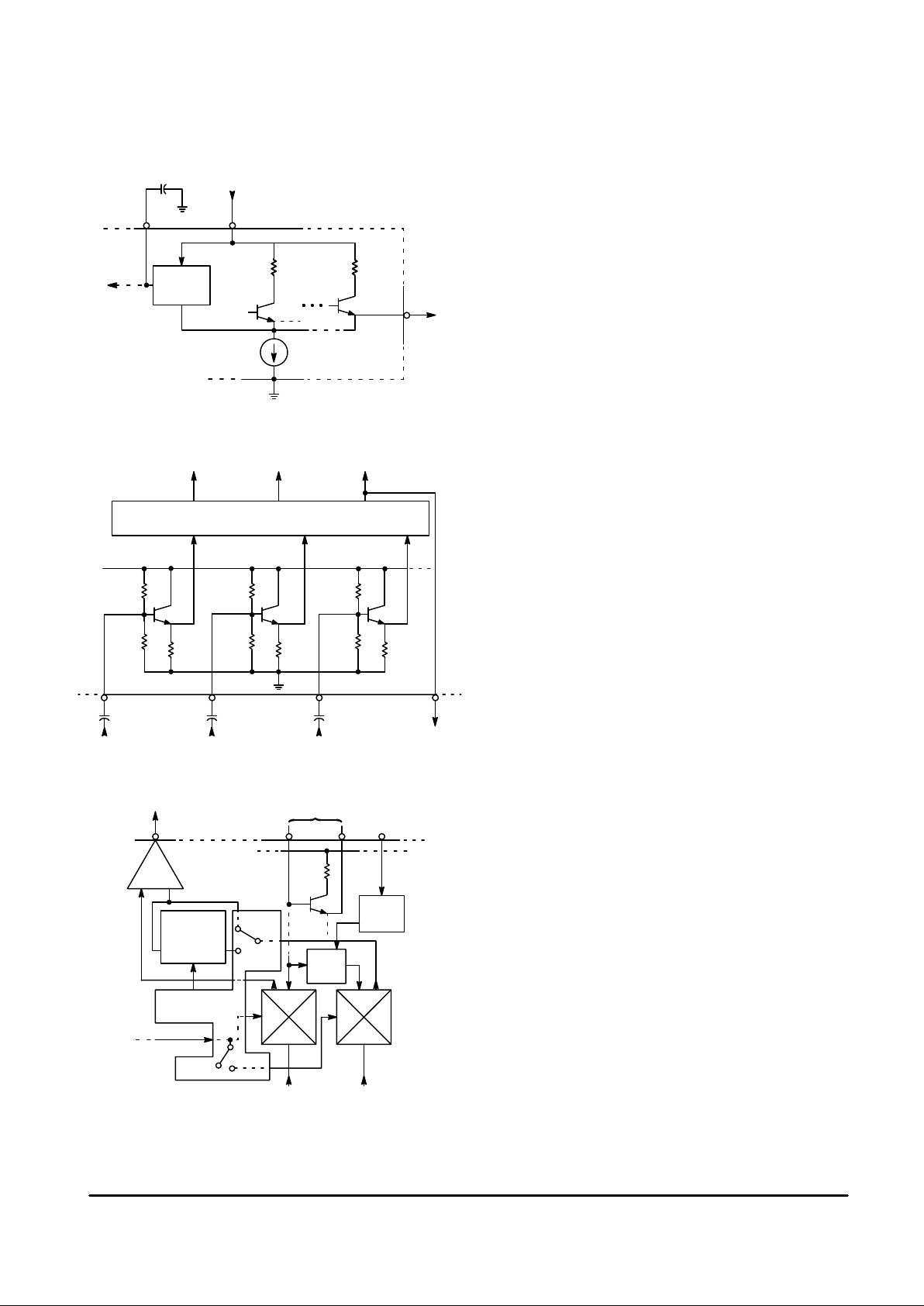
Power Supply and VB (8.2 V Regulator)
The MC1377 pin for power supply connection is Pin 14.
From the supply voltage applied to this pin, the IC biases
internal output stages and is used to power the 8.2 V internal
regulator (VB at Pin 16) which biases the majority of internal
circuitry. The regulator will provide a nominal 8.2 V and is
capable of 10 mA before degradation of performance. An
equivalent circuit of the supply and regulator is shown in
Figure 2.
R, G, B Inputs
The RGB inputs are internally biased to 3.3 V and provide
10 k
Ω of input impedance. Figure 3 shows representative
input circuitry at Pins 3, 4, and 5.
The input coupling capacitors of 15 µF are used to prevent
tilt during the 50/60 Hz vertical period. However, if it is desired
to avoid the use of the capacitors, then inputs to Pins 3, 4,
and 5 can be dc coupled provided that the signal levels are
always between 2.2 V and 4.4 V.
After input, the separate RGB information is introduced to
the matrix circuitry which outputs the R–Y, B–Y, and –Y
signals. The –Y information is routed out at Pin 6 to an
external delay line (typically 400 ns).
DSBSC Modulators and 3.58 MHz Oscillator
The R–Y and B–Y outputs (see (B–Y)/(R–Y) Axes versus
I/Q Axes, Figure 22) from the matrix circuitry are amplitude
modulated onto the 3.58/4.43 MHz subcarrier. These signals
are added and color burst is included to produce composite
chroma available at Pin 13. These functions plus others,
depending on whether NTSC or P AL operation is chosen, are
performed in the chroma section. Figure 4 shows a block
diagram of the chroma section.
The MC1377 has two double balanced mixers, and
regardless of which mode is chosen (NTSC or PAL), the
mixers always perform the same operation. The B–Y mixer
modulates the color subcarrier directly, the R–Y mixer
receives a 90
° phase shifted color subcarrier before being
modulated by the R–Y baseband information. Additional
operations are then performed on these two signals to make
them NTSC or PAL compatible.
In the NTSC mode, the NTSC/PAL control circuitry allows
an inverted burst of 3.58 MHz to be added only to the B–Y
signal. A gating pulse or “burst flag” from the timing section
permits color burst to be added to the B–Y signal. This color
burst is 180° from the B–Y signal and 90° away from the R–Y
signal (see Figure 22) and permits decoding of the color
information. These signals are then added and amplified
before being output, at Pin 13, to be bandpassed and then
reintroduced to the IC at Pin 10.
In the PAL mode, NTSC/PAL control circuitry allows an
inverted 4.43 MHz burst to be added to both R–Y and B–Y
equally to produce the characteristic PAL 225°/135 burst
phase. Also, the R–Y information is switched alternately from
180° to 0° of its original position and added to the B–Y
information to be amplified and output.
Page 5
MC1377
5
MOTOROLA ANALOG IC DEVICE DATA
Timing Circuitry
The composite sync input at Pin 2 performs three
important functions: it provides the timing (but not the
amplitude) for the sync in the final output; it drives the black
level clamps in the modulators and output amplifier; and it
triggers the ramp generator at Pin 1, which produces burst
envelope and P AL switching. A representative block diagram
of the timing circuitry is shown in Figure 5.
In order to produce a color burst, a burst envelope must be
generated which “gates” a color subcarrier into the R–Y and
B–Y modulators. This is done with the ramp generator at
Pin 1.
The ramp generator at Pin 1 is an R–C type in which the
pin is held low until the arrival of the
leading
edge of sync. The
rising ramp function, with time constant R–C, passes through
two level sensors – the first one starts the gating pulse and
the second stops it (see Figure 10). Since the “early” part of
the exponential is used, the timing provided is relatively
accurate from chip–to–chip and assembly–to–assembly.
Fixed components are usually adequate. The ramp
continues to rise for more than half of the line interval, thereby
inhibiting burst generation on “half interval” pulses on vertical
front and back porches. The ramp method will produce burst
on the vertical front and back “porches” at full line intervals.
R–Y, B–Y Clamps and Output Clamp/Amplifier
The sync signal, shown in the block diagram of Figure 6,
drives the R–Y and B–Y clamps which clamp the R–Y and
B–Y signals to reference black during the blanking periods.
The output amplifier/clamp provides this same function plus
combines and amplifies the chroma and luma components
for composite video output.
Application Circuit
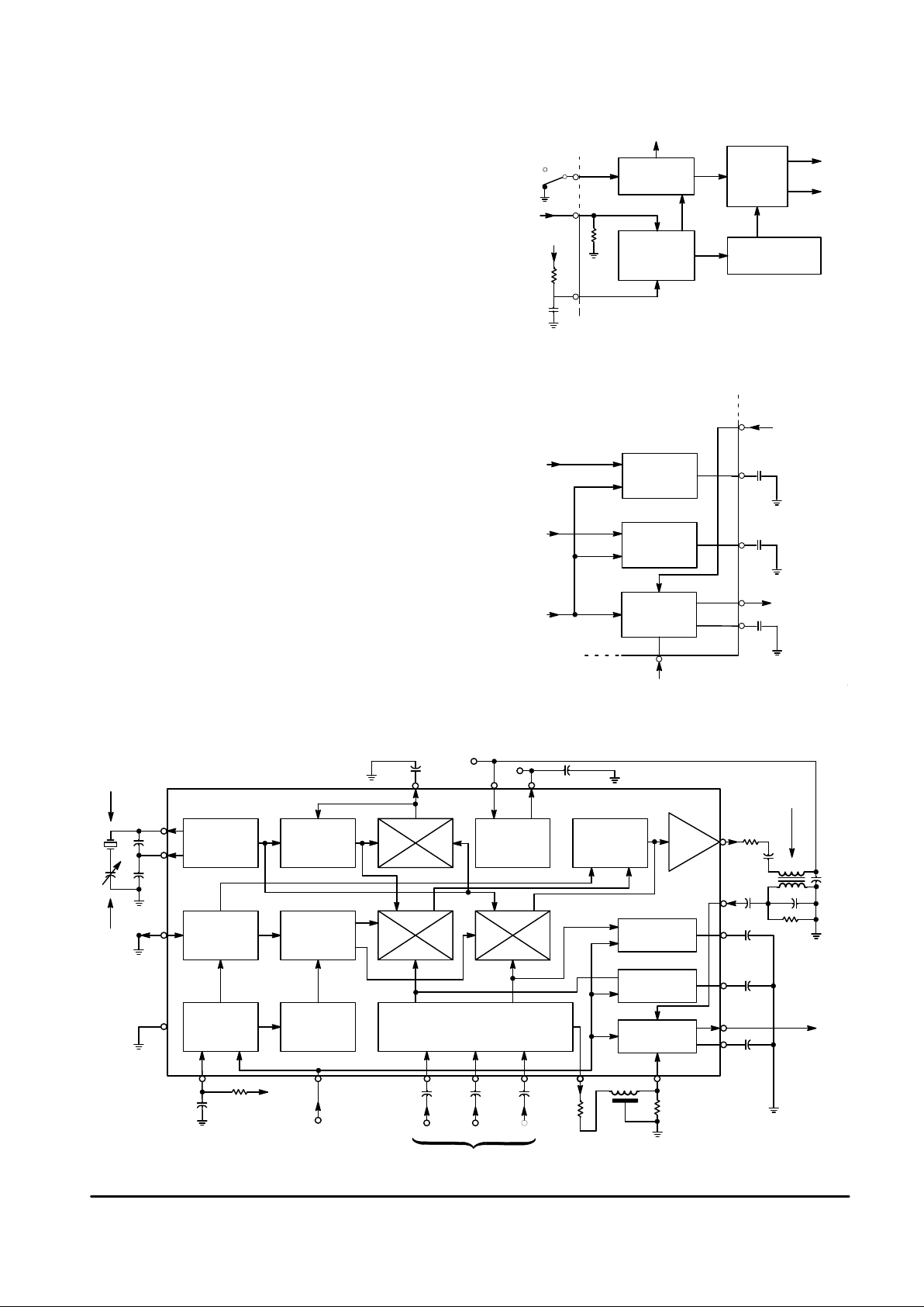
Figure 7 illustrates the block diagram of the MC1377 and
the external circuitry required for typical operation.
11
Sync
Input
Figure 5. Timing Circuitry
Figure 6. R–Y, B–Y and Output Amplifier Clamps
PAL/
NTSC
H/2
Line Drive
10k
Latching
Ramp
Generator
Dual
Comparator
Burst Flag
Burst
Pulse
Driver
PAL/NTSC
Control
20
2
1
B–Y
R–Y
Sync
B–Y
Clamp
R–Y
Clamp
Output
Amp/Clamp
Chroma
10
12
9
7
8
–Y
Composite
Video
V
B
R
C
0.1
0.1
0.01
Figure 7. Block Diagram and Application Circuit
R–Y B–Y
Osc/
Buffer
Voltage
Controlled
90
°
8.2V
Regulator
PAL
Switch
0/180
°
Chroma
Amp
B–Y
Clamp
R–Y
Clamp
Output Amp/
Clamp
Color Difference and
Luminance Matrix
Dual
Comparator
Latching
Ramp
Gen
PAL/NTS
C
Control
Burst
Pulse
Driver
0.01
19
V
CC
16
V
B
0.1
TOKO 166NNF
–10264AG
13
220
100/
62*
0.1
3.3k
47/33*
10
9
7
0.01
12
0.1
0.1
1000
3.58/
4.43*
MHz
220
220
5.0 to
25pF
20
15
1 2
3
4 5 6
8
56k
0.001
mica
Composite
Sync
Input
14
11
Composite
Video Output
1.0k
400ns
Y Delay
1.0k
+ + +
15
µ
F 15µF 15µF
V
B
R G B
R, G, B Inputs
H/2
90
°
0
°
NTSC/
PAL Select
17
18
* Refers to the choice NTSC/PAL
* (3.58 MHz/4.43 MHz).
R–Y
B–Y
–Y
–Y
Page 6

MC1377
6
MOTOROLA ANALOG IC DEVICE DATA
10k
R29
R21
220
R161
15k
R127
27k
R129
18k
R126
2.7k
R123
3.9k
T111
T23
22k
R28
R4
2.0k
+12V
+8.2V
Gnd
PAL/NTSC
Comp Sync
T
RISE
R–IN
G–IN
B–IN
R6A 5.1k
Z1
R2
1.2k
R2A
1.0k
T1
R3
6.8k
R13
22k
R11
22k
R12
10k
R14
22k
R22
270
R9
22k
560
R25
560
R26
T22
T19 T20
R23
1.5k
R24
1.5k
R18
220
R20
220
T17
T15
T16
T24 T25 T26 T27
T10
T13
R16
1.0k
R17
1.0k
T9
T8T7
R8
220
R9
220
R5
470
T5T4
+
C1
5pF
R6
5.1k
R10
5.0k
R15
T2 T3
R7
4.0k
+
C2
18pF
T11 T12
T28
5.0k
R30
R162
R71
22k
R69
R70
10k
R72
22k
R73
22k
R74
10k
R75
10k
T79
T68
T69
R77
15k
R76
15k
R80A
4.0k
R81
22k
T71
T73
T74
R83
10k
R79
1.0k
R78
15k
Z2
T75
R86
10k
T76
R87
13.8k
R88
30.4k
T77
R95
18k
T82
T81
R94
2.2k
R93
2.2k
R92
2.2k
R91
10k
T78
T79
T80
R85
10k
T72
R82
22k
R100
22k
T91B
T91A
R96
22k
R101
10k
R97
22k
R102
1.0k
T90
R99
10k
R98
22k
T92 T93
T94
R160
22k
R104
2.0k
R104
15k
R108
2.7k
R164
4.7k
T102
T103
T104
T101T100
T99T98
R107
820
T95
R105
7.5k
R110
1.0k
T105
R111
4.7k
T107
R112
36k
R113
27k
R118
R117
10k
R120
27k
T110
T109
T108
R115
18k
R119
5.3k
R116
3.9k
R122
18k
T96
R106
9.1k
R109
22k
T206
T97
191817
14
16
15
20
2
1
3
4
5
Osc In Osc Out
Quad
Decoup
10k
R121
27k
22k
R90
R80 B
6.0k
T18
T6
T14
1.5k
220
R27
220
22k
10k
Page 7

MC1377
7
MOTOROLA ANALOG IC DEVICE DATA
R31
5.1k
R31
5.1k
T30
R35
1.0k
R36
1.0k
R66
2.4k
R51
12k
R67
220
T5
4
R68
3.0k
R55
220
R54
220
T50 T51 T52 T53
T57
T56
R65
220
B–Y Clamp
T58
R58
300
R63
10k
R58
300
R60
4.7k
T59
T66
R44A
22k
R52
10k
R49
10k
R45
300
R44
22k
R43
10k
R38
10k
R47
4.7k
T45 T46
T62
T43 T44
R40
2.0k
R41
2.0K
T41T40
R47
1.0k
R46
1.0k
R39
500
T39
T47
T63
T64 T65
R62
2.0k
R61
2.0k
R56
1.0k
T55
R53
500
T49
T33 T34
T32T31
R37
220
T35 T36 T37 T38
T42
27k
R34
22k
R33
10k
R29
R21
220
R27
220
R135
220
R136
4.7k
R134
220
R133
220
R137
1.5k
R139
40k
T118
T120
R156
220
T117
470
R140
470
R141
4.7k
R138
22k
R155
20k
R144
R157
22k
R147
27k
R154
100
R153
220
T128
Composite Video Out
Video Clamp
Chroma In
R–Y Clamp
Chroma Out
–Y In
–Y Out
R151
9.1k
R149
10k
15k
R152
R150
4.7k
T126
15k
R148
10k
R142
R143
22k
R145
3.3k
T123
T124
T125
T122
T121
T119
T116
T114
R124
12.5 k
R132
1.85k
R163
10k
R125
12.5k
R131
14k
R130
3.9k
R159
10k
R127
27k
T113
T112
T127
R129
18k
R126
2.7k
R123
3.9k
T1
T23
T48
R50
220
R43A
10k
T60 T61
22k
R28
T28
5.0k
R30
T110
13
11
12
10
9
7
8
6
T115
R128
220
R158
10k
R48
500
R57
1.0k
R64
500
PAL F/F
R–Y
B–Y
Burst Flag
Burst Flag
PAL F/F
Figure 8. Internal Schematic
Page 8

MC1377
8
MOTOROLA ANALOG IC DEVICE DATA
APPLICATION INFORMATION
Figure 8. Signal Voltages
(Circuit Values of Figure 7)
4.4V
Limits
for DC
Coupled
Inputs
(a)
(b)
(c)
(d)
(e)
(f)
(g)
(h)
(i)
1.0V
pp
1.0V
pp
1.0V
pp
2.2V
5.0
4.0
3.0
8.2 Max
1.7 Min
0.9 Max
0
–0.5 Min
10.5
10.0
9.5
4.35
4.0
3.65
5.2
4.3
2.6
2.1
Luminance
Input
(Pin 8)
Luminance
Output
(Pin 6)
Chroma
Input
(Pin 10)
Chroma
Output
(Pin 13)
Sync
Input
(Pin 2)
Composite
Output
(Pin 9)
100%
Blue
Input
(Pin 5)
100%
Red
Input
(Pin 3)
100%
Green
Input
(Pin 4)
R, G, B Input Levels
The signal levels into Pins 3, 4, 5 should be 1.0 Vpp for fully
saturated, standard composite video output levels as shown
in Figure 9(d). The inputs require 1.0 Vpp since the internally
generated sync pulse and color burst are at fixed and
predetermined amplitudes.
Further, it is essential that the portion of each input which
occurs during the sync interval represent black for that input
since that level will be clamped to reference black in the color
modulators and output stage. This implies that a refinement,
such as a difference between black and blanking levels, must
be incorporated in the RGB input signals.
If Y , R–Y, B–Y and burst flag components are available and
the MC1377 is operating in NTSC, inputs may be as follows:
the Y component can be coupled through a 15 pF capacitor
to Pins 3, 4 and 5 tied together; the (–[R–Y]) component can
be coupled to Pin 12 through a 0.1 µF capacitor, and the
(–[B–Y]) and burst flag components can be coupled to Pin 1 1
in a similar manner.
Sync Input
As shown in Figure 9(e), the sync input amplitude can be
varied over a wide latitude, but will require bias pull–up from
most sync sources. The important requirements are:
1)The voltage level between sync pulses must be between
1.7 V and 8.2 V, see Figure 9(e).
2)The voltage level for the sync tips must be between
+0.9 V and – 0.5 V, to prevent substrate leakage in the IC,
see Figure 9(e).
3)The width of the sync pulse should be no longer than
5.2
µs and no shorter than 2.5 µs.
For PAL operation, correctly serrated vertical sync is
necessary to properly trigger the PAL divider. In NTSC mode,
simplified “block” vertical sync can be used but the loss of
proper horizontal timing may cause “top hook” or “flag
waving” in some monitors. An interesting note is that
composite video can be used directly as a sync signal,
provided that it meets the sync input criteria.
Latching Ramp (Burst Flag) Generator
The recommended application is to connect a close
tolerance (5%) 0.001
µF capacitor from Pin 1 to ground and a
resistor of 51 k
Ω or 56 kΩ from Pin 1 to V
B
(Pin 16). This will
produce a burst pulse of 2.5
µs to 3.5 µs in duration, as
shown in Figure 10. As the ramp on Pin 1 rises toward the
charging voltage of 8.2 V , it passes first through a burst “start
threshold” at 1.0 V , then a “stop threshold” at 1.3 V , and finally
a ramp reset threshold at 5.0 V. If the resistor is reduced to
43 k
Ω, the ramp will rise more quickly, producing a narrower
and earlier burst pulse (starting approx. 0.4 µs after sync and
about 0.6 µs wide). The burst will be wider and later if the
resistor is raised to 62 k
Ω, but more importantly, the 5.0 V
reset point may not be reached in one full line interval,
resulting in loss of alternate burst pulses.
As mentioned earlier, the ramp method does produce
burst at full line intervals on the “vertical porches.” If this is not
desired, and the MC1377 is operating in the NTSC mode,
burst flag may be applied to Pin 1 provided that the tip of the
pulse is between 1.0 Vdc and 1.3 Vdc. In PAL mode this
method is not suitable, since the ramp isn’t available to drive
the PAL flip–flop. Another means of inhibiting the burst pulse
is to set Pin 1 either above 1.3 Vdc or below 1.0 Vdc for the
duration that burst is not desired.
Page 9

MC1377
9
MOTOROLA ANALOG IC DEVICE DATA
Color Reference Oscillator/Buffer
As stated earlier in the general description, there is an
on–board common collector Colpitts color reference
oscillator with the transistor base at Pin 17 and the emitter at
Pin 18. When used with a common low–cost TV crystal and
capacitive divider, about 0.6 Vpp will be developed at Pin 17.
The frequency adjustment can be done with a series 30 pF
trimmer capacitor over a total range of about 1.0 kHz.
Oscillator frequency should be adjusted for each unit,
keeping in mind that most monitors and receivers can pull in
1200 Hz.
If an external color reference is to be used exclusively, it
must be continuous. The components on Pins 17 and 18 can
be removed, and the external source capacitively coupled
into Pin 17. The input at Pin 17 should be a sine wave with
amplitude between 0.5 Vpp and 1.0 Vpp.
Also, it is possible to do both; i.e., let the oscillator “free run”
on its own crystal and override with an external source. An
extra coupling capacitor of 50 pF from the external source to
Pin 17 was adequate with the experimentation attempted.
Voltage Controlled 90°
The oscillator drives the (B–Y) modulator and a voltage
controlled phase shifter which produces an oscillator phase
of 90
° ± 5° at the (R–Y) modulator. In most situations, the
result of an error of 5
° is very subtle to all but the most expert
eye. However, if it is necessary to adjust the angle to better
accuracy, the circuit shown in Figure 11 can be used.
Pulling Pin 19 up will increase the (R–Y) to (B–Y) angle by
about 0.25
°/µA. Pulling Pin 19 down reduces the angle by the
same sensitivity. The nominal Pin 19 voltage is about 6.3 V,
so even though it is unregulated, the 12 V supply is best for
good control. For effective adjustment, the simplest approach
is to apply RGB color bar inputs and use a vectorscope. A
simple bar generator giving R, G, and B outputs is shown in
Figure 26.
Figure 9. Ramp/Burst Gate Generator
Pin 1 Ramp Voltage
(Vdc)
1.3
5.0
0
1.0
50 63.5
8.50 5.5
Burst Stop
Time (
µ
s)
Burst Start
Sync
(Pin 2
)
Residual Feedthrough Components
As shown in Figure 9(d), the composite output at Pin 9
for fully saturated color bars is about 2.6 Vpp, output with full
chroma on the largest bars (cyan and red) being 1.7 Vpp.
The typical device, due to imperfections in gain, matrixing,
and modulator balance, will exhibit about 20 mVpp residual
color subcarrier in both white and black. Both residuals can
be reduced to less than 10 mVpp for the more exacting
applications.
The subcarrier feedthrough in black is due primarily to
imbalance in the modulators and can be nulled by sinking or
sourcing small currents into clamp Pins 11 and 12 as shown
in Figure 12. The nominal voltage on these pins is about
4.0 Vdc, so the 8.2 V regulator is capable of supplying a pull
up source. Pulling Pin 11 down is in the 0
° direction, pulling it
up is towards 180
°. Pulling Pin 12 down is in the 90° direction,
pulling it up is towards 270
°. Any direction of correction may
be required from part to part.
White carrier imbalance at the output can only be
corrected by juggling the relative levels of R, G, and B inputs
for perfect balance. Standard devices are tested to be within
5% of balance at full saturation. Black balance should be
adjusted first, because it affects all levels of gray scale
equally. There is also usually some residual baseband video
at the chroma output (Pin 13), which is most easily observed
by disabling the color oscillator. T ypical devices show 0.4 V
pp
of residual luminance for saturated color bar inputs. This is
not a major problem since Pin 13 is always coupled to Pin 10
through a bandpass or a high pass filter, but it serves as a
warning to pay proper attention to the coupling network.
Figure 10. Adjusting Modulator Angle
19
0.01
µ
F
220k
12Vdc
10k
Page 10

MC1377
10
MOTOROLA ANALOG IC DEVICE DATA
Figure 11. Nulling Residual Color in Black
Figure 12. Delay of Chroma Information
12
11
470k
470k
V
B
V
B
10k
10k
Luminance
Chroma
The Chroma Coupling Circuits
With the exception of S–VHS equipped monitors and
receivers, it is generally true that most monitors and receivers
have color IF 6.0 dB bandwidths limited to approximately
±0.5 MHz. It is therefore recommended that the encoder
circuit should also limit the chroma bandwidth to
approximately ±0.5 MHz through insertion of a bandpass
circuit between Pin 13 and Pin 10. However, if S–VHS
operation is desired, a coupling circuit which outputs the
composite chroma directly for connection to a S–VHS
terminal is given in the S–VHS application (see Figure 19).
For proper color level in the video output, a ±0.5 MHz
bandwidth and a midband insertion loss of 3.0 dB is desired.
The bandpass circuit shown in Figure 7, using the TOKO
fixed tuned transformer, couples Pin 10 to Pin 13 and gives
this result. However, this circuit introduces about 350 ns of
delay to the chroma information (see Figure 13). This must be
accounted for in the luminance path.
A 350 ns delay results in a visible displacement of the color
and black and white information on the final display. The
solution is to place a delay line in the luminance path from
Pins 6 to 8, to realign the two components. A normal TV
receiver delay line can be used. These delay lines are usually
of 1.0 k
Ω to 1.5 kΩ characteristic impedance, and the
resistors at Pins 6 and 8 should be selected accordingly. A
very compact, lumped constant delay line is available from
TDK (see Figure 25 for specifications). Some types of delay
lines have very low impedances (approx. 100 Ω) and should
not be used, due to drive and power dissipation
requirements.
In the event of very low resolution RGB, the transformer
and the delay line may be omitted from the circuit. Very low
resolution for the MC1377 can be considered RGB
information of less than 1.5 MHz. However, in this situation, a
bandwidth reduction scheme is still recommended due to the
response of most receivers.
Figure 14(a) shows the output of the MC1377 with low
resolution RGB inputs. If no bandwidth reduction is employed
then a monitor or receiver with frequency response shown in
Figure 14(b), which is fairly typical of non–comb filtered
monitors and receivers, will detect an incorrect luma
sideband at X′. This will result in cross–talk in the form of
chroma information in the luma channel. To avoid this
situation, a simpler bandpass circuit as shown in Figure
15(a), can be used.
Figure 13. MC1377 Output with
Low Resolution RGB Inputs
(a) Encoder Output with Low Resolution Inputs
and No Bandpass Transformer
(b) Standard Receiver Response
GainGain
X X X X
X
X
′
1.0 2.0 3.0 3.58 4.0 5.0
1.0 2.0 3.0 3.58 4.0 5.0
A final option is shown in Figure 15(b). This circuit provides
very little bandwidth reduction, but enough to remove the
chroma to luma feedthrough, with essentially no delay . There
is, however, about a 9 dB insertion loss from this network.
It will be left to the designer to decide which, if any,
compromises are acceptable. Color bars viewed on a good
monitor can be used to judge acceptability of step
luminance/chrominance alignment and step edge transients,
but signals containing the finest detail to be encountered in
the system must also be examined before settling on a
compromise.
The Output Stage
The output amplifier normally produces about 2.0 Vpp and
is intended to be loaded with 150 Ω as shown in Figure 16.
This provides about 1.0 Vpp into 75 Ω, an industry standard
level (RS–343). In some cases, the input to the monitor may
be through a large coupling capacitor. If so, it is necessary to
connect a 150 Ω resistor from Pin 9 to ground to provide a low
impedance path to discharge the capacitor. The nominal
average voltage at Pin 9 is over 4.0 V. The 150 Ω dc load
causes the current supply to rise another 30 mA (to
approximately 60 mA total into Pin 14). Under this (normal)
condition the total device dissipation is about 600 mW. The
calculated worst case die temperature rise is 60°C, but the
typical device in a test socket is only slightly warm to the
touch at room temperature. The solid copper 20–pin lead
frame in a printed circuit board will be even more
effectively cooled.
Page 11

MC1377
11
MOTOROLA ANALOG IC DEVICE DATA
Figure 14. Optional Chroma Coupling Circuits
0.001
1.0k
0.001
13
10
39pF
56pF
0.001
4.7k
27pF
13
10
1.0k
a) Insertion Loss: 3.0 dB
a) Bandwidth:
±
1.0 MHz
a) Delay:
≈
100 ns
b) Insertion Loss: 9.0 dB
b) Bandwidth:
±
2.0 MHz
b) Delay: 0
22µH
Power Supplies
The MC1377 is designed to operate from an unregulated
10 V to 14 Vdc power supply. Device current into Pin 14 with
open output is typically 35 mA. To provide a stable reference
for the ramp generator and the video output, a high quality
8.2 V regulator can supply up to 10 mA for external uses,
with an effective source impedance of less than 1.0 Ω. This
regulator is convenient for a tracking dc reference for dc
coupling the output to an RF modulator. Typical turn–on drift
for the regulator is approximately –30 mV over 1 to 2 minutes
in otherwise stable ambient conditions.
Figure 15. Output T ermination
9
Output
75
Monitor
MC1377
4.7k
75
Ω
Cable
75
SUMMARY
The preceding information was intended to detail the
application and basis of circuit choices for the MC1377. A
complete MC1377 application with the MC1374 VHF
modulator is illustrated in Figure 17. The internal schematic
diagram of the MC1377 is provided in Figure 8.
Figure 16. Application with VHF Modulator
3.58MHz
75
RF
Out
47k
17
18
2
3
4
5
10
13
14
11 12 19 15 7
6
8
9
1
16
20
10
5–25
220
220
S
R
0.1
+
+
+
15
15
15
0.001
3.3k
B
G
47
100
220
+12Vdc
0.1
0.1
.01 .01
1.2k 1.2k
Delay Line
Video
Out
Audio
In
1.0
0.001
0.001
mica
53k
0.1
6.8k
120
47
2.2k
V
CC
470
0.001
470
470560.12
µ
H
PAL
NTSC
8.2V
Ref
2.7k
+12Vdc
75
0.33
µ
H 0.33µH
0.001
22 47 22
5.1k
6 7 4 8
9
12
13
105
14
11
2
3
1
MC1377
MC1374
+
10µH
+
0.1
Color Bandpass
Transformer (Fig. 24)
Page 12

MC1377
12
MOTOROLA ANALOG IC DEVICE DATA
APPLICATIONS INFORMATION
S–VHS
In full RGB systems (Figure 18), three information
channels are provided from the signal source to the display to
permit unimpaired image resolution. The detail reproduction
of the system is limited only by the signal bandwidth and the
capability of the color display device. Also, higher than
normal sweep rates may be employed to add more lines
within a vertical period and three separate projection picture
tubes can be used to eliminate the “shadow mask” limitations
of a conventional color CRT.
Figure 21 shows the “baseband” components of a studio
NTSC signal. As in the previous example, energy is
concentrated at multiples of the horizontal sweep frequency.
The system is further refined by precisely locating the color
subcarrier midway between luminance spectral components.
This places all color spectra between luminance spectra and
can be accomplished in the MC1377 only if “full interlaced”
external color reference and sync are applied. The individual
components of luminance and color can then be separated
by the use of a comb filter in the monitor or receiver. This
technique has not been widely used in consumer products,
due to cost, but it is rapidly becoming less expensive and
more common. Another technique which is gaining popularity
is S–VHS (Super VHS).
In S–VHS, the chroma and luma information are contained
on separate channels. This allows the bandwidth of both the
chroma and luma channels to be as wide as the monitors
ability to reproduce the extra high frequency information. An
output coupling circuit for the composite chroma using the
TOKO transformer is shown in Figure 19. It is composed of
the bandpass transformer and an output buffer and has the
frequency performance shown in Figure 20. The composite
output (Pin 9) then produces the luma information as well as
composite sync and blanking.
Figure 17. Spectra of a Full RGB System
Figure 18. S–VHS Output Buffer
Figure 19. Frequency Response of
Chroma Coupling Circuit
2.7 3.66 4.5
f, MHz
–6 dB
Red
Green
Blue
1.0 2.0 3.0 4–8
f, FREQUENCY (MHz)
13
100/62pF*
220
+12Vdc
0.1
µ
F
**
47/33pF*
3.3k 8.2k 6.8k
75
Composite
Chroma
Out
+12Vdc
3316k
1.0
µ
F
1000pF
**Refers to different component values used for NTSC/PAL (3.58 MHz/4.43 MHz).
**Toko 166NNF–1026AG
Page 13

MC1377
13
MOTOROLA ANALOG IC DEVICE DATA
I/Q System versus (R–Y)/(B–Y) System
The NTSC standard calls for unequal bandwidths for I and
Q (Figure 21). The MC1377 has no means of processing the
unequal bandwidths because the I and Q axes are not used
(Figure 22) and because the outputs of the (R–Y) and the
(B–Y) modulators are added before being output at Pin 13.
Therefore, any bandwidth reduction intended for the chroma
information must be performed on the composite chroma
information. This is generally not a problem, however, since
most monitors compromise the standard quite a bit.
Figure 23 shows the typical response of most monitors
and receivers. This figure shows that some crosstalk
between luma and chroma information is always present.
The acceptability of the situation is enhanced by the limited
ability of the CRT to display information above 2.5 MHz. If the
signal from the MC1377 is to be used primarily to drive
conventional non–comb filtered monitors or receivers, it
would be best to reduce the bandwidth at the MC1377 to that
of Figure 23 to lessen crosstalk.
I
(123
°
)
Figure 20. NTSC Standard Spectral Content
Luminance
Q
Color
Subcarrier
Sound
Subcarrier
0 1.0 2.0 3.0 4.0
Video Amplitude
f, FREQUENCY (MHz)
Figure 21. Color Vector Relationship
(Showing Standard Colors)
Figure 22. Frequency Response of
Typical Monitor/TV
Gain
3.582.0 3.01.0
4.0
Luminance
Channel
Chroma
Channel
f, FREQUENCY (MHz)
(R–Y)
(90
°
)
Red
(104
°
)
Yellow
(168
°
)
Color Burst
(180
°
)
Green
(241
°
)
Cyan
(284°)
Blue
(348
°
)
(B–Y) 0
°
Q (33°)
Purple
(61
°
)
I
Page 14

MC1377
14
MOTOROLA ANALOG IC DEVICE DATA
Figure 23. A Prototype Chroma Bandpass Transformer
Toko Sample Number 166NNF–10264AG
7 ± 0.2mm
0.7mm Pin Diameter
15.0mm Max
3.5mm
±
0.5mm
Unloaded Q (Pins 1–3): 15 @ 2.5 MHz
Inductance: 30 µH ± 10% @ 2.5 MHz
Turns: 60 (each winding)
Wire: #38 AWG (0.1 m/m)
Connection Diagram
Bottom View
(Drawing Provided By:
Toko America, Skokie, IL)
Time Delay
Impedance
Resistance
Transient Response with 20 ns
Rise Time Input Pulse
Attenuation
Item Specifications
3
2
1
4
5
S S
Figure 24. A Prototype Delay Line
TDK Sample Number DL122301D–1533
1.26 Max
32.0
0.93 Max
23.5
0.2
±
0.04
5.0
±
1.0
*Marking
0.394
±
0.06
10.0
±
1.5
0.8 Radius Max
2.0
0.788
±
0.08
20.0 ± 2.0
0.026
±
0.002
0.65
±
0.33
0.35 Max
9.0
*Marking: Part Number, Manufacturer’s Identification,
*Marking: Date Code and Lead Number.
*Marking: Skokie, IL (TDK Corporation of America)
400 ns ± 10%
1200 Ω ± 10%
Less Than 15 Ω
Preshoot: 10% Max
Overshoot: 10% Max
Rise Time: 120 ns Max
3 dB Max at 6.0 MHz
Page 15

MC1377
15
MOTOROLA ANALOG IC DEVICE DATA
Figure 25. RGB Pulse Generator
RGB Pulse Generator Timing Diagram for NTSC
64 µs
Yellow Green Red BlackWhite Cyan Magenta Blue
1.0 V
pp
154 kHz
Clock
Blue
Output
Red
Output
Green
Output
Composite
Blanking
Input
2.2k
3.3k
3.3k
2.2 k
10 k
470
1.8k
1.8k
680
1.8k 680
470
470
4.7µF
10k
10k
10k
0.1
0.1
0.1
0.1
0.1
0.1
0.1
0.1
0.1
10k
Freq
Adj
680
750 pF
8 R10
1/2 MC74LS112A
–5.0V
Reg
BNC
Composite
Blanking
2N4403
2N
4401
MC1455
MC74LS112A
BNC
Blue
Output
BNC
Red
Output
BNC
Green
Output
2N44012N44012N4401
7
2
6
4
8
3
51
3J
15S
16
2k
13C Q7
1C Q6
R4
Q5
12k
11J
14S
Q9
3J
15S 16
2k
1C
Q6
R4
8
154kHz
Page 16

MC1377
16
MOTOROLA ANALOG IC DEVICE DATA
Figure 26. Printed Circuit Boards for the MC1377
(CIRCUIT SIDE) (COMPONENT SIZE)
Figure 27. Color TV Encoder – Modulator
470 470
470
2.7k
2.2k
47k
3.3k
220
1.2k
1.2k
75k
5.1k
6.8k
54k
75
1.0
22 47
22
47
120
0.001
220
220
0.1
0.1
15µF
15µF
15µF
0.00147
0.001
56
0.001
0.1 .01
0.1
.01
17
18
2
3
4
5
10
13
14
11 12 19 15 7
6
8
9
1
16
20
1
6 7 4 8
9
12
13
105
14
11
2
3
0.12µH
0.33
µ
H0.33µH
RF
Out
10
µ
H
+
400ns
3.58MHz
5–25
R
G
B
+
+
+
+
V
CC
Video
Out
Audio
In
VCC
(+12V)
10264
100
AG
MC1377
MC1374
8.2Vdc
0.1
0.001
mica
(+12V)
V
CC
S
Page 17

MC1377
17
MOTOROLA ANALOG IC DEVICE DATA
OUTLINE DIMENSIONS
NOTES:
1. DIMENSIONING AND TOLERANCING PER
ANSI Y14.5M, 1982.
2. CONTROLLING DIMENSION: INCH.
3. DIMENSION L TO CENTER OF LEAD WHEN
FORMED PARALLEL.
4. DIMENSION B DOES NOT INCLUDE MOLD
FLASH.
M
J 20 PL
M
B
M
0.25 (0.010) T
DIM MIN MAX MIN MAX
MILLIMETERSINCHES
A 25.66 27.171.010 1.070
B 6.10 6.600.240 0.260
C 3.81 4.570.150 0.180
D 0.39 0.550.015 0.022
G 2.54 BSC0.100 BSC
J 0.21 0.380.008 0.015
K 2.80 3.550.110 0.140
L 7.62 BSC0.300 BSC
M 0 15 0 15
N 0.51 1.010.020 0.040
_ __ _
E
1.27 1.770.050 0.070
1
11
10
20
–A–
SEATING
PLANE
K
N
FG
D
20 PL
–T–
M
A
M
0.25 (0.010) T
E
B
C
F
1.27 BSC0.050 BSC
NOTES:
1. DIMENSIONING AND TOLERANCING PER
ANSI Y14.5M, 1982.
2. CONTROLLING DIMENSION: MILLIMETER.
3. DIMENSIONS A AND B DO NOT INCLUDE
MOLD PROTRUSION.
4. MAXIMUM MOLD PROTRUSION 0.150 (0.006)
PER SIDE.
5. DIMENSION D DOES NOT INCLUDE DAMBAR
PROTRUSION. ALLOWABLE DAMBAR
PROTRUSION SHALL BE 0.13 (0.005) TOTAL
IN EXCESS OF D DIMENSION AT MAXIMUM
MATERIAL CONDITION.
–A–
–B–
20
1
11
10
S
A
M
0.010 (0.25) B
S
T
D20X
M
B
M
0.010 (0.25)
P10X
J
F
G
18X
K
C
–T–
SEATING
PLANE
M
R
X 45
_
DIM MIN MAX MIN MAX
INCHESMILLIMETERS
A 12.65 12.95 0.499 0.510
B 7.40 7.60 0.292 0.299
C 2.35 2.65 0.093 0.104
D 0.35 0.49 0.014 0.019
F 0.50 0.90 0.020 0.035
G 1.27 BSC 0.050 BSC
J 0.25 0.32 0.010 0.012
K 0.10 0.25 0.004 0.009
M 0 7 0 7
P 10.05 10.55 0.395 0.415
R 0.25 0.75 0.010 0.029
_ _
_ _
P SUFFIX
PLASTIC PACKAGE
CASE 738–03
ISSUE E
DW SUFFIX
PLASTIC PACKAGE
CASE 751D–04
(SO–20L)
ISSUE E
Page 18

MC1377
18
MOTOROLA ANALOG IC DEVICE DATA
Motorola reserves the right to make changes without further notice to any products herein. Motorola makes no warranty , representation or guarantee regarding
the suitability of its products for any particular purpose, nor does Motorola assume any liability arising out of the application or use of any product or circuit, and
specifically disclaims any and all liability, including without limitation consequential or incidental damages. “Typical” parameters can and do vary in different
applications. All operating parameters, including “T ypicals” must be validated for each customer application by customer’s technical experts. Motorola does
not convey any license under its patent rights nor the rights of others. Motorola products are not designed, intended, or authorized for use as components in
systems intended for surgical implant into the body, or other applications intended to support or sustain life, or for any other application in which the failure of
the Motorola product could create a situation where personal injury or death may occur. Should Buyer purchase or use Motorola products for any such
unintended or unauthorized application, Buyer shall indemnify and hold Motorola and its officers, employees, subsidiaries, affiliates, and distributors harmless
against all claims, costs, damages, and expenses, and reasonable attorney fees arising out of, directly or indirectly, any claim of personal injury or death
associated with such unintended or unauthorized use, even if such claim alleges that Motorola was negligent regarding the design or manufacture of the part.
Motorola and are registered trademarks of Motorola, Inc. Motorola, Inc. is an Equal Opportunity/Affirmative Action Employer.
How to reach us:
USA /EUROPE: Motorola Literature Distribution; JAPAN: Nippon Motorola Ltd.; Tatsumi–SPD–JLDC, Toshikatsu Otsuki,
P.O. Box 20912; Phoenix, Arizona 85036. 1–800–441–2447 6F Seibu–Butsuryu–Center, 3–14–2 Tatsumi Koto–Ku, Tokyo 135, Japan. 03–3521–8315
MFAX: RMFAX0@email.sps.mot.com – TOUCHTONE (602) 244–6609 HONG KONG: Motorola Semiconductors H.K. Ltd.; 8B Tai Ping Industrial Park,
INTERNET: http://Design–NET.com 51 Ting Kok Road, Tai Po, N.T., Hong Kong. 852–26629298
MC1377/D
*MC1377/D*
◊
 Loading...