

Page 1
The MC1374 includes an FM audio modulator, sound carrier oscillator , RF
oscillator, and RF dual input modulator . It is designed to generate a TV signal
from audio and video inputs. The MC1374’s wide dynamic range and low
distortion audio make it particularly well suited for applications such as video
tape recorders, video disc players, TV games and subscription decoders.
• Single Supply, 5.0 V to 12 V
• Channel 3 or 4 Operation
• V ariable Gain RF Modulator
• Wide Dynamic Range
• Low Intermodulation Distortion
• Positive or Negative Sync
• Low Audio Distortion
• Few External Components
Order this document by MC1374/D
TV MODULATOR CIRCUIT
SEMICONDUCTOR
TECHNICAL DATA
14
1
P SUFFIX
PLASTIC PACKAGE
CASE 646
ORDERING INFORMATION
Operating
Device
MC1374P TA = 0° to +70°C Plastic DIP
Temperature Range
Package
C1
0.001
R4
6.8k
R5
3.3k
+
R1
470
+
C450C3
120
L1 – 4 Turns #22, 1/4
L2 – 40 Turns, #36, 3/16
0.001
R3
470
L1
R2
470
Channel 3 4
C8
5–25
C7
C2
56
+
C14
0.01
L2
C5
0.001
R6
2.2k
″
Dia.
″
Dia.
S1
R10
10k
+
D1
MPN3404
7
6
5
4
3
2
1
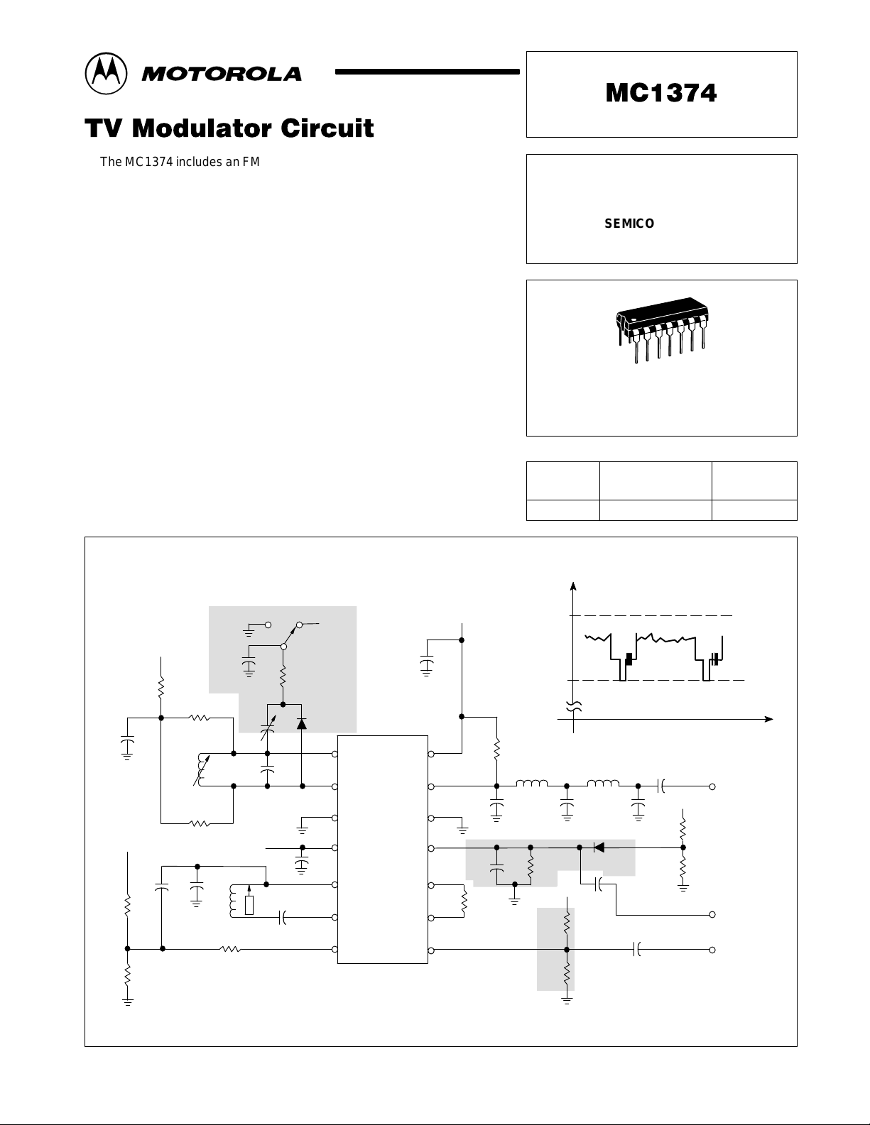
Figure 1. Simplified Application
+VCC = 12V
C9
0.001
8
R7
0.22µH
Ω
U1
MC1374
75
9
C11
10
22
11
C16
12
47
R8
13
2.2k
14
Shaded Parts Optional
L3
C12
R14
56k
R12
180k
R13
30k
47
V
4
3
D2
22
C15
0.001
R9
560
R11
220
+
C6
µ
F
1
+
0.22µH
L4
1N914
+
C10
µ
F
10
C13
V
Pin 1
V
Pin
Output
Video In
Audio In
11
t
MOTOROLA ANALOG IC DEVICE DATA
Motorola, Inc. 1996 Rev 0
1
Page 2
MC1374
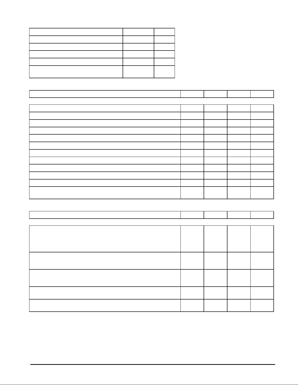
MAXIMUM RATINGS
Supply Voltage 14 Vdc
Operating Ambient Temperature Range 0 to +70 °C
Storage Temperature Range –65 to +150 °C
Junction Temperature 150 °C
Power Dissipation Package
Derate above 25°C
ELECTRICAL CHARACTERISTICS (V
AM OSCILLATOR/MODULATOR
Operating Supply Voltage 5.0 12 12 V
Supply Current (Figure 1) – 13 – mA
Video Input Dynamic Range (Sync Amplitude) 0.25 1.0 1.0 V Pk
RF Output (Pin 9, R7 = 75 Ω, No External Load) – 170 – mV pp
Carrier Suppression 36 40 – dB
Linearity (75% to 12.5% Carrier, 15 kHz to 3.58 MHz) – – 2.0 %
Differential Gain Distortion (IRE Test Signal) 5.0 7.0 10 %
Differential Phase Distortion (3.58 MHz IRE Test Signal) – 1.5 2.0 Degrees
920 kHz Beat (3.58 MHz @ 30%, 4.5 MHz @ 25%) – –57 – dB
Video Bandwidth (75 Ω Input Source) 30 – – MHz
Oscillator Frequency Range – 105 – MHz
Internal Resistance across Tank (Pin 6 to Pin 7)
Internal Capacitance across Tank (Pin 6 to Pin 7)
(TA = 25°C, unless otherwise noted.)
Rating
= 12 Vdc, TA = 25°C, fc = 67.25 MHz, Figure 4 circuit, unless otherwise noted.)
CC
Characteristics
Value Unit
1.25
10 mW/°C
W
Min Typ Max Unit
–
–
1.8
4.0
–
–
kΩ
pF
ELECTRICAL CHARACTERISTICS (T
Characteristics
FM OSCILLATOR/MODULATOR
Frequency Range of Modulator
Frequency Shift versus Temperature (Pin 14 open)
Frequency Shift versus VCC (Pin 14 open)
Output Amplitude (Pin 3 not loaded)
Output Harmonics, Unmodulated
Modulation Sensitivity 1.7 MHz
4.5 MHz
10.7 MHz
Audio Distortion (±25 kHz Deviation, Optimized Bias Pin 14)
Audio Distortion (±25 kHz Deviation, Pin 14 self biased)
Incidental AM (±25 kHz FM)
Audio Input Resistance (Pin 14 to ground)
Audio Input Capacitance (Pin 14 to ground)
Stray Tuning Capacitance (Pin 3 to ground)
Effective Oscillator Source Impedance (Pin 3 to load)
= 25°C, VCC = 12 Vdc, 4.5 MHz, Test circuit of Figure 11, unless otherwise noted.)
A
Min Typ Max Unit
14
–
–
–
–
–
–
–
–
–
–
–
–
–
–
4.5
0.2
–
900
–
0.20
0.24
0.80
0.6
1.4
2.0
6.0
5.0
5.0
2.0
14
0.3
4.0
–
–40
–
–
–
1.0
–
–
–
–
–
–
MHz
kHz/°C
kHz/V
mVpp
dB
MHz/V
%
kΩ
pF
pF
kΩ
2
MOTOROLA ANALOG IC DEVICE DATA
Page 3
MC1374
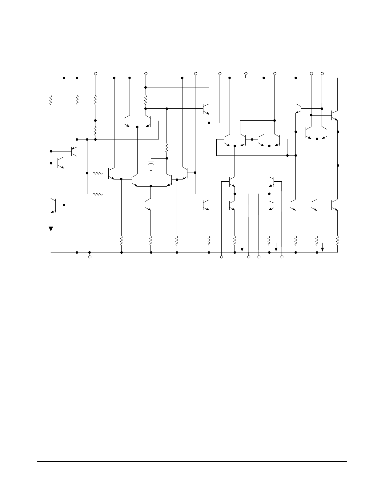
Figure 2. TV Modulator
Bias
Section
R10 R11
Q24
Q23
D1
FM Oscillator/Modulator
Audio In
14 4 3 2 8 9 7 6
R12
6.0k
R13
325
Q25
R14
Q3
R15
R1 R2 R3 R4 R5 R6 R7 R8 R9
Sound Carrier
OSC B+
R16
Q1 Q2
C1
Q4 Q5
Q26 Q27 Q8 Q9 Q16 Q17
Sound Carrier
Oscillator
Q7
Q12 Q13 Q14 Q15
R17
Q6
AM Modulator
V
CC
Q10 Q11
I = 1.15 mA1I = 1.15 mA
RF Out
1
Q21
AM Oscillator
RF Tank
Q19 Q20
2
I = 1.15 mA
Q22
Q18
5 1131211
Gnd Sound CarrierInGain Video In
GENERAL INFORMATION
The MC1374 contains an RF oscillator, RF modulator , and
a phase shift type FM modulator, arranged to permit good
printed circuit layout of a complete TV modulation system.
The RF oscillator is similar to the one used in MC1373, and is
coupled internally in the same way . Its frequency is controlled
by an external tank on Pins 6 and 7, or by a crystal circuit, and
will operate to approximately 105 MHz. The video modulator
is a balanced type as used in the well known MC1496.
Modulated sound carrier and composite video information
can be put in separately on Pins 1 and 11 to minimize
unwanted crosstalk. A single resistor on Pins 12 and 13 is
selected to set the modulator gain. The RF output at Pin 9 is
a current source which drives a load connected from Pin 9 to
V
CC.
The FM system was designed specifically for the TV
intercarrier function. For circuit economy, one phase shift
circuit was built into the ship. Still, it will operate from 1.4 MHz
to 14 MHz, low enough to be used in a cordless telephone
base station (1.76 MHz), and high enough to be used as an
FM IF test signal source (10.7 MHz). At 4.5 MHz, a deviation
of ±25 kHz can be achieved with 0.6% distortion (typical).
In the circuit above, devices Q1 through Q7 are active in
the oscillator function. Differential amplifier Q3, Q4, Q5, and
Q6 acts as a gain stage, sinking current from input section
Q1, Q2 and the phase shift network R17, C1. Input amplifier
Q1, Q2 can vary the amount of “in phase” Q4 current to be
combined with phase shifter current in load resistor R16. The
R16 voltage is applied to emitter follower Q7 which drives an
external L–C circuit. Feedback from the center of the L–C
circuit back to the base of Q6 closes the loop. As audio input
is applied which would offset the stable oscillatory phase, the
frequency changes to counteract. The input to Pin 14 can
include a dc feedback current for AFC over a limited range.
The modulated FM signal from Pin 3 is coupled to Pin 1 of
the RF modulator and is then modulated onto the AM carrier.
MOTOROLA ANALOG IC DEVICE DATA
3
Page 4

MC1374
AM Section
The AM modulator transfer function in Figure 3 shows that
the video input can be of either polarity (and can be applied at
either input). When the voltages on Pin 1 and Pin 11 are
equal, the RF output is theoretically zero. As the difference
between V
increases linearly until all of the current from both I1 current
sources (Q8 and Q9) is flowing in one side of the modulator.
This occurs when ±(V
typically 1.15 mA. The peak–to–peak RF output is the 2I1 RL.
Usually the value of RL is chosen to be 75 Ω to ease the
design of the output filter and match into TV distribution
systems. The theoretical range of input voltage and RG is
quite wide, but noise and available sound level limit the useful
video (sync tip) amplitude to between 0.25 Vpk and 1.0 Vpk.
It is recommended that the value of RG be chosen so that
only about half of the dynamic range will be used at sync tip
level.
The operating window of Figure 5 shows a cross–hatched
area where Pin 1 and Pin 1 1 voltages must always be in order
to avoid saturation in any part of the modulator. The letter φ
represents one diode drop, or about 0.75 V. The oscillator
Pins 6 and 7 must be biased to a level of V
lower) and the input Pins 1 and 1 1 must always be at least 2φ
below that. It is permissible to operate down to 1.6 V,
saturating the current sources, but whenever possible, the
minimum should be 3φ above ground.
The oscillator will operate dependably up to about
105 MHz with a broad range of tank circuit component
values. It is desirable to use a small L and a large C to
minimize the dependence on IC internal capacitance. An
operating Q between 10 and 20 is recommended. The values
of R1, R2 and R3 are chosen to produce the desired Q and to
set the Pin 6 and 7 dc voltage as discussed above.
Unbalanced operation, i.e., Pin 6 or 7 bypassed to ground, is
not recommended. Although the oscillator will still run, and
the modulator will produce a useable signal, this mode
causes substantial base–band video feedthrough.
Bandswitching, as Figure 1 shows, can still be accomplished
economically without using the unbalanced method.
The oscillator frequency with respect to temperature in the
test circuit shows less than ±20 kHz total shift from 0° to 50°C
as shown in Figure 7. At higher temperatures the slope
approaches 2.0 kHz/°C. Improvement in this region would
require a temperature compensating tuning capacitor of the
N75 family .
Crystal control is feasible using the circuit shown in Figure
21. The crystal is a 3rd overtone series type, used in series
resonance. The L1, C2 resonance is adjusted well below the
crystal frequency and is sufficiently tolerant to permit fixed
values. A frequency shift versus temperature of less than
1.0 Hz/°C can be expected from this approach. The resistors
Ra and Rb are to suppress parasitic resonances.
Coupling of output RF to wiring and components on Pins 1
and 11 can cause as much as 300 kHz shift in carrier (at
67 MHz) over the video input range. A careful layout can
keep this shift below 10 kHz. Oscillator may also be
inadvertently coupled to the RF output, with the undesired
effect of preventing a good null when V11 = V1. Reasonable
care will yield carrier rejection ratios of 36 to 40 dB below sync
tip level carrier.
Pin 11
and V
Pin11
increases, the RF output
Pin 1
– V
) = I1 RG, where I1 is
Pin1
CC – φ –2I1 RL
(or
In television, one of the most serious concerns is the
prevention of the intermodulation of color (3.58 MHz) and
sound (4.5 MHz) frequencies, which causes a 920 kHz signal
to appear in the spectrum. Very little (3rd order) nonlinearity is
needed to cause this problem. The results in Figure 6 are
unsatisfactory, and demonstrate that too much of the
available dynamic range of the MC1374 has been used.
Figures 8 and 10 show that by either reducing standard
signal level, or reducing gain, acceptable results may be
obtained.
At VHF frequencies, small imbalances within the device
introduce substantial amounts of 2nd harmonic in the RF
output. At 67 MHz, the 2nd harmonic is only 6 to 8 dB below
the maximum fundamental. For this reason, a double pi low
pass filter is shown in the test circuit of Figure 3 and works
well for Channel 3 and 4 lab work. For a fully commercial
application, a vestigial sideband filter will be required. The
general form and approximate values are shown in Figure 19.
It must be exactly aligned to the particular channel.
Figure 3. AM Modulator Transfer Function
2I1R
L
V(p–p)
RF Output
–I1R
G
Differential Input, V11–V1 (V)
0
+I1R
G
Figure 4. AM T est Circuit
R2
470
0.1
µ
H
C2 56
1
11
12 13
R
G
470
R3
76
8
9
5
0.001
R1
470
V
CC
RL
75
µ
H22
22
22 47 22
µ
H
RF
Video
Input
V
10
1.0k
V
11
L1
1
µ
F
+
4
MOTOROLA ANALOG IC DEVICE DATA
Page 5

MC1374
)
Figure 5. The Operating Window Figure 6. 920 kHz Beat
12
RL = 75
11
10
9.0
8.0
7.0
6.0
5.0
4.0
Ω
I1 = 1.15 mA
VCC – 2I1R
VCC –
φ
VCC – 3
φ
– 2I1R
3
φ
– 2I1R
V
CC
L
L
L
Recommended
V1 & V
11
Operating Region
3.0
2.0
1.0
Absolute Min = 1.6 V
φ
+ Sat)
(2
0
5.0 6.0 7.0 8.0 9.0 10 11 12
AM MODULA TOR INPUT VOLTAGE PIN 1 OR PIN 11 (V
VCC, SUPPLY VOLTAGE (Vdc)
Figure 7. RF Oscillator Frequency
versus T emperature
10
0
–10
–20
–30
–40
–50
FREQUENCY SHIFT (kHz)
–60
–70
0 25 50 75 100
TA, AMBIENT TEMPERATURE (
fc ≈ 61.25 MHz
VCC = 12 Vdc
°
C)
0
–10
[dB]
–20
–30
–40
–50
(fc) AMPLITUDE
–60
±
(fc 920 kHz) AMPLITUDE
–70
–80
0 0.1 0.2 0.3 0.4 0.5 0.6 0.7 0.8 0.9 1.0 1.1 1.2 1.3 1.4
0
–10
[dB]
–20
–30
–40
–50
(fc) AMPLITUDE
–60
±
(fc 920 kHz) AMPLITUDE
–70
–80
0 0.1 0.2 0.3 0.4 0.5 0.6 0.7 0.8 0.9 1.0 1.1 1.2 1.3 1.4
Initial Video = 1.0 Vdc
Chroma (3.58 MHz) = 300 mVpp
Sound (4.5 MHz) a) = 250 mVpp
b) = 500 mVpp
Gain Resistor RG = 1.0 k
Ω
b
a
DIFFERENTIAL INPUT (V11 – V1) [Vdc)
Figure 8. 920 kHz Beat
Initial Video = 0.5 Vdc
Chroma (3.58 MHz) = 150 mVpp
Sound (4.5 MHz) a) = 125 mVpp
Gain Resistor RG = 1.0 k
b) = 250 mVpp
Ω
b
a
DIFFERENTIAL INPUT (V11 – V1) [Vdc)
Figure 9. RF Oscillator Frequency
versus Supply V oltage
10
0
–10
–20
–30
–40
–50
NORMALIZED FREQUENCY (kHz)
–60
TA = 25°C
fc = 61.25 MHz
–70
5.0 6.0 7.0 8.0 9.0 10 11 12
VCC, SUPPLY VOLTAGE (V)
MOTOROLA ANALOG IC DEVICE DATA
0
–10
[dB]
–20
–30
–40
–50
–60
(fc) AMPLITUDE
±
(fc 920 kHz) AMPLITUDE
–70
–80
0 0.2 0.4 0.6 0.8 1.0 1.2 1.4 1.5 1.6 1.8 2.0 2.2 2.4 2.8
Figure 10. 920 kHz Beat
Initial Video = 1.0 Vdc
Chroma (3.58 MHz) = 300 mVpp
Sound (4.5 MHz) a) = 250 mVpp
Gain Resistor (RG) = 2.2 k
b) = 500 mVpp
Ω
b
a
DIFFERENTIAL INPUT (V11 – V1) [Vdc)
5
Page 6

MC1374
FM Section
The oscillator center is approximately the resonance of the
inductor L2 from Pin 2 to Pin 3 and the effective capacitance
C3 from Pin 3 to ground. For overall oscillator stability, it is
best to keep XL in the range of 300 Ω to 1.0 kΩ.
The modulator transfer characteristic at 4.5 MHz is shown
in Figure 15. Transfer curves at other frequencies have a very
similar shape, but differ in deviation per input volt, as shown in
Figures 13 and 17.
Most applications will not require DC connection to the
audio input, Pin 14. However, some improvements can be
achieved by the addition of biasing circuitry. The unaided
device will establish its own Pin 14 bias at 4 θ, or about 3.0 V .
This bias is a little too high for optimum modulation linearity.
Figure 14 shows better than 2 to 1 improvement in distortion
between the unaided device and pulling Pin 14 down to 2.6 V
to 2.7 V. This can be accomplished by a simple divider, if the
supply voltage is relatively constant.
The impedance of the divider has a bearing on the
frequency versus temperature stability of the FM system. A
divider of 180 kΩ and 30 kΩ (for VCC = 12 V) will give good
temperature stabilization results. However, as Figure 18
shows, a divider is not a good method if the supply voltage
varies. The designer must make the decisions here, based
on considerations of economy, distortion and temperature
requirements and power supply capability. If the distortion
requirements are not stringent, then no bias components are
needed. If, in this case, the temperature compensation needs
to be improved in the high ambient area, the tuning capacitor
from Pin 3 to ground can be selected from N75 or N150
temperature compensation types.
Another reason for DC input to Pin 14 is the possibility of
automatic frequency control. Where high accuracy of
inter–carrier frequency is required, it may be desirable to feed
back the DC output of an AFC or phase detector for nominal
carrier frequency control. Only limited control range could be
used without adversely affecting the distortion performance,
but very little frequency compensation will be needed.
One added convenience in the FM section is the separate
Pin “oscillator B+” which permits disabling of the sound
system during alignment of the AM section. Usually it can be
hard wired to the VCC source without decoupling.
Standard practice in television is to provide pre–emphasis
of higher audio frequencies at the transmitter and a matching
de–emphasis in the TV receiver audio amplifier. The purpose
of this is to counteract the fact that less energy is usually
present in the higher frequencies, and also that fewer
modulation sidebands are within the deviation window. Both
factors degrade signal to noise ration. Pre–emphasis of 75 µs
is standard practice. For cases where it has not been
provided, a suitable pre–emphasis network is covered in
Figure 20.
It would seem natural to take the FM system output from
Pin 2, the emitter follower output, but this output is high in
harmonic content. Taking the output from Pin 3 sacrifices
somewhat in source impedance but results in a clean output
fundamental, with all harmonics more than 40 dB down. This
choice removes the need for additional filtering components.
The source impedance of Pin 3 is approximately 2.0 kΩ, and
the open circuit amplitude is about 900 mV pp for the test
circuit shown in Figure 1 1.
The application circuit of Figure 1 shows the
recommended approach to coupling the FM output from Pin 3
to the AM modulator input, Pin 1. The input impedance at Pin
1 is very high, so the intercarrier level is determined by the
source impedance of Pin 3 driving through C4 into the video
bias circuit impedance of R4 and R5, about 2.2 k. This
provides an intercarrier level of 500 mV pp, which is correct
for the 1.0 V peak video level chosen in this design. Resistor
R6 and the input capacitance of Pin 1 provide some
decoupling of stray pickup of RF oscillator or AM output which
may be coupled to the sound circuitry .
Figure 11. FM Test Circuit
C3
f
o
(MHz)
10.7 12 10
4.5 120 10
Intercarrier
Sound Output
(Use FET Probe)
(pF)
(µ
C14
0.01
C3
120pF
L2
402001.76
H)
7
µ
F
L2
µ
H
10
C5
0.001
µ
F
6
5
4
3
2
1
Optional Bias R
(See Text)
10
12
13
14
V
CC
8
9
11
R12
C6
1
µ
F
+
Audio
Input
R13
Figure 12. Modulator Sensitivity
2.0
1.8
1.6
1.4
1.2
in
1.0
0.8
∆∆
0.6
0.4
SLOPE ( f/ V ) (MHz/V)
MAXIMUM CENTER-FREQUENCY
0.2
0
1.4 2.0 3.0 5.04.0 6.0 7.0 8.0 9.0 10 14
TA = 25°C
f
, OSCILLAT OR FREQUENCY [MHz]
osc
6
MOTOROLA ANALOG IC DEVICE DATA
Page 7

Figure 13. Modulator Transfer Function Figure 14. Distortion versus Modulation Depth
, OSCILLAT OR FREQUENCY (MHz)f
osc
f
2.1
2.0
1.9
1.8
1.7
1.6
1.5
1.4
1.3
TA = 25°C
(1.76 MHz)
0 1.0 2.0 3.0 4.0 5.0 6.0 7.0
DC INPUT VOLTAGE, PIN 14 (V)
VCC = 12 V
VCC = 5.0 V, 9.0 V
MC1374
5.0
VCC = 12 V
°
C
TA = 25
4.0
fc = 4.5 MHz
3.0
2.0
DISTORTION (%)
1.0
0
0 255075100
Self Bias (2.9–3.0 V)
Optimum Bias (2.6–2.7 V)
DEVIATION (kHz)
Figure 15. Modulator Transfer Function
4.9
4.8
4.7
4.6
4.5
4.4
4.3
, OSCILLAT OR FREQUENCY (MHz)
4.2
osc
f
4.1
TA = 25°C
(4.5 MHz)
0 1.0 2.0 3.0 4.0 5.0 6.0 7.0
DC INPUT VOLTAGE, PIN 14 (V)
VCC = 12 V
VCC = 5.0 V, 9.0 V
Figure 17. Modulator T ransfer Function Figure 18. FM System Frequency versus V
11.6
11.4
11.2
11.0
10.8
10.6
10.4
10.2
10.0
, OSCILLAT OR FREQUENCY (MHz)
9.8
osc
9.6
TA = 25°C
(10.7 MHz)
0 1.0 2.0 3.0 4.0 5.0 6.0 7.0
DC INPUT VOLTAGE, PIN 14 (V)
12 V
9.0 V V
5.0 V
CC
Figure 16. FM System Frequency
versus T emperature
4.55
4.54
VCC = 12 V
4.53
4.52
4.51
4.50
f, FREQUENCY (MHz)f, FREQUENCY (MHz)
4.49
4.48
4.47
0 2550 75100
T
, AMBIENT TEMPERATURE (
A
Pin 14 V to 2.6 V
180 k/30 k Divider
Pin 14 Open
°
C)
CC
4.50
Pin 14 to 2.6 V Source
4.49
4.48
4.47
4.46
4.45
4.44
4.43
4.42
4.0 5.0 6.0 7.0 8.0 9.0 10 11 12
Pin 14 Open
Pin14 – 180 k/ 30 k Divider
TA = 25°C
VCC, SUPPLY VOLTAGE (Vdc)
MOTOROLA ANALOG IC DEVICE DATA
7
Page 8

MC1374
V
CC
8
8.2pF
Ω
9
RL = 75
33pF
24
Ω
33pF
2.7k
8T #23 AWG
close wound on 1/8
knife tuned to trap Channel 3
61.25 MHz.
Figure 19. A Channel 4 Vestigial Sideband Filter
Both transformer windings
39
pF
4T #23 AWG
close wound on 1/4
on common axis, 3/8
8.2pF
33pF
″
ID,
24
Ω
″
ID
″
spacing.
24
100
Ω
Ω
Output
Ω
75
0
–10
–20
–30
–40
–50
–60
ATTENUATION (dB)
–70
61 65 69 73
Ch. 4
f, FREQUENCY (MHz)
Pix
Ch. 4
S
Figure 20. Audio Pre–Emphasis Circuit
1
2
π
RC
1
“Flat”
Audio
Input
CC = 0.1
–+
C = 0.0012
µ
F
r = 56k
25
20
µ
F
14
Audio
Input
Ω
6.0k
5 Gnd
R
Ω
15
10
RELATIVE OUTPUT/INPUT (dB)
–5
Pre–emphasis = 75
1
2 π (r + R)C
5
0
21 210 2100 21k
f, FREQUENCY (MHz)
µ
s = rC =
1
2
π
C
rC
2
π
(2100 Hz)
Figure 21. Crystal Controlled RF Oscillator
for Channel 3, 61.25 MHz
C1
0.001
R2
470
61.252
MC1374
NOTE: See Application Note AN829 for further information.
V
CC
R1 470
MHz
Ra
180
L1
0.15
µ
C2
56pF
H
R3
470
Rb 18
76
8
MOTOROLA ANALOG IC DEVICE DATA
Page 9

MC1374
OUTLINE DIMENSIONS
P SUFFIX
PLASTIC PACKAGE
CASE 646–06
14 8
B
17
A
F
C
N
SEATING
HG D
PLANE
K
ISSUE L
L
J
M
NOTES:
1. LEADS WITHIN 0.13 (0.005) RADIUS OF TRUE
POSITION AT SEATING PLANE AT MAXIMUM
MATERIAL CONDITION.
2. DIMENSION L TO CENTER OF LEADS WHEN
FORMED PARALLEL.
3. DIMENSION B DOES NOT INCLUDE MOLD
FLASH.
4. ROUNDED CORNERS OPTIONAL.
DIM MIN MAX MIN MAX
A 0.715 0.770 18.16 19.56
B 0.240 0.260 6.10 6.60
C 0.145 0.185 3.69 4.69
D 0.015 0.021 0.38 0.53
F 0.040 0.070 1.02 1.78
G 0.100 BSC 2.54 BSC
H 0.052 0.095 1.32 2.41
J 0.008 0.015 0.20 0.38
K 0.115 0.135 2.92 3.43
L 0.300 BSC 7.62 BSC
M 0 10 0 10
____
N 0.015 0.039 0.39 1.01
MILLIMETERSINCHES
MOTOROLA ANALOG IC DEVICE DATA
9
Page 10

MC1374
Motorola reserves the right to make changes without further notice to any products herein. Motorola makes no warranty , representation or guarantee regarding
the suitability of its products for any particular purpose, nor does Motorola assume any liability arising out of the application or use of any product or circuit, and
specifically disclaims any and all liability, including without limitation consequential or incidental damages. “T ypical” parameters which may be provided in Motorola
data sheets and/or specifications can and do vary in different applications and actual performance may vary over time. All operating parameters, including “Typicals”
must be validated for each customer application by customer’s technical experts. Motorola does not convey any license under its patent rights nor the rights of
others. Motorola products are not designed, intended, or authorized for use as components in systems intended for surgical implant into the body, or other
applications intended to support or sustain life, or for any other application in which the failure of the Motorola product could create a situation where personal injury
or death may occur. Should Buyer purchase or use Motorola products for any such unintended or unauthorized application, Buyer shall indemnify and hold Motorola
and its officers, employees, subsidiaries, affiliates, and distributors harmless against all claims, costs, damages, and expenses, and reasonable attorney fees
arising out of, directly or indirectly, any claim of personal injury or death associated with such unintended or unauthorized use, even if such claim alleges that Motorola
was negligent regarding the design or manufacture of the part. Motorola and are registered trademarks of Motorola, Inc. Motorola, Inc. is an Equal
Opportunity/Affirmative Action Employer.
How to reach us:
USA/EUROPE/Locations Not Listed: Motorola Literature Distribution; JAP AN: Nippon Motorola Ltd.; Tatsumi–SPD–JLDC, 6F Seibu–Butsuryu–Center,
P.O. Box 20912; Phoenix, Arizona 85036. 1–800–441–2447 or 602–303–5454 3–14–2 Tatsumi Koto–Ku, Tokyo 135, Japan. 03–81–3521–8315
MFAX: RMF AX0@email.sps.mot.com – TOUCHT ONE 602–244–6609 ASIA/PACIFIC: Motorola Semiconductors H.K. Ltd.; 8B Tai Ping Industrial Park,
INTERNET: http://Design–NET.com 51 Ting Kok Road, Tai Po, N.T., Hong Kong. 852–26629298
10
◊
MOTOROLA ANALOG IC DEVICE DATA
MC1374/D
*MC1374/D*
 Loading...