

Page 1
Device
Operating
Temperature Range
Package
SEMICONDUCTOR
TECHNICAL DATA
100 MHz VIDEO PROCESSOR
WITH OSD INTERFACE
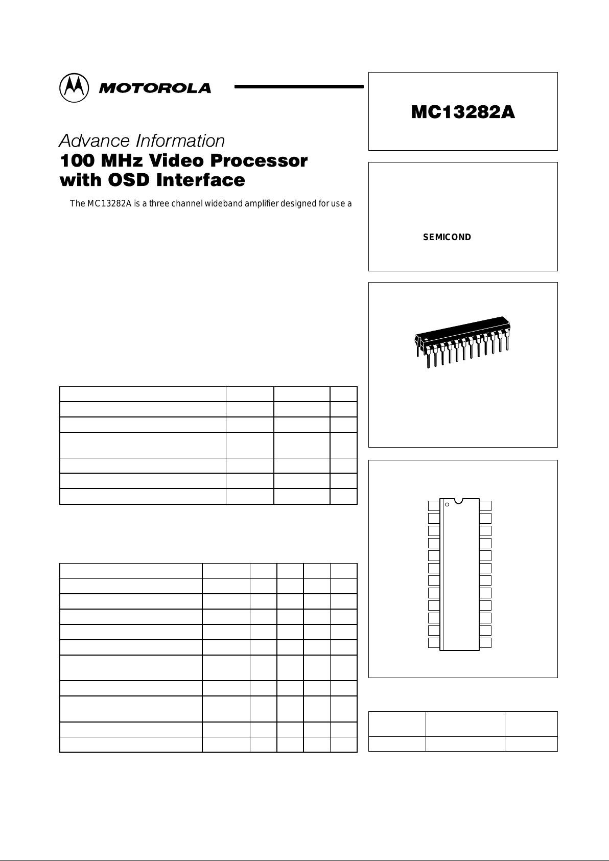
ORDERING INFORMATION
MC13282AP TA = 0° to +70°C Plastic DIP
P SUFFIX
PLASTIC PACKAGE
CASE 724
24
1
Order this document by MC13282A/D
PIN CONNECTIONS
124
23
22
21
20
19
18
17
2
3
4
5
6
7
8
(Top View)
R Subcontrast
R Input
G Subcontrast
B Input
Gnd
R
OSD
Blank
Video V
CC
16
15
14
13
9
10
11
12
G
OSD
OSD Contrast
B
OSD
Contrast
G Input
B Subcontrast
V
CC
Clamp
R Emitter
R Clamp
V5
G Emitter
G Clamp
Fast Commutate
B Clamp
B Emitter
NDIP–24
1
MOTOROLA ANALOG IC DEVICE DATA
The MC13282A is a three channel wideband amplifier designed for use as
a video pre–amp in high resolution RGB color monitors.
Features:
• 4.0 Vpp Output with 100 MHz Bandwidth
• 3.5 ns Rise/Fall Time
• Subcontrast Control for Each Channel
• Blanking and Clamping Inputs
• Contrast Control
• OSD Interface with 50 MHz Bandwidth
• OSD Contrast Control
• Package: NDIP–24
ABSOLUTE MAXIMUM RATINGS
Rating Pin Value Unit
Power Supply Voltage – V
CC
9 –0.5, 10 Vdc
Power Supply Voltage – Video V
CC
17 –0.5, 10 Vdc
Voltage at Video Amplifier Inputs 2, 4, 6, 8,
10, 12
–0.5, +5.0 Vdc
Collector–Emitter Current (Three Channels) 17 120 mA
Storage Temperature – –65 to +150 °C
Junction Temperature – 150 °C
NOTES: 1.Devices should not be operated at these limits. Refer to “Recommended
Operating Conditions” section for actual device operation.
2.ESD data available upon request.
RECOMMENDED OPERATING CONDITIONS
Characteristic Pin Min Typ Max Unit
Power Supply Voltage 9, 17 7.6 8.0 8.4 Vdc
Contrast Control 13 0 – 5.0 Vdc
Subcontrast Control 1, 3, 5 0 – 5.0 Vdc
Blanking Input Signal Amplitude 24 0 – 5.0 V
Clamping Input Signal Amplitude 23 0 – 5.0 V
Video Signal Amplitude
(with 75 Ω Termination)
2, 4, 6 – 0.7 1.0 Vpp
OSD Signal Input 8, 10, 12 – TTL – V
Collector–Emitter Current
(Total for Three Channels)
17 0 – 50 mA
Clamping Pulse Width 23 500 – – ns
Operating Ambient Temperature – 0 – 70 °C
This document contains information on a new product. Specifications and information herein
are subject to change without notice.
Motorola, Inc. 1996 Rev 0
Page 2
MC13282A
2
MOTOROLA ANALOG IC DEVICE DATA
ELECTRICAL CHARACTERISTICS
(Refer to Test Circuit Figure 1, TA = 25°C, VCC = 8.0 Vdc.)
Characteristic
Condition Pin Min Typ Max Unit
Input Impedance
– 2, 4, 6
100 – – kΩ
Internal DC Bias Voltage
– 2.4 – Vdc
Output Signal Amplitude
V2, V4, V6 = 0.7 Vpp
15, 19, 22
3.6 4.0 – Vpp
Voltage Gain
V1, V3, V5, V13
= 5.0
V
V14 = 0 V
– 5.6 – V/V
Contrast Control V13 = 5.0 to 0 V
V1, V3, V5 = 5.0 V
13 – –26 – dB
Subcontrast Control V1, V3, V5 = 5.0 to 0 V
V13 = 5.0 V
1, 3, 5 – –26 – dB
Emitter DC Level – 15, 19, 22 1.0 1.2 1.4 Vdc
Blanking Input Threshold – 24 – 1.25 – V
Clamping Input Threshold – 23 – 3.75 – V
Video Rise Time
V2, V4, V6 = 0.7 Vpp
15, 19, 22
– 3.5 –
ns
Video Fall Time
V
out
=
4.0 V
pp
RL > 300 Ω, CL < 5.0 pF
– 3.5 –
Video Bandwidth V2, V4, V6 = 0.7 Vpp
V1, V3, V5, V13 = 5.0 V
V14 = 0 V
RL > 300 Ω, CL < 5.0 pF
15, 19, 22 – 100 – MHz
OSD Rise Time
V8, V10, V12 = TTL Level
15, 19, 22
– 7.0 –
ns
OSD Fall Time
V11 = 5.0 V, V14 = 5.0 V
– 7.0 –
OSD Bandwidth V8, V10, V12 = TTL Level
V11 = 5.0 V, V14 = 5.0 V
15, 19, 22 – 50 – MHz
OSD Propagation Delay – – – 17 – ns
Power Supply Current VCC, Video VCC = 8.0 V 9, 17 – 70 – mA
NOTE: It is recommended to use a double sided PCB layout for high frequency measurement (e.g., rise/fall time, bandwidth).
Page 3
MC13282A
3
MOTOROLA ANALOG IC DEVICE DATA
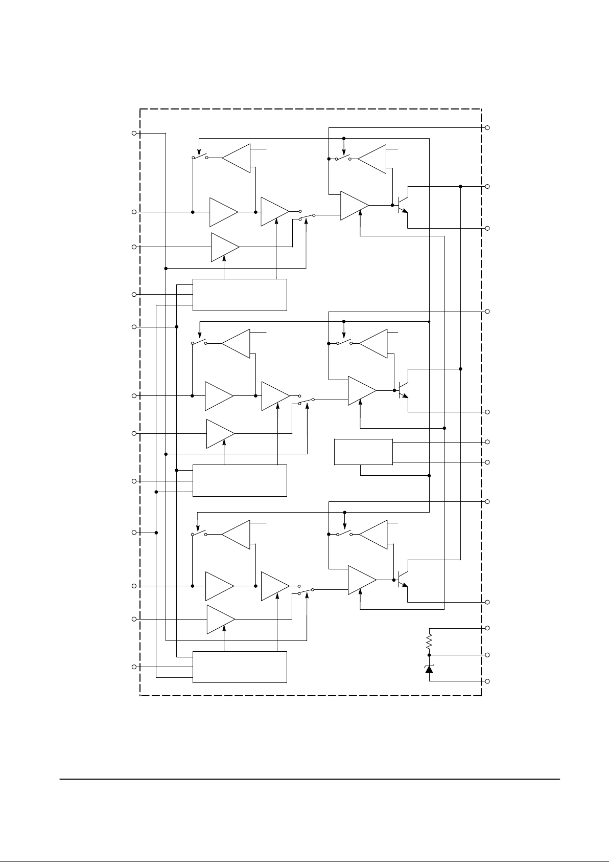
Figure 1. Internal Block Diagram
2
Fast Commutate
14
R Input
R
OSD
R Subcontrast
Contrast
G Input
G
OSD
G Subcontrast
OSD Contrast
B Input
B
OSD
B Subcontrast
R Clamp
Video V
CC
R Emitter
G Clamp
G Emitter
Blank
Clamp
B Clamp
B Emitter
V
CC
V5
Gnd
V
ref1
V
ref1
V
ref1
V
ref2
V
ref2
V
ref2
R Channel
G Channel
B Channel
Clamp Blank
Decoder
Contrast and Subcontrast
Control Processor
Contrast and Subcontrast
Control Processor
Contrast and Subcontrast
Control Processor
8
1
13
4
10
3
11
6
12
5
21
17
22
18
19
24
23
16
15
9
20
7
This device contains 272 active transistors.
Page 4
MC13282A
4
MOTOROLA ANALOG IC DEVICE DATA
PIN FUNCTION DESCRIPTION
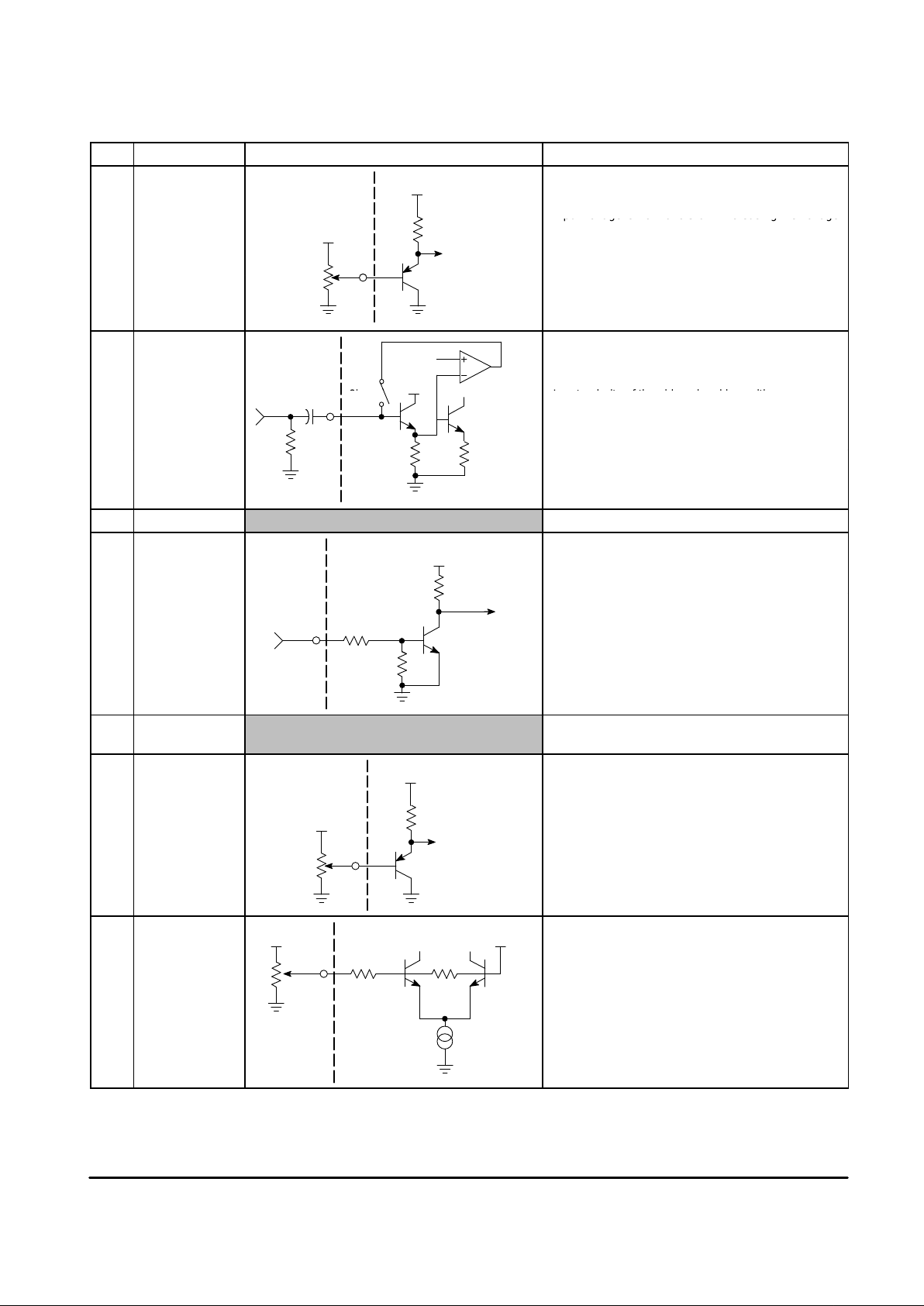
Pin Name Equivalent Internal Circuit Description
1 R Subcontrast
Control
V
CC
These pin provides a maximum of 26 dB attenuation
to vary the gain of each video amplifier separately.
Input voltage is from 0 to 5.0 V . Increasing the voltage
3 G Subcontrast
Control
5.0 V
50 k
Input voltage is from 0 to 5.0 V. Increasing the voltage
will increase the contrast level.
5 B Subcontrast
Control
2 R Input
5.0 V
V
ref
The input coupling capacitor is used for input
clamping storage. The maximum source impedance
is 100 Ω.
4 G Input
5.0 V
Clamp
75
Ω
0.1
Input polarity of the video signal is positive.
Nominal 0.7 Vpp input signal is recommended
(maximum 1.0 Vpp).
6 B Input
1.0 k10 k
75
Ω
7 Ground Ground pin. Connect to a clean, solid ground.
8 R
OSD
Input
V
CC
These inputs are standard TTL level.
10 G
OSD
Input
80 k
12 B
OSD
Input
60 k
9 V
CC
Connect to 8.0 Vdc supply, ±5%. Decoupling is
required at this pin.
11 OSD Contrast
5.0 V
V
CC
3.5 k
On Screen Display contrast control.
Input voltage is from 0 to 5.0 V . Increasing the voltage
will increase the contrast of the OSD signal.
13 Contrast
2.5 V
42 k
5.0 V
2.0 k
Overall Contrast Control for the three channels.
The input range is 0 V to 5.0 V . An increase of voltage
increases the contrast.
Page 5

MC13282A
5
MOTOROLA ANALOG IC DEVICE DATA
PIN FUNCTION DESCRIPTION (continued)
Pin Description Equivalent Internal CircuitName
14 Fast Commutate
V
CC
40 k
20 k
This pin is used in conjunction with the RGB OSD
inputs. It is a high speed switch used for overlaying
text on picture. A logic low selects Pins 2, 4, 6. A logic
high selects Pins 8, 10, 12.
15 B Emitter Output
V
CC
The video outputs are configured as emitter–followers
with a driving capability of about 15 mA each.
The dc voltage at these three emitters is set to 1.2 V
19 G Emitter Output
Video
Signal
The dc voltage at these three emitters is set to 1.2 V
(black level).
The dc current through the output stage is determined
by the emitter resistors (typically 330 Ω).
22 R Emitter Output
RE = 330
Typical
Cont
ras
t
by the emitter resistors (typically 330 Ω).
16 B Clamp
Capacitor
1.2 V
Video Out
A 100 nF capacitor is connected to each of these pins.
The capacitor is used for video output dc restoration.
18 G Clamp
Capacitor
V
CC
21 R Clamp
Capacitor
17 Video V
CC
Connect to 8.0 V dc supply, ±5%. This VCC is for the
video output stage. It is internally connected to the
collectors of the output transistors.
20 5.0 V
ref
(V5)
V
CC
Band Gap
Regulator
5.0 V
10
µ
F
0.8 RR
5.0 V regulator. Minimum 10 µF capacitor is required
for noise filtering and compensation. It can source
up to 20 mA but not sink current. Output impedance
is ≈ 10 Ω. Recommended for use as a voltage
reference only.
Page 6

MC13282A
6
MOTOROLA ANALOG IC DEVICE DATA
PIN FUNCTION DESCRIPTION (continued)
Pin Description Equivalent Internal CircuitName
23 Clamp
V
ref1
10 k
V
CC
30 k
3.75 V
V
ref2
This pin is used for video clamping.
The threshold clamping level is 3.75 V .
24 Blank
V
ref1
10 k
V
CC
30 k
1.25 V
V
ref2
This pin is used for video blanking.
The threshold blanking level is 1.25 V .
FUNCTIONAL DESCRIPTION
The MC13282A is composed of three video amplifiers,
clamping and blanking circuitry with contrast and subcontrast
controls and OSD interface. Each video amplifier is designed
to have a –3.0 dB bandwidth of 100 MHz with a gain of up to
about 5.6 V/V, or 15 dB.
Video Input
The video input stages are high impedance and designed
to accept a maximum signal of 1.0 Vpp with 75 Ω termination
(typically) provided externally. During the clamping period, a
current is provided to the input capacitor by the clamping
circuit which brings the input to a proper dc level (nominal
2.0 V). The blanking and clamping signals are to be provided
externally, with their thresholds sitting at 1.25 V and 3.75 V,
respectively.
Video Output
The video output stages are configured as
emitter–followers, with a driving capability of about 15 mA for
each channel. The dc voltage at these three emitters is set to
1.2 V (black level). The dc current through each output stage
is determined by the emitter resistor (typically 330 Ω).
Contrast Control
The contrast control varies the gain of three video
amplifiers from a minimum of 0.3 V/V to a maximum of
5.6 V/V when all subcontrast levels are set to 5.0 V.
Subcontrast Control
Each subcontrast control provides a maximum of 26 dB
attenuation on each video amplifier separately.
OSD Interface
The three OSD inputs are TTL compatible and have a
typical bandwidth of 50 MHz. A fast commutate pin is
provided to select either the video or the OSD inputs as the
source for the outputs. OSD contrast control is also
provided to set the amount of gain required when OSD
inputs are selected.
Clamp Pulse Input
The clamping pulse is provided externally, and the pulse
width must be no less than 500 ns.
Blank Pulse Input
The blanking pulse is used to blank the video signal during
the horizontal sync period, or used as a control pin for video
mute function.
Power Supplies
VCC and Video VCC supplies are to be 8.0 V ±5%.
Page 7

MC13282A
7
MOTOROLA ANALOG IC DEVICE DATA
Figure 2. Test Circuit
22
19
15
2
4
6
8
10
12
7
24 23 14 17 9
21
18
16
1311531
20
Contrast
Subcontrast Control
G
R Input
G Input
B Input
R
OSD
G
OSD
B
OSD
Gnd
V5
Blank Clamp Fast
Commutate
OSD
Contrast
Video
V
CC
V
CC
R Emitter
G Emitter
B Emitter
R Clamp
G Clamp
B Clamp
MC13282A
R175R275R3
75
Clamp
Input
OSD
Select
8.0 V
C15
0.1
R4
330R5330R6330
R Output
G Output
B Output
Clamp Capacitor
C11
0.1
C12
0.1
C13
0.1
R Input
G Input
B Input
OSD
Inputs
C1
0.1
C2
0.1
C10
0.1
C9
0.1
C8
0.1
C7
0.1
C6
0.1
C14
47
µ
F
Blank
Input
C4
0.1
C5
10
µ
F
C3
0.1
Video
Inputs
5.0 V 5.0 V 5.0 V 5.0 V 5.0 V
RB
APPLICATION INFORMATION
PCB Layout
Care should be taken in the PCB layout to minimize the
noise effects. The most sensitive pins are VCC (9), Video V
CC
(17), V5 (20), Clamp (16, 18, 21). It is strongly recommended
to make a ground plane and connect VCC/Video VCC and
ground traces to the power supply directly. Separate power
supply traces, should be used for VCC and Video VCC and
decoupling capacitors should be connected as close as
possible to the device. Multi–layer ceramic and tantalum
capacitors are recommended. Pin 20 (V5) is designed as a
5.0 V voltage reference for contrast, RGB subcontrast and
OSD contrast controls, so the same precaution for V
CC
should be also applied at this pin. The Clamp capacitors at
Pins 16,18 and 21 should be connected to ground close to
IC’s ground Pin 7 or power supply ground. The copper trace
of the video signal inputs and outputs should be as short as
possible and separated by ground traces to avoid any RGB
cross–interference. A double sided PCB should be used to
optimize the device’s performance.
RGB Input and Output
The RGB output stages are designed as emitter–followers
to drive the CRT driver circuitry directly . The emitter resistors
used is 330 Ω (typically) and the driving current is 15 mA
maximum for each channel. The loading impedance
connected to the output stages should be greater than 330 Ω
and less than 5.0 pF for optimum performance (e.g., rise/fall
time, bandwidth, etc.). Decreasing the resistive load will
reduce the rise/fall time by increasing the driving current, but
the output stage may be damaged due to increasing power
dissipation at the same time. The frequency response is
affected by the loading capacitance. The typical value is 3.0
to 5.0 pF . Figure 4 shows a typical interface with a video output
driver. For a high resolution color monitor application, it is
recommended to use coaxial cable or shielded cable for input
signal connections.
Clamp and Blank Input
The clamp input is normally (except for Sync–on–Green)
connected to a positive horizontal sync pulse, and has a
threshold level of 3.75 V. It is used as a timing reference for
the dc restoration process, so it cannot be left open. If
Sync–on–Green timing mode is used, the clamping pulse
should be located at horizontal back porch period instead of
horizontal sync tip. Otherwise, the black level will be clamped
at an incorrect voltage.
The blank input is used as a video mute, or horizontal
blanking control, and is normally connected to a blanking
Page 8

MC13282A
8
MOTOROLA ANALOG IC DEVICE DATA
pulse generated from the flyback or from an MCU. The
threshold level of 1.25 V. The blanking pulse width should be
equal to the flyback retrace period to make sure that the
video signal is blanked properly during retrace. It is
necessary to limit the amplitude, and avoid any negative
undershoots if the flyback pulse is used. This Blanking input
pin cannot accept a negative voltage. This pin should be
grounded if it is not used.
OSD interface
Figure 3 show a typical application with an OSD device
(MC141540). The MC141540 OSD and FC outputs are TTL
compatible, and therefore interface directly with MC13282A.
Level shifting circuitry is not needed. The MC141540 is a
digital device, controlled by an MCU. Therefore, separate
power supply runs to the MC141540 and to the MC13282A
are recommended. Care should be taken in the PC board
layout to prevent digital noise from entering the analog
portions of MC13282A.
Normally the OSD switching is done during the active
video time. It is recommended that the Fast Commutate pin
not be activated during the horizontal sync time.
Figure 3. Interfacing with OSD Device
C12
47
µ
F
R Input
G Input
B Input
R
OSDGOSDBOSD
Fast
Commutate
OSD
Contrast
Contrast
V
CC
V5
Clamp
R Clamp
G Clamp
B Clamp
R
Contrast
B
Contrast
G
Contrast
Blank
R Emitter
G Emitter
B Emitter
Gnd
MC13282A
Video Processor
with OSD Interface
Clamp
Input
Blank
Input
SS
MOSI
SCK
V
DD
H Tone
MC141540
On Screen Display
Processor
V
SS
V
SSA
V
DDA
H
F/B
RPVCOV
F/B
Vsyn
Input
Hsyn
Input
Video
V
CC
5.0 V
8.0 V
VR1
50 k
VR2
50 k
VR3
50 k
G Input
C1 0.1
C2 0.1
C3 0.1
R1
75
R275R3
75
5.0 V
VR5
50 k
RGB Output
C7
47
µ
FC80.1
C9
0.1
C10
0.1
C11
10
µ
F
R5
330
R6
330
R7
330
MCU Interface
V
DDA
R4
10
R8
470 k
R9
5.6 k
R10
2.0 k
R11
7.5 k
C13
0.01
C14
0.1
C15
0.1
C16
100
µ
F
C18
10
µ
F
5.0 V
L1
150 mH
C6
0.1
C5
0.1
C4
0.1
5.0 V
R
OSDGOSDBOSD
Fast
Commutate
5.0 V
VR4
50 k
C17
0.1
R Input
B Input
Page 9

MC13282A
9
MOTOROLA ANALOG IC DEVICE DATA
Figure 4. Interfacing with Video Output Drivers
C
L
CRT Driver V
CC
Reference Voltage
C12
47
µ
F
R Input
G Input
B Input
R
OSDGOSDBOSD
Fast
Commutate
OSD
Contrast
Contrast
V
CC
V5
Clamp
R Clamp
G Clamp
B Clamp
R
Contrast
B
Contrast
G
Contrast
Blank
R Emitter
G Emitter
B Emitter
Gnd
MC13282A
Video Processor
with OSD Interface
Clamp
Input
Blank
Input
Video
V
CC
5.0 V
8.0 V
VR1
50 k
VR2
50 k
VR3
50 k
G Input
C1 0.1
C2 0.1
C3 0.1
VR5
50 k
RGB Output
C9
0.1
C10
0.1
C11
10
µ
F
R5
330
R6
330
R7
330
R4
10
5.0 V
OSD Input and Control
C7
47
µ
FC80.1
R Input
B Input
C6
0.1
C5
0.1
C4
0.1
R1
75
R275R3
75
Page 10

MC13282A
10
MOTOROLA ANALOG IC DEVICE DATA
0
4.5
0
4.5
1.0
0
0
4.5
0
4.5
OSD CONTRAST CONTROL VOLTAGE (V)
CONTRAST CONTROL VOLTAGE (V)
ATTENUATION (dB)
f, FREQUENCY (MHz)
VIDEO OUTPUT (Vpp)
SUBCONTRAST VOLTAGE (V)
Figure 5. RGB In/Out Linearity
VIDEO INPUT (Vpp)
Figure 6. Color Contrast
Figure 7. Subcontrast Control Figure 8. OSD Contrast Control
Figure 9. Crosstalk From Green to Red
and Blue Channels
VIDEO OUTPUT (Vpp)
VIDEO OUTPUT (Vpp)
VIDEO OUTPUT (Vpp)
2.0
2.0
2.0
0.2
4.0
4.0
10
4.0
0.4 0.6
6.0
6.0
100
6.0
0.8
4.0
4.0
–10
4.0
4.0
3.5
3.5
–30
3.5
3.5
2.5
2.5
–50
2.5
3.0
1.5
1.5
1.5
2.0
0.5
0.5
–70
0.5
1.0
0
0
–80
0
0
2.5
1.5
0.5
3.0
2.0
1.0
3.0
2.0
1.0
3.0
2.0
1.0
–20
–40
–60
Blue Channel
Red Channel
1000
Page 11

MC13282A
11
MOTOROLA ANALOG IC DEVICE DATA
Figure 10. Rise Time Figure 11. Fall Time
100 mV/DIV
5.0 ns/DIV
10x PROBE
100 mV/DIV
5.0 ns/DIV
10x PROBE
NOTE: Recommended to use a double sided PCB without any socket for rise/fall time measurements, using an input pulse with
1.5 ns rise/fall time and an active probe with 1.7 pF capacitance loading.
Figure 12. Single Sided PCB Layout
(Component Side)
Blank Clamp
R In
G In
B In
R Out
G Out
B Out
OSD In
RGBFCInVR4
OSD
Contrast
VR5
Main
Contrast
V
CC
8.0 V
Gnd
R3
J6
C10
R4
C8
R2
R1
G VR1 G VR2 G VR3
R7
R6
C13
C4
R5
C11
C16
C12
C17
J1
C6
C1
IC2
C7
C2
C8
C3
C14
C15
J5
J2
J3
R5
J4
NOTE: J = Jumper
Page 12

MC13282A
12
MOTOROLA ANALOG IC DEVICE DATA
P SUFFIX
PLASTIC PACKAGE
CASE 724–03
ISSUE D
OUTLINE DIMENSIONS
NOTES:
1. CHAMFERED CONTOUR OPTIONAL.
2. DIMENSION L TO CENTER OF LEADS WHEN
FORMED PARALLEL.
3. DIMENSIONING AND TOLERANCING PER ANSI
Y14.5M, 1982.
4. CONTROLLING DIMENSION: INCH.
–A–
–B–
24 13
12
1
–T–
SEATING
PLANE
24 PL
K
E
F
N
C
D
G
M
A
M
0.25 (0.010) T
24 PLJ
M
B
M
0.25 (0.010) T
L
M
NOTE 1
DIM MIN MAX MIN MAX
MILLIMETERSINCHES
A 1.230 1.265 31.25 32.13
B 0.250 0.270 6.35 6.85
C 0.145 0.175 3.69 4.44
D 0.015 0.020 0.38 0.51
E 0.050 BSC 1.27 BSC
F 0.040 0.060 1.02 1.52
G 0.100 BSC 2.54 BSC
J 0.007 0.012 0.18 0.30
K 0.110 0.140 2.80 3.55
L 0.300 BSC 7.62 BSC
M 0 15 0 15
N 0.020 0.040 0.51 1.01
____
Motorola reserves the right to make changes without further notice to any products herein. Motorola makes no warranty , representation or guarantee regarding
the suitability of its products for any particular purpose, nor does Motorola assume any liability arising out of the application or use of any product or circuit, and
specifically disclaims any and all liability, including without limitation consequential or incidental damages. “T ypical” parameters which may be provided in Motorola
data sheets and/or specifications can and do vary in different applications and actual performance may vary over time. All operating parameters, including “Typicals”
must be validated for each customer application by customer’s technical experts. Motorola does not convey any license under its patent rights nor the rights of
others. Motorola products are not designed, intended, or authorized for use as components in systems intended for surgical implant into the body, or other
applications intended to support or sustain life, or for any other application in which the failure of the Motorola product could create a situation where personal injury
or death may occur. Should Buyer purchase or use Motorola products for any such unintended or unauthorized application, Buyer shall indemnify and hold Motorola
and its officers, employees, subsidiaries, affiliates, and distributors harmless against all claims, costs, damages, and expenses, and reasonable attorney fees
arising out of, directly or indirectly, any claim of personal injury or death associated with such unintended or unauthorized use, even if such claim alleges that
Motorola was negligent regarding the design or manufacture of the part. Motorola and are registered trademarks of Motorola, Inc. Motorola, Inc. is an Equal
Opportunity/Affirmative Action Employer.
How to reach us:
USA/EUROPE /Locations Not Listed: Motorola Literature Distribution; JAPAN: Nippon Motorola Ltd.; Tatsumi–SPD–JLDC, 6F Seibu–Butsuryu–Center,
P.O. Box 20912; Phoenix, Arizona 85036. 1–800–441–2447 or 602–303–5454 3–14–2 Tatsumi Koto–Ku, Tokyo 135, Japan. 03–81–3521–8315
MFAX: RMF AX0@email.sps.mot.com – TOUCHT ONE 602–244–6609 ASIA/PACIFIC: Motorola Semiconductors H.K. Ltd.; 8B Tai Ping Industrial Park,
INTERNET: http://Design–NET.com 51 Ting Ko k Road, Tai Po, N.T ., Hong Kong. 852–26629298
MC13282A/D
*MC13282A/D*
◊
 Loading...