

Page 1
Order this document by MC13175/D
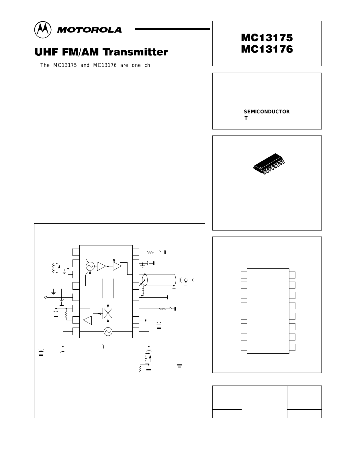
The MC13175 and MC13176 are one chip FM/AM transmitter
subsystems designed for AM/FM communication systems. They include a
Colpitts crystal reference oscillator, UHF oscillator, ÷ 8 (MC13175) or ÷ 32
(MC13176) prescaler and phase detector forming a versatile PLL system.
Targeted applications are in the 260 to 470 MHz band and 902 to 928 MHz
band covered by FCC Title 47; Part 15. Other applications include local
oscillator sources in UHF and 900 MHz receivers, UHF and 900 MHz video
transmitters, RF Local Area Networks (LANs), and high frequency clock
drivers. The MC13175/76 offer the following features:
• UHF Current Controlled Oscillator
• Uses Easily Available 3rd Overtone or Fundamental Crystals for
Reference
• Fewer External Parts Required
• Low Operating Supply Voltage (1.8 to 5.0 Vdc)
• Low Supply Drain Currents
• Power Output Adjustable (Up to +10 dBm)
• Differential Output for Loop Antenna or Balun Transformer Networks
• Power Down Feature
• ASK Modulated by Switching Output On and Off
• (MC13175) f
= 8 x f
o
; (MC13176) fo = 32 x f
ref
ref
UHF FM/AM
TRANSMITTER
SEMICONDUCTOR
TECHNICAL DATA
16
1
D SUFFIX
PLASTIC PACKAGE
CASE 751B
(SO–16)
Figure 1. T ypical Application as 320 MHz AM Transmitter
AM Modulator
Tank
Coilcraft
150–05J08
(2)
V
EE
150p
Osc
0.1
µ
0.165
1.0k
1
2
3
µ
4
f/N
5
6
7
8
100p
(MC13176)
V
CC
1. 50 Ω coaxial balun, 1/10 wavelength at 320 MHz equals 1.5 inches.
NOTES:
2. Pins 5, 10 & 15 are ground and connected to VEE which is the component/DC ground plane
2. side of PCB. These pins must be decoupled to VCC; decoupling capacitors should be placed
2. as close as possible to the pins.
3. The crystal oscillator circuit may be adjusted for frequency with the variable inductor
3. (MC13175); recommended source is Coilcraft “slot seven” 7mm tuneable inductor, Part
3. #7M3–821. 1.0k resistor. Shunting the crystal prevents it from oscillating in the fundamental
3. mode.
30p
(MC13175)
MC13175–30p
MC13176–180p
3rd Overtone
40.0000 MHz
MC13175
Crystal
16
15
14
13
12
11
10
1.0k
9
0.82
1.3k
S
2
µ
0.01
V
EE
(1)
Z = 50
RFC
1
EE
27k
µ
0.01
MC13176
(3)
Fundamental
0.1
Crystal
10 MHz
V
µ
PIN CONNECTIONS
I
1
150p
Ω
V
CC
S
1
µ
V
CC
SMA
RF
out
Osc 1
NC
NC
Osc 4
V
EE
I
Cont
PD
out
Xtale
2
3
4
5
6
7
8
16
15
14
13
12
11
10
9
mod
Out
Gnd
Out 2
Out 1
V
CC
Enable
Reg.
Gnd
Xtalb
ORDERING INFORMATION
Operating
Device
MC13175D
MC13176D
Temperature Range
TA = – 40° to +85°C
Package
SO–16
SO–16
MOTOROLA RF/IF DEVICE DATA
Motorola, Inc. 1998 Rev 1.1
1
Page 2
MC13175 MC13176
MAXIMUM RATINGS ( T
Rating Symbol Value Unit
Power Supply Voltage V
Operating Supply Voltage Range V
Junction Temperature T
Operating Ambient Temperature T
Storage Temperature
ELECTRICAL CHARACTERISTICS (Figure 2; V
Supply Current (Power down: I11 & I16 = 0) – I
Supply Current (Enable [Pin 11] to VCC thru 30 k, I16 = 0) – I
Total Supply Current (Transmit Mode)
(I
= 2.0 mA; fo = 320 MHz)
mod
Differential Output Power (fo = 320 MHz; V
= 500 mV
I
mod
I
mod
Hold–in Range (± ∆f
MC13175 (see Figure 7)
MC13176 (see Figure 8)
Phase Detector Output Error Current
MC13175
MC13176
Oscillator Enable Time (see Figure 27) 11 & 8 t
Amplitude Modulation Bandwidth (see Figure 29) 16 BW
Spurious Outputs (I
Spurious Outputs (I
Maximum Divider Input Frequency
Maximum Output Frequency
* For testing purposes, VCC is ground (see Figure 2).
; fo = N x f
p–p
= 2.0 mA (see Figures 7 and 8)
= 0 mA
mod
mod
= 25°C, unless otherwise noted.)
A
Characteristic
ref
x N)
ref
= 2.0 mA)
= 0 mA)
ref
)
CC
CC
J
A
T
stg
[Pin 9]
7.0 (max) Vdc
1.8 to 5.0 Vdc
+150 °C
– 40 to + 85 °C
– 65 to +150 °C
= – 3.0 Vdc, TA = 25°C, unless otherwise noted.)*
EE
Pin Symbol Min Typ Max Unit
– I
13 & 14 P
13 & 14 ± ∆f
7 l
13 & 14
13 & 14
–
13 & 14
EE1
EE2
EE3
out
error
enable
AM
P
son
P
soff
f
div
f
o
– 0.5 – – µA
–18 –14 – mA
–39 –34 – mA
dBm
2.0
–
H
3.5
4.0
20
22
– 4.0 – ms
– 25 – MHz
–
–
–
–
+ 4.7
–45
6.5
8.0
25
27
–50
–50
950
950
–
–
–
–
–
–
–
–
–
–
MHz
µA
dBc
MHz
Figure 2. 320 MHz Test Circuit
Osc
Tank
(1)
EE
Coilcraft
150–03J0
8
0.1
µ
27p
10p
(MC13175)
V
15p
(MC13176)
NOTES: 1. VCC is ground; while VEE is negative with respect to ground.
2.Pins 5, 10 and 15 are brought to the circuit side of the PCB via plated through holes.
They are connected together with a trace on the PCB and each Pin is decoupled to V
3.Recommended source is Coilcraft “slot seven” inductor, part number 7M3–821.
0.098
10k
1
2
3
µ
4
5
6
7
8
2.2k
2
f/N
MC13175–30p
MC13176–33p
MC13175
Crystal
3rd Overtone
40 MHz
16
15
14
13
12
11
10
9
0.82
1.0k
(ground).
CC
I
mod
10k
µ
0.1
V
CC
(1)
0.01
µ
(3)
51
51
I
reg. enable
30k
0.1
µ
µ
MC13176
Crystal
Fundamental
10 MHz
0.1
µ
0.01
0.01
RF
CC
RF
out 1
out 2
µ
µ
V
MOTOROLA RF/IF DEVICE DATA
Page 3
Pin Symbol
MC13175 MC13176
PIN FUNCTION DESCRIPTIONS
Internal Equivalent
Circuit
Description/External
Circuit Requirements
1 & 4 Osc 1,
Osc 4
5 V
6 I
EE
Cont
10k
1
0sc 1
V
EE
I
Cont
V
CC
10k
4
Osc 4
V
EE
5
6
Subcon
V
EE
V
CC
Reg
CCO Inputs
The oscillator is a current controlled type. An external oscillator
coil is connected to Pins 1 and 4 which forms a parallel
resonance LC tank circuit with the internal capacitance of the
IC and with parasitic capacitance of the PC board. Three
base–emitter capacitances in series configuration form the
capacitance for the parallel tank. These are the base–emitters
at Pins 1 and 4 and the base–emitter of the differential amplifier.
The equivalent series capacitance in the differential amplifier is
varied by the modulating current from the frequency control
circuit (see Pin 6, internal circuit). A more thorough discussion
is found in the Applications Information section.
Supply Ground (VEE)
In the PCB layout, the ground pins (also applies to Pins 10 and
15) should be connected directly to chassis ground. Decoupling
capacitors to VCC should be placed directly at
the ground returns.
Frequency Control
For VCC = 3.0 Vdc, the voltage at Pin 6 is approximately 1.55
Vdc. The oscillator is current controlled by the error current from
the phase detector. This current is amplified to drive the current
source in the oscillator section which controls the frequency of
the oscillator. Figures 9 and 10 show the ∆f
Figure 5 shows the ∆f
+85°C for 320 MHz. The CCO may be FM modulated as shown
in Figures 18 and 19, MC13176 320 MHz FM Transmitter. A
detailed discussion is found in the Applications Information
section.
osc
versus I
Cont
versus I
osc
at – 40°C, + 25°C and
Cont
,
7 PD
out
4.0k
MOTOROLA RF/IF DEVICE DATA
V
CC
4.0k
PD
out
7
Phase Detector Output
The phase detector provides ± 30 µA to keep the CCO locked at
the desired carrier frequency. The output impedance of the
phase detector is approximately 53 kΩ. Under closed loop
conditions there is a DC voltage which is dependent upon the
free running oscillator and the reference oscillator frequencies.
The circuitry between Pins 7 and 6 should be selected for
adequate loop filtering necessary to stabilize and filter the loop
response. Low pass filtering between Pin 7 and 6 is needed so
that the corner frequency is well below the sum of the divider
and the reference oscillator frequencies, but high enough to
allow for fast response to keep the loop locked. Refer to the
Applications Information section regarding loop filtering and FM
modulation.
3
Page 4
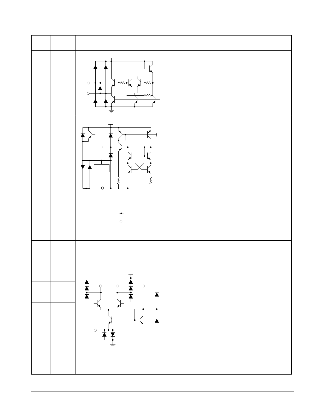
MC13175 MC13176
9
ypp
5.0p
PIN FUNCTION DESCRIPTIONS
Pin Symbol
8 Xtale
9 Xtalb
10 Reg. Gnd
11 Enable
Internal Equivalent
Circuit
V
CC
Xtalb 12k8.0k
8
Xtale
V
CC
11
Enable
Subcon
10
Reg. Gnd
8.0k
5.0p
2.4k
4.0k
Reg
Description/External
Circuit Requirements
Crystal Oscillator Inputs
The internal reference oscillator is configured as a common
emitter Colpitts. It may be operated with either a fundamental
or overtone crystal depending on the carrier frequency and the
internal prescaler. Crystal oscillator circuits and specifications
of crystals are discussed in detail in the applications section.
With VCC = 3.0 Vdc, the voltage at Pin 8 is approximately 1.8
Vdc and at Pin 9 is approximately 2.3 Vdc. 500 to 1000 mVp–p
should be present at Pin 9. The Colpitts is biased at 200 µA;
additional drive may be acquired by increasing the bias to
approximately 500 µA. Use 6.2 k from Pin 8 to ground.
Regulator Ground
An additional ground pin is provided to enhance the stability of
the system. Decoupling to the VCC (RF ground) is essential; it
should be done at the ground return for Pin 10.
Device Enable
The potential at Pin 11 is approximately 1.25 Vdc. When Pin 11
is open, the transmitter is disabled in a power down mode and
draws less than 1.0 µA ICC if the MOD at Pin 16 is also open
(i.e., it has no current driving it). To enable the transmitter a
current source of 10 µA to 90 µA is provided. Figures 3 and 4
show the relationship between ICC, VCC and I
that ICC is flat at approximately 10 mA for I
100 µA (I
mod
= 0).
reg. enable
reg. enable
. Note
= 5.0 to
12 V
13 & 14 Out 1 and
15 Out_Gnd
16 I
CC
Out 2
mod
15
Out_Gnd
13
Supply Voltage (VCC)
V
CC
12
V
CC
V
CC
1614
I
Out 2Out 1
mod
The operating supply voltage range is from 1.8 Vdc to 5.0 Vdc.
In the PCB layout, the VCC trace must be kept as wide as
possible to minimize inductive reactances along the trace; it is
best to have it completely fill around the surface mount
components and traces on the circuit side of the PCB.
Differential Output
The output is configured differentially to easily drive a loop
antenna. By using a transformer or balun, as shown in the
application schematic, the device may then drive an unbalanced
low impedance load. Figure 6 shows how much the Output
Power and Free–Running Oscillator Frequency change with
temperature at 3.0 Vdc; I
Output Ground
This additional ground pin provides direct access for the output
ground to the circuit board VEE.
AM Modulation/Power Output Level
The DC voltage at this pin is 0.8 Vdc with the current source
active. An external resistor is chosen to provide a source
current of 1.0 to 3.0 mA, depending on the desired output power
level at a given VCC. Figure 28 shows the relationship of Power
Output to Modulation Current, I
power output can be acquired with about 35 mA ICC.
For FM modulation, Pin 16 is used to set the desired output
power level as described above.
For AM modulation, the modulation signal must ride on a
positive DC bias offset which sets a static (modulation off)
modulation current. External circuitry for various schemes is
further discussed in the Applications Information section.
mod
= 2.0 mA.
. At VCC = 3.0 Vdc, 3.5 dBm
mod
4
MOTOROLA RF/IF DEVICE DATA
Page 5

MC13175 MC13176
DOCUMENT CONTAINS SCANNED IMAGES WHICH
COULD NOT BE PROCESSED FOR PDF FILES. FOR
COMPLETE DOCUMENT WITH IMAGES PLEASE
ORDER FROM MFAX OR THE LITERATURE
DISTRIBUTION CENTER
MOTOROLA RF/IF DEVICE DATA
5
Page 6
MC13175 MC13176
10
8.0
6.0
4.0
, SUPPLY CURRENT (mA)
CC
2.0
I
0
10
5.0
0
– 5.0
, OSCILLAT OR FREQUENCY (MHz)
–10
OSC
f
∆
–15
–40
Figure 3. Supply Current
versus Supply V oltage
I
reg. enable
I
mod
0
1.0 2.0 3.0 4.0 5.0
VCC, SUPPLY VOLTAGE (Vdc)
Figure 5. Change Oscillator Frequency
versus Oscillator Control Current
VCC = 3.0 Vdc
I
= 2.0 mA
mod
f = 320 MHz (I
Free–Running Oscillator
– 20 0 20 40 80
I
, OSCILLAT OR CONTROL CURRENT (
Cont
Cont
= 90 µA
= 0
= 0; TA = 25
– 40 °C
25 °C
85
60
µ
A)
Figure 4. Supply Current versus
Regulator Enable Current
100
VCC = 3.0 Vdc
I
= 0
mod
10
, SUPPLY CURRENT (mA)
CC
I
1.0
0.1
1.0 10 100 1000
I
reg. enable
, REGULAT OR ENABLE CURRENT (µA)
Figure 6. Change in Oscillator Frequency and
Output Power versus Ambient Temperature
4.0
∆
f
osc
3.0
°
C)
°
C
2.0
1.0
–1.0
– 2.0
, OSCILLAT OR FREQUENCY (MHz)
– 3.0
OSC
f
∆
– 4.0
0
–50
VCC = 3.0 Vdc
I
= 2.0 mA
mod
f = 320 MHz (I
Free–Running Oscillator
0 50 100
TA, AMBIENT TEMPERATURE (
= 0; TA = 25
Cont
°
C)
°
C)
5.5
P
O
5.0
4.5
4.0
, OUTPUT POWER (dBm)
O
3.5
P
3.0
41.0
40.8
40.6
40.4
40.2
40.0
39.8
, REFERENCE OSCILLAT OR FREQUENCY (MHz)
39.6
ref
–30
f
6
Figure 7. MC13175 Reference Oscillator
Frequency versus Phase Detector Current
Closed Loop Response:
VCC = 3.0 Vdc
I
= 2.0 mA
mod
ICC = 36 mA
PO = 5.4 dBm
– 20 –10 10 20 300
I7, PHASE DETECTOR CURRENT (
fo = 8.0 x f
V
ref
= 500 mV
ref
I
mod
ICC = 25 mA
PO = – 0.2 dBm
µ
A)
p–p
= 1.0 mA
10.3
10.2
10.1
10
9.9
, REFERENCE OSCILLAT OR FREQUENCY (MHz)
9.8
–30
ref
f
Figure 8. MC13176 Reference Oscillator
Frequency versus Phase Detector Current
Closed Loop Response:
VCC = 3.0 Vdc
fo = 32 x f
ref
V
= 500 mV
I
= 2.0 mA
mod
ICC = 35.5 mA
PO = 4.7 dBm
– 20 –10 10 20 300
I7, PHASE DETECTOR CURRENT (
ref
p–p
I
= 1.0 mA
mod
ICC = 22 mA
PO = –1.1 dBm
µ
A)
MOTOROLA RF/IF DEVICE DATA
Page 7

MC13175 MC13176
Figure 9. Change in Oscillator Frequency
versus Oscillator Control Current
20
10
–10
–20
, OSCILLAT OR FREQUENCY (MHz)
–30
OSC
f
∆
–40
–100
0
0 100 300 600200
I
, OSCILLAT OR CONTROL CURRENT (µA)
Cont
VCC = 3.0 Vdc
I
= 2.0 mA
mod
°
C
TA = 25
f
(I
osc
Cont @ 0
) 320 MHz
400 500
APPLICATIONS INFORMATION
Evaluation PC Board
The evaluation PCB, shown in Figures NO TAG and
NO TAG, is very versatile and is intended to be used across
the entire useful frequency range of this device. The center
section of the board provides an area for attaching all SMT
components to the circuit side and radial leaded components
to the component ground side of the PCB (see Figures
NO TAG and NO TAG). Additionally, the peripheral area
surrounding the RF core provides pads to add supporting
and interface circuitry as a particular application dictates.
This evaluation board will be discussed and referenced in
this section.
Current Controlled Oscillator (Pins 1 to 4)
It is critical to keep the interconnect leads from the CCO
(Pins 1 and 4) to the external inductor symmetrical and equal
in length. With a minimum inductor, the maximum free
running frequency is greater than 1.0 GHz. Since this
inductor will be small, it may be either a microstrip inductor,
an air wound inductor or a tuneable RF coil. An air wound
inductor may be tuned by spreading the windings, whereas
tuneable RF coils are tuned by adjusting the position of an
aluminum core in a threaded coilform. As the aluminum core
coupling to the windings is increased, the inductance is
decreased. The temperature coefficient using an aluminum
core is better than a ferrite core. The UniCoil inductors
made by Coilcraft may be obtained with aluminum cores
(Part No. 51–129–169).
Ground (Pins 5, 10 and 15)
Ground Returns: It is best to take the grounds to a
backside ground plane via plated through holes or eyelets at
the pins. The application PCB layout implements this
technique. Note that the grounds are located at or less than
100 mils from the devices pins.
Decoupling: Decoupling each ground pin to VCC isolates
each section of the device by reducing interaction between
sections and by localizing circulating currents.
Loop Characteristics (Pins 6 and 7)
Figure 11 is the component block diagram of the
MC1317XD PLL system where the loop characteristics are
described by the gain constants. Access to individual
components of this PLL system is limited, inasmuch as the
Figure 10. Change in Oscillator Frequency
versus Oscillator Control Current
20
10
0
–10
–20
, OSCILLAT OR FREQUENCY (MHz)
–30
OSC
f
∆
–40
–100
0 100 300 600200
I
, OSCILLAT OR CONTROL CURRENT (
Cont
VCC = 3.0 Vdc
I
= 2.0 mA
mod
°
C
TA = 25
f
(I
osc
Cont @ 0
) 450 MHz
400 500
µ
A)
loop is only pinned out at the phase detector output and the
frequency control input for the CCO. However, this allows for
characterization of the gain constants of these loop
components. The gain constants Kp, Ko and Kn are well
defined in the MC13175 and MC13176.
Phase Detector (Pin 7)
With the loop in lock, the difference frequency output of the
phase detector is DC voltage that is a function of the phase
difference. The sinusoidal type detector used in this IC has
the following transfer characteristic:
Ie = A Sin θ
e
The gain factor of the phase detector, Kp (with the loop in lock)
is specified as the ratio of DC output current, le to phase
error, θe:
Kp = Ie/θe (Amps/radians)
Kp = A Sin θe/θe
Sin θe ~ θe for θe ≤ 0.2 radians;
thus, Kp = A (Amps/radians)
Figures 7 and 8 show that the detector DC current is
approximately 30 µA where the loop loses lock
at θe=+
π/2 radians; therefore, Kp is 30 µA/radians.
Current Controlled Oscillator, CCO (Pin 6)
Figures 9 and 10 show the non–linear change in frequency
of the oscillator over an extended range of control current for
320 and 450 MHz applications. Ko ranges from
approximately 6.3x10⁵ rad/sec/µA or 100 kHz/µA (Figure 9)
to 8.8x10⁵ rad/sec/µA or 140 kHz/µA (Figure 10) over a
relatively linear response of control current (0 to 100 µA). The
oscillator gain factor depends on the operating range of the
control current (i.e., the slope is not constant). Included in the
CCO gain factor is the internal amplifier which can sink and
source at least 30 µA of input current from the phase
detector. The internal circuitry at Pin 6 limits the CCO control
current to 50 µA of source capability while its sink capability
exceeds 200 µA as shown in Figures 9 and 10. Further
information to follow shows how to use the full capabilities of
the CCO by addition of an external loop amplifier and filter
(see Figure 15). This additional circuitry yields at Ko =
0.145 MHz/µA or 9.1x10⁵ rad/sec/µA.
MOTOROLA RF/IF DEVICE DATA
7
Page 8

MC13175 MC13176
Figure 11. Block Diagram of MC1317XD PLL
Phase
Detector
Kp = 30
µ
A/rad
fn = fo/N
N = 8 : MC13175
N = 32 : MC13176
θ
Divider
Kn = 1/N
n(s)
=
θ
)
e(s
Pin 7
θ
)/N
o(s
θ
o(s)
Low Pass
Filter
K
f
Amplifier and
Current Controlled
Oscillator
Ko = 0.91Mrad/sec/
fo = nf
Pins 13,14
i
fi = f
ref
Pins 9,8
θ
i(s)
Loop Filtering
The fundamental loop characteristics, such as capture
range, loop bandwidth, lock–up time and transient response
are controlled externally by loop filtering.
The natural frequency (ωn) and damping factor (∂) are
important in the transient response to a step input of phase or
frequency . For a given ∂ and lock time, ωn can be determined
from the plot shown in Figure 12.
Figure 12. T ype 2 Second Order Response
1.9
1.8
1.7
1.6
1.5
1.4
1.3
1.2
1.1
1.0
0.9
0.8
0.7
(t), NORMALIZED OUTPUT RESPONSE
o
0.6
θ
0.5
0.4
0.3
0.2
0.1
0
0
ζ
= 0.1
0.2
0.3
0.4
0.5
0.6
0.7
0.8
1.0
1.5
2.0
1.0 2.0 3.0 4.0 5.0 6.0 7.0 8.0 9.0 10 11 12 13
ω
nt
Pin 6
Where:
µ
A
= Phase detector gain constant in
K
p
= µA/rad; Kp = 30 µA/rad
= Filter transfer function
K
f
= 1/N; N = 8 for the MC13175 and
K
n
= 1/N; N = 32 for the MC13176
K
o
= CCO gain constant in rad/sec/µA
= 9.1 x 10⁵ rad/sec/µA
K
o
For ∂ = 0.707 and lock time = 1.0 ms;
then ω
n = 5.0/t = 5.0 krad/sec.
The loop filter may take the form of a simple low pass
filter or a lag–lead filter which creates an additional pole at
origin in the loop transfer function. This additional pole
along with that of the CCO provides two pure integrators
(1/s2). In the lag–lead low pass network shown in Figure
13, the values of the low pass filtering parameters R1, R
and C determine the loop constants ωn
and
equations t1 = R1C and t2 = R2C are related in the loop filter
transfer functions F(s) = 1 + t2s/1 + ( t1 + t2)s.
Figure 13. Lag–Lead Low Pass Filter
V
in
R
1
R
2
C
V
O
The closed loop transfer function takes the form of a 2nd
order low pass filter given by,
H(s) = KvF(s)/s + KvF(s)
From control theory , if the loop filter characteristic has F(0) =
1, the DC gain of the closed loop, Kv is defined as,
Kv = KpKoK
n
and the transfer function has a natural frequency ,
ωn = (Kv/t1 + t2)
1/2
and a damping factor,
∂ = (ωn/2) (t2 + 1/Kv)
Rewriting the above equations and solving for the MC13176
with ∂ = 0.707 and ωn = 5.0 k rad/sec:
Kv = KpKoKn = (30) (0.91 106) (1/32) = 0.853 10
t1 + t2 = Kv/ωn2 = 0.853 106/(25 106) = 34.1 ms
t2 = 2∂/ωn = (2) (0.707)/(5 103) = 0.283 ms
t1 = (Kv/ωn2) – t2= (34.1 – 0.283) = 33.8 ms
∂. The
2
6
8
MOTOROLA RF/IF DEVICE DATA
Page 9

MC13175 MC13176
For C = 0.47 µ;
then, R1 = t1/C = 33.8 10–3/0.47 10–6 = 72 k
dthus, R2 = t2/C = 0.283 10–3/0.47 10–6 = 0.60 k
In the above example, the following standard value
components are used,
C = 0.47 µ; R2 = 620 and R′1 = 72 k – 53 k ~ 18 k
(R′1 is defined as R1 – 53 k, the output impedance of the
phase detector.)
Since the output of the phase detector is high impedance
(~50 k) and serves as a current source, and the input to the
frequency control, Pin 6 is low impedance (impedance of the
two diode to ground is approximately 500 Ω), it is imperative
that the second order low pass filter design above be
modified. In order to minimize loading of the R2C shunt
network, a higher impedance must be established to Pin 6. A
simple solution is achieved by adding a low pass network
between the passive second order network and the input to
Pin 6. This helps to minimize the loading effects on the
second order low pass while further suppressing the
sideband spurs of the crystal oscillator. A low pass filter with
R3 = 1.0 k and C2 = 1500 p has a corner frequency (fc) of
106 kHz; the reference sideband spurs are down greater
than – 60 dBc.
Figure 14. Modified Low Pass Loop Filter
18kPin 7
R
′
1
620
0.47
1.0k
R
3
R
2
C
V
CC
Pin 6
1500pC
3
Hold–In Range
The hold–in range, also called the lock range, tracking
range and synchronization range, is the ability of the CCO
frequency , fo to track the input reference signal, f
• N as it
ref
gradually shifted away from the free running frequency, ff.
Assuming that the CCO is capable of sufficient frequency
deviation and that the internal loop amplifier and filter are not
overdriven, the CCO will track until the phase error, θ
approaches ±π/2 radians. Figures 5 through 8 are a direct
measurement of the hold–in range (i.e. ∆f
ref
2π). Since sin θe cannot exceed ±1.0, as θe approaches ±π/2
the hold–in range is equal to the DC loop gain, Kv N.
±∆ωH = ± Kv N
where, Kv = KpKoK
n.
In the above example,
±∆ωH = ± 27.3 Mrad/sec
±∆fH = ± 4.35 MHz
Extended Hold–in Range
The hold–in range of about 3.4% could cause problems
over temperature in cases where the free–running oscillator
drifts more than 2 to 3% because of relatively high
temperature coefficients of the ferrite tuned CCO inductor.
This problem might worsen for lower frequency applications
where the external tuning coil is large compared to internal
capacitance at Pins 1 and 4. To improve hold–in range
performance, it is apparent that the gain factors involved
must be carefully considered.
Kn= is either 1/8 in the MC13175 or 1/32 in the
Kn= MC13176.
Kp= is fixed internally and cannot be altered.
Ko= Figures 9 and 10 suggest that there is capability
Ko= of greater control range with more current swing.
Ko= However, this swing must be symmetrical about
Ko= the center of the dynamic response. The
Ko= suggested zero current operating point for
Ko= ±100 µA swing of the CCO is at about + 70 µA
Ko= offset point.
Ka = External loop amplification will be necessary
Ka = since the phase detector only supplies ± 30 µA.
In the design example in Figure 15, an external resistor
(R5) of 15 k to VCC (3.0 Vdc) provides approximately 100 µA
of current boost to supplement the existing 50 µA internal
source current. R4 (1.0 k) is selected for approximately
0.1 Vdc across it with 100 µA. R1, R2 and R3 are selected to
set the potential at Pin 7 and the base of 2N4402 at
approximately 0.9 Vdc and the emitter at 1.55 Vdc when error
e
current to Pin 6 is approximately zero µA. C1 is chosen to
reduce the level of the crystal sidebands.
N = ±∆fH
30
µ
A
Phase
Detector
Output
µ
A
30
MOTOROLA RF/IF DEVICE DATA
Figure 15. External Loop Amplifier
VCC = 3.0Vdc
12
µ
A
C
1000p
1
R
1
7
R233k
R34.7k
68k
2N4402
R
1.0k
R
15k
5
4
1.6V
6
5, 10, 15
50
Oscillator
Control
Circuitry
9
Page 10

MC13175 MC13176
Figure 16 shows the improved hold–in range of the loop.
The ∆f
is moved 950 kHz with over 200 µA swing of control
ref
current for an improved hold–in range of ±15.2 MHz or
± 95.46 Mrad/sec.
Figure 16. MC13176 Reference Oscillator
Frequency versus Oscillator Control Current
10.6
10.4
10.2
10
9.8
9.6
, REFERENCE OSCILLAT OR FREQUENCY (MHz)
9.4
ref
–150
f
–100 – 50 50 1000
I6, OSCILLAT OR CONTROL CURRENT (
Closed Loop Response:
fo = 32 x f
ref
VCC = 3.0 Vdc
ICC = 38 mA
P
= 4.8 dB
out
I
= 2.0 mA
mod
V
= 500 mV
ref
p–p
µ
A)
Lock–in Range/Capture Range
If a signal is applied to the loop not equal to free running
frequency, ff, then the loop will capture or lock–in the
signal by making fs = fo (i.e. if the initial frequency
difference is not too great). The lock–in range can be
expressed as ∆ωL ~ ± 2∂ω
n
FM Modulation
Noise external to the loop (phase detector input) is
minimized by narrowing the bandwidth. This noise is minimal
in a PLL system since the reference frequency is usually
derived from a crystal oscillator. FM can be achieved by
applying a modulation current superimposed on the control
current of the CCO. The loop bandwidth must be narrow
enough to prevent the loop from responding to the
modulation frequency components, thus, allowing the CCO
to deviate in frequency. The loop bandwidth is related to the
natural frequency ωn. In the lag–lead design example where
the natural frequency, ωn = 5.0 krad/sec and a damping
factor, ∂ = 0.707, the loop bandwidth = 1.64 kHz.
Characterization data of the closed loop responses for both
the MC13175 and MC13176 at 320 MHz (Figures 7 and 8,
respectively) show satisfactory performance using only a
simple low–pass loop filter network. The loop filter response
is strongly influenced by the high output impedance of the
push–pull current output of the phase detector.
f
c
= 0.159/RC;
For R
= 1.0 k + R7 (R7 = 53 k) and C = 390 pF
f
c
= 7.55 kHz or ωc = 47 krad/sec
The application example in Figure 18 of a 320 MHz FM
transmitter demonstrates the FM capabilities of the IC. A high
value series resistor (100 k) to Pin 6 sets up the current
source to drive the modulation section of the chip. Its value is
dependent on the peak to peak level of the encoding data
and the maximum desired frequency deviation. The data
input is AC coupled with a large coupling capacitor which is
selected for the modulating frequency. The component
placements on the circuit side and ground side of the PC
board are shown in Figures NO TAG and NO TAG,
respectively. Figure 20 illustrates the input data of a 10 kHz
modulating signal at 1.6 Vp–p. Figures 21 and 22 depict the
deviation and resulting modulation spectrum showing the
carrier null at – 40 dBc. Figure 23 shows the unmodulated
carrier power output at 3.5 dBm for VCC = 3.0 Vdc.
For voice applications using a dynamic or an electret
microphone, an op amp is used to amplify the microphone’s
low level output. The microphone amplifier circuit is shown in
Figure 17. Figure 19 shows an application example for NBFM
audio or direct FSK in which the reference crystal oscillator is
modulated.
Figure 17. Microphone Amplifier
Data
Input
Voice
Input
Electret
Microphone
V
CC
3.3k
1.0k
10k
10k
3.9k
1.0
100k
120k
MC33171
V
CC
Data or
Audio
Output
Local Oscillator Application
To reduce internal loop noise, a relatively wide loop
bandwidth is needed so that the loop tracks out or cancels
the noise. This is emphasized to reduce inherent CCO and
divider noise or noise produced by mechanical shock and
environmental vibrations. In a local oscillator application the
CCO and divider noise should be reduced by proper
selection of the natural frequency of the loop. Additional low
pass filtering of the output will likely be necessary to reduce
the crystal sideband spurs to a minimal level.
10
MOTOROLA RF/IF DEVICE DATA
Page 11

130k
VCC = 3.8 to
3.3 Vdc
µ
0.47
620
33k
Coilcraft
146–04J08
9.1k
2N4402
1.0k
MC13175 MC13176
Figure 18. 320 MHz MC13176D FM Transmitter
Osc
T ank
15k
0.1
100k
0.146
µ
18k
1
2
3
µ
4
5
(2)
V
EE
6
f/32
7
8
RF Level Adjust
1.1k
16
0.047
15
14
13
5.0k
V
µ
(1)
50
Ω
CW
CC
510p
SMA
RF Output
to Antenna
RFC1 (3)
12
11
10
9
V
CC
V
27k
0.47
V
CC
CC
µ
Data Input
(1.6 Vp–p)
51p
51p
NOTES: 1. 50 Ω coaxial balun, 2 inches long.
2.Pins 5, 10 and 15 are grounds and connnected to VEE which is the component’s side ground plane.
These pins must be decoupled to VCC; decoupling capacitors should be placed as close as possible to the pins.
3.RFC1 is 180 nH Coilcraft surface mount inductor or 190 nH Coilcraft 146–05J08.
4.Recommended source is a Coilcraft “slot seven” 7.0 mm tuneable inductor, part #7M3–682.
5.The crystal is a parallel resonant, fundamental mode calibrated with 32 pF load capacitance.
Figure 19. 320 MHz NBFM Transmitter
Osc
T ank
Coilcraft
146–04J08
0.146
V
130k
4700p
6.2k
CC
9.1k 15k
1.0k
0.1
µ
2N4402
33k
External
Loop Amp
100p
NOTES: 1. 50 Ω coaxial balun, 2 inches long.
2.Pins 5, 10 and 15 are grounds and connnected to VEE which is the component’s side ground plane. These
pins must be decoupled to VCC; decoupling capacitors should be placed as close as possible to the pins.
3.RFC1 is 180 nH Coilcraft surface mount inductor.
4.RFC2 and RFC3 are high impedance crystal frequency of 10 MHz; 8.2 µH molded inductor gives XL > 1000 Ω..
5.A single varactor like the MV2105 may be used whereby RFC2 is not needed.
6.The crystal is a parallel resonant, fundamental mode calibrated with 32 pF load capacitance.
15k
1
2
3
µ
4
5
(2)
V
EE
6
f/32
7
8
180p
Crystal
Fundamental
10 MHz
16
15
14
13
12
11
10
9
Crystal
Fundamental
10MHz
(5)
1.0k
0.047
RFC
(6)
220p
6.8 (4)
RF Level Adjust
5.0k
µ
CW
(1)
UT–034
(3)
1
VCC (3.6 Vdc – Lithium Battery)
27k
0.47
µ
RFC
V
CC
10p
RFC
(5) MMBV432L
(4)
V
CC
470p
V
2
3
CC
SMA
V
CC
0.01
RF Output
to Antenna
1.0k
10
+
µ
Audio or
Data Input
µ
MOTOROLA RF/IF DEVICE DATA
11
Page 12

MC13175 MC13176
Figure 20. Input Data Waveform
Figure 21. Frequency Deviation
Figure 22. Modulation Spectrum Figure 23. Unmodulated Carrier
–10
–20
–30
–40
(dBc)
(dBc)
Reference Crystal Oscillator (Pins 8 and 9)
Selection of Proper Crystal: A crystal can operate in a
number of mechanical modes. The lowest resonant
frequency mode is its fundamental while higher order modes
are called overtones. At each mechanical resonance, a
crystal behaves like a RLC series–tuned circuit having a
large inductor and a high Q. The inductor Ls is series
resonance with a dynamic capacitor, Cs determined by the
elasticity of the crystal lattice and a series resistance Rs,
which accounts for the power dissipated in heating the
crystal. This series RLC circuit is in parallel with a static
capacitance, Cp which is created by the crystal block and by
the metal plates and leads that make contact with it.
Figure 24 is the equivalent circuit for a crystal in a single
resonant mode. It is assumed that other modes of resonance
are so far off frequency that their effects are negligible.
Series resonant frequency , fs is given by;
fs = 1/2π(LsCs)
1/2
and parallel resonant frequency , fp is given by;
fp = fs(1 + Cs/Cp)
1/2
Figure 24. Crystal Equivalent Circuit
L
3
Cp
R
3
C
3
the frequency separation at resonance is given by;
∆f = fp–fs = fs[1 – (1 + Cs/Cp)
1/2
]
Usually fp is less than 1% higher than fs, and a crystal exhibits
an extremely wide variation of the reactance with frequency
between fp and fs. A crystal oscillator circuit is very stable
with frequency. This high rate of change of impedance with
frequency stabilizes the oscillator, because any significant
change in oscillator frequency will cause a large phase shift
in the feedback loop keeping the oscillator on frequency .
12
MOTOROLA RF/IF DEVICE DATA
Page 13

MC13175 MC13176
Manufacturers specify crystal for either series or parallel
resonant operation. The frequency for the parallel mode is
calibrated with a specified shunt capacitance called a “load
capacitance.” The most common value is 30 to 32 pF. If the
load capacitance is placed in series with the crystal, the
equivalent circuit will be series resonance at the specified
parallel–resonant frequency. Frequencies up to 20 MHz use
parallel resonant crystal operating in the fundamental mode,
while above 20 MHz to about 60 MHz, a series resonant
crystal specified and calibrated for operation in the overtone
mode is used.
Application Examples
Two types of crystal oscillator circuits are used in the
applications circuits: 1) fundamental mode common emitter
Colpitts (Figures 1, 18, 19, and 25), and 2) third overtone
impedance inversion Colpitts (also Figures 1 and 25).
The fundamental mode common emitter Colpitts uses a
parallel resonant crystal calibrated with a 32 pf load
capacitance. The capacitance values are chosen to provide
excellent frequency stability and output power
of > 500 mVp–p at Pin 9. In Figures 1 and 25, the
fundamental mode reference oscillator is fixed tuned relying
on the repeatability of the crystal and passive network to
maintain the frequency, while in the circuit shown in Figures
18 and 19, the oscillator frequency can be adjusted with the
variable inductor for the precise operating frequency .
The third overtone impedance inversion Colpitts uses a
series resonance crystal with a 25 ppm tolerance. In the
application examples (Figures 1 and 25), the reference
oscillator operates with the third overtone crystal at
40.0000 MHz. Thus, the MC13175 is operated at 320 MHz
(fo/8 = crystal; 320/8 = 40.0000 MHz. The resistor across the
crystal ensures that the crystal will operate in the series
resonant mode. A tuneable inductor is used to adjust the
oscillation frequency; it forms a parallel resonant circuit with
the series and parallel combination of the external capacitors
forming the divider and feedback network and the
base–emitter capacitance of the device. If the crystal is
shorted, the reference oscillator should free–run at the
frequency dictated by the parallel resonant LC network.
The reference oscillator can be operated as high as
60 MHz with a third overtone crystal. Therefore, it is
possible to use the MC13175 up to at least 480 MHz and the
MC13176 up to 950 MHz (based on the maximum capability
of the divider network).
Enable (Pin 11)
The enabling resistor at Pin 1 1 is calculated by:
R
eg. enable
= VCC – 1.0 Vdc/I
reg. enable
From Figure 4, I
VCC= 3.0 Vdc R
27 kΩ resistor is adequate.
Layout Considerations
Supply (Pin 12): In the PCB layout, the VCC trace must be
kept as wide as possible to minimize inductive reactance
along the trace; it is best that VCC (RF ground) completely fills
around the surface mounted components and interconnect
traces on the circuit side of the board. This technique is
demonstrated in the evaluation PC board.
Battery/Selection/Lithium T ypes
The device may be operated from a 3.0 V lithium battery.
Selection of a suitable battery is important. Because one of
the major problems for long life battery powered equipment is
oxidation of the battery terminals, a battery mounted in a
clip–in socket is not advised. The battery leads or contact
post should be isolated from the air to eliminate oxide
build–up. The battery should have PC board mounting tabs
which can be soldered to the PCB. Consideration should be
given for the peak current capability of the battery. Lithium
batteries have current handling capabilities based on the
composition of the lithium compound, construction and the
battery size. A 1300 mA/hr rating can be achieved in the
cylindrical cell battery. The Rayovac CR2/3A
lithium–manganese dioxide battery is a crimp sealed, spiral
wound 3.0 Vdc, 1300 mA/hr cylindrical cell with PC board
mounting tabs. It is an excellent choice based on capacity
and size (1.358″ long by 0.665″ in diameter).
Differential Output (Pins 13, 14)
The availability of micro–coaxial cable and small baluns in
surface mount and radial–leaded components allows for
simple interface to the output ports. A loop antenna may be
directly connected with bias via RFC or 50 Ω resistors.
Antenna configuration will vary depending on the space
available and the frequency of operation.
AM Modulation (Pin 16)
Amplitude Shift Key: The MC13175 and MC13176 are
designed to accommodate Amplitude Shift Keying (ASK).
ASK modulation is a form of digital modulation corresponding
to AM. The amplitude of the carrier is switched between two
or more values in response to the PCM code. For the binary
case, the usual choice is On–Off Keying (often abbreviated
OOK). The resultant amplitude modulated waveform
consists of RF pulses called marks, representing binary 1
and spaces representing binary 0.
reg. enable
reg. enable
is chosen to be 75 µA. So, for a
= 26.6 kΩ, a standard value
MOTOROLA RF/IF DEVICE DATA
13
Page 14

Coilcraft
150–05J08
(2)
V
EE
Osc
Tank
150p
MC13175 MC13176
Figure 25. ASK 320 MHz Application Circuit
1
2
3
µ
4
f/N
5
6
7
8
0.1
0.165
µ
1.0k
16
15
14
13
12
11
10
R
mod
V
3.3k
0.01
EE
RFC
V
EE
µ
1
(1)
Z = 50
27k
0.1
V
µ
(4)
On–Off Keyed Input
TTL Level 10 kHz
SM
A
150p
CC
(5)
S
1
RF
Out
9
100p
(MC13176)
NOTES: 1. 50 Ω coaxial balun, 1/10 wavelength line (1.5″) provides the best
match to a 50 Ω load.
2.Pins 5, 10 and 15 are ground and connnected to VEE which is
the component/DC ground plane side of PCB. These pins must
be decoupled to VCC; decoupling capacitors should be placed
as close as possible to the pins.
3.The crystal oscillator circuit may be adjusted for frequency with
the variable inductor (MC13175); 1.0 k resistor shunting the
crystal prevents it from oscillating in the fundamental mode.
Recommended source is Coilcraft “slot seven” 7.0 mm tuneable
inductor, part #7M3–821.
V
CC
30p
(MC13175)
MC13175–30p
MC13176–180p
Figure 25 shows a typical application in which the output
power has been reduced for linearity and current drain. The
current draw on the device is 16 mA ICC (average) and
– 22.5 dBm (average power output) using a 10 kHz
modulating rate for the on–off keying. This equates to 20 mA
and – 2.3 dBm “On”, 13 mA and – 41 dBm “Off”. In Figure 26,
the device’s modulating waveform and encoded carrier are
0.01
µ
µ
MC13175
Crystal
3rd Overtone
0.82
1.0k
(3)
MC13176
Crystal
Fundamental
10 MHz
V
CC
40.0000 MHz
4.The On–Off keyed signal turns the output of the transmitter off and on with
TTL level pulses through R
by the resistor which sets I
5.S1 simulates an enable gate pulse from a microprocessor which will
enable the transmitter . (see Figure 4 to determine precise value of the
enabling resistor based on the potential of the gate pulse and the
desired enable.)
at Pin 16. The “On” power and ICC is set
mod
= VTTL – 0.8 / R
mod
. (see Figure 28).
mod
displayed. The crystal oscillator enable time is needed to set
the acquisition timing. It takes typically 4.0 msec to reach full
magnitude of the oscillator waveform (see Figure 27,
Oscillator Waveform, at Pin 8). A square waveform of 3.0 V
peak with a period that is greater than the oscillator enable
time is applied to the Enable (Pin 11).
14
MOTOROLA RF/IF DEVICE DATA
Page 15

MC13175 MC13176
Figure 26. ASK Input Waveform and Modulated Carrier
OOK Input Modulation
Pin 16
10 kHz TTL Waveform
On–Off Keying Encoded
Carrier Envelope
Pin 8
Oscillator Waveform
Figure 27. Oscillator Enable Time, T
enable
Figure 28. Power Output versus Modulation Current
10
5.0
0
– 5.0
–10
–15
, POWER OUTPUT (dBm)
O
P
–20
–25
0.1
I
, MODULATION CURRENT (mA)
mod
VCC = 3.0 Vdc
f = 320 MHz
MOTOROLA RF/IF DEVICE DATA
Analog AM
In analog AM applications, the output amplifier’s linearity
must be carefully considered. Figure 28 is a plot of Power
Output versus Modulation Current at 320 MHz, 3.0 Vdc. In
order to achieve a linear encoding of the modulating
sinusoidal waveform on the carrier, the modulating signal
must amplitude modulate the carrier in the linear portion of its
power output response. When using a sinewave modulating
signal, the signal rides on a positive DC offset called V
which sets a static (modulation off) modulation current, I
I
controls the power output of the IC. As the modulating
mod
mod
mod
.
signal moves around this static bias point the modulating
current varies causing power output to vary or to be AM
modulated. When the IC is operated at modulation current
levels greater than 2.0 mAdc the differential output stage
101.0
starts to saturate.
15
Page 16

MC13175 MC13176
In the design example, shown in Figure 29, the operating
point is selected as a tradeoff between average power output
and quality of the AM.
For VCC = 3.0 Vdc; lCC = 18.5 mA and I
= 0.5 mAdc and
mod
a static DC offset of 1.04 Vdc, the circuit shown in Figure 29
completes the design. Figures 30, 31 and 32 show the results
of – 6.9 dBm output power and 100% modulation by the 10
kHz and 1.0 MHz modulating sinewave signals. The
amplitude of the input signals is approximately 800 mVp–p.
Where R
= (VCC – 1.04 Vdc)/0.5 mA = 3.92 k, use a
mod
standard value resistor of 3.9 k.
Figure 30. Power Output of Unmodulated Carrier
Figure 29. Analog AM Transmitter
V
CC
3.0Vdc
Data
Input
800mVp–p
3.9k
R
mod
6.8
+
µ
5601.04Vdc
16
0.8Vdc
Figure 31. Input Signal and AM Modulated
Carrier for f
mod
= 10 kHz
Figure 32. Input Signal and AM Modulated
Carrier for f
= 1.0 MHz
mod
16
MOTOROLA RF/IF DEVICE DATA
Page 17

MC13175 MC13176
OUTLINE DIMENSIONS
D SUFFIX
PLASTIC PACKAGE
CASE 751B–05
(SO–16)
ISSUE J
–T–
–A–
16 9
–B–
18
8 PLP
0.25 (0.010) B
G
K
C
SEATING
PLANE
D
16 PL
0.25 (0.010) A
M
S
B
T
S
M
NOTES:
1. DIMENSIONING AND TOLERANCING PER ANSI
Y14.5M, 1982.
2. CONTROLLING DIMENSION: MILLIMETER.
3. DIMENSIONS A AND B DO NOT INCLUDE
MOLD PROTRUSION.
4. MAXIMUM MOLD PROTRUSION 0.15 (0.006)
M
S
R
X 45
_
F
J
PER SIDE.
5. DIMENSION D DOES NOT INCLUDE DAMBAR
PROTRUSION. ALLOWABLE DAMBAR
PROTRUSION SHALL BE 0.127 (0.005) TOTAL
IN EXCESS OF THE D DIMENSION AT
MAXIMUM MATERIAL CONDITION.
DIM MIN MAX MIN MAX
A 9.80 10.00 0.386 0.393
B 3.80 4.00 0.150 0.157
C 1.35 1.75 0.054 0.068
D 0.35 0.49 0.014 0.019
F 0.40 1.25 0.016 0.049
G 1.27 BSC 0.050 BSC
J 0.19 0.25 0.008 0.009
K 0.10 0.25 0.004 0.009
M 0 7 0 7
____
P 5.80 6.20 0.229 0.244
R 0.25 0.50 0.010 0.019
INCHESMILLIMETERS
Motorola reserves the right to make changes without further notice to any products herein. Motorola makes no warranty , representation or guarantee regarding
the suitability of its products for any particular purpose, nor does Motorola assume any liability arising out of the application or use of any product or circuit, and
specifically disclaims any and all liability, including without limitation consequential or incidental damages. “T ypical” parameters which may be provided in Motorola
data sheets and/or specifications can and do vary in different applications and actual performance may vary over time. All operating parameters, including “Typicals”
must be validated for each customer application by customer’s technical experts. Motorola does not convey any license under its patent rights nor the rights of
others. Motorola products are not designed, intended, or authorized for use as components in systems intended for surgical implant into the body, or other
applications intended to support or sustain life, or for any other application in which the failure of the Motorola product could create a situation where personal injury
or death may occur. Should Buyer purchase or use Motorola products for any such unintended or unauthorized application, Buyer shall indemnify and hold Motorola
and its officers, employees, subsidiaries, affiliates, and distributors harmless against all claims, costs, damages, and expenses, and reasonable attorney fees
arising out of, directly or indirectly, any claim of personal injury or death associated with such unintended or unauthorized use, even if such claim alleges that
Motorola was negligent regarding the design or manufacture of the part. Motorola and are registered trademarks of Motorola, Inc. Motorola, Inc. is an Equal
Opportunity/Affirmative Action Employer.
How to reach us:
USA/EUROPE/ Locations Not Listed: Motorola Literature Distribution; JAPAN: Nippon Motorola Ltd.: SPD, Strategic Planning Office, 141,
P.O. Box 5405, Denver, Colorado 80217. 1–303–675–2140 or 1–800–441–2447 4–32–1 Nishi–Gotanda, Shagawa–ku, Tokyo, Japan. 03–5487–8488
Customer Focus Center: 1–800–521–6274
Mfax: RMFAX0@email.sps.mot.com – TOUCHTONE 1–602–244–6609 ASIA/PACIFIC: Motorola Semiconductors H.K. Ltd.; 8B Tai Ping Industrial Park,
Moto rola Fax Back Sys tem – US & Canada ONLY 1–800–774–1848 51 Ting Kok Road, Tai Po, N.T., Hong Kong. 852–26629298
HOME PAGE: http://motorola.com/sps/
MOTOROLA RF/IF DEVICE DATA
– http://sps.motorola.com/mfax/
◊
Mfax is a trademark of Motorola, Inc.
MC13175/D
17
 Loading...