

Page 1
Order this document by MC13158/D
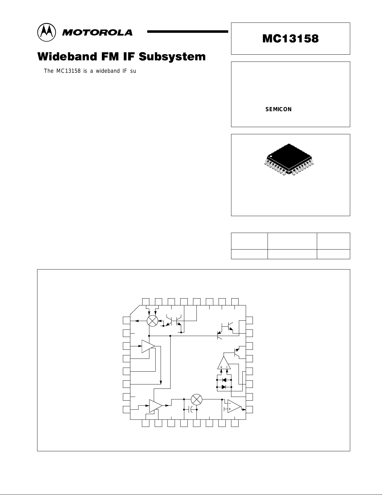
The MC13158 is a wideband IF subsystem that is designed for high
performance data and analog applications. Excellent high frequency
performance is achieved, with low cost, through the use of Motorola’s
MOSAIC 1.5 RF bipolar process. The MC13158 has an on–board
grounded collector VCO transistor that may be used with a fundamental or
overtone crystal in single channel operation or with a PLL in multi–channel
operation. The mixer is useful to 500 MHz and may be used in a balanced
differential or single ended configuration. The IF amplifier is split to
accommodate two low cost cascaded filters. RSSI output is derived by
summing the output of both IF sections. A precision data shaper has an Off
function to shut the output off to save current. An enable control is provided
to power down the IC for power management in battery operated
applications.
Applications include DECT , wideband wireless data links for personal and
portable laptop computers and other battery operated radio systems which
utilize GFSK, FSK or FM modulation.
• Designed for DECT Applications
• 1.8 to 6.0 Vdc Operating Voltage
• Low Power Consumption in Active and Standby Mode
• Greater than 600 kHz Detector Bandwidth
• Data Slicer with Special Off Function
• Enable Function for Power Down of Battery Operated Systems
• RSSI Dynamic Range of 80 dB Minimum
• Low External Component Count
WIDEBAND FM IF
SUBSYSTEM FOR DECT
AND DIGITAL APPLICATIONS
SEMICONDUCTOR
TECHNICAL DATA
32
1
FTB SUFFIX
PLASTIC PACKAGE
CASE 873
(Thin QFP)
ORDERING INFORMATION
Operating
Device
MC13158FTB TA = – 40 to +85°C TQFP–32
Temperature Range
Package
Mix Out
V
CC1
IF In
IF Dec1
IF Dec2
IF Out
V
CC2
Lim In
Representative Block Diagram
Osc
N/C
11
N/C
Osc
Emit
MC13158
Data
Slicer
5.0 p
12
Lim
Out
Base
13
Quad
Mix
Mix
In1
In2
1
2
3
4
5
6
7
8
IF Amp
LIM
Amp
10
9
Lim
Lim
Dec2
Dec1
This device contains 234 active transistors.
N/C
14
N/C
EE1
15
Det
Gain
EnableV
Bias
V
2532 31 30 29 28 27 26
16
EE2
24
23
22
21
20
19
18
17
RSSI
RSSI Buf
DS Gnd
DS Out
DS In2
DS “off”
DS In1
Det Out
MOTOROLA ANALOG IC DEVICE DATA
Motorola, Inc. 1996 Rev 1
1
Page 2

MC13158
MAXIMUM RATINGS
Rating Pin Symbol Value Unit
Power Supply Voltage 16, 26 V
Junction Temperature T
Storage Temperature Range T
NOTE: 1.Devices should not be operated at or outside these values. The “Recommended Operating
Conditions” provide for actual device operation.
S(max)
JMAX
stg
6.5 Vdc
+150 °C
–65 to +150 °C
RECOMMENDED OPERATING CONDITIONS (V
Rating
Power Supply Voltage 2, 7 V
TA = 25°C
–40°C ≤ TA≤ 85°C 16, 26
Input Frequency 31, 32 F
Ambient Temperature Range T
Input Signal Level 31, 32 V
DC ELECTRICAL CHARACTERISTICS (T
Characteristic
Total Drain Current VS = 2.0 Vdc 16, 26 I
DATA SLICER (Input Voltage Referenced to VEE; VS = 3.0 Vdc; No Input Signal)
Output Current; V18 LO; V19 = V
Data Slicer Enabled (DS “on”) V18 < V
Output Current; V18 HI; V19 = V
Data Slicer Enabled (DS “on”) V18 > V
Output Current; V19 = V
Data Slicer Disabled (DS “off”) V20 = VS/2
= 25°C; VS = 3.0 Vdc; No Input Signal; See Figure 1.)
A
Condition Pin Symbol Min Typ Max Unit
VS = 3.0 Vdc 3.5 5.7 8.5
VS = 6.0 Vdc 3.5 6.0 9.5
See Figure 2
V20 = VS/2
See Figure 3
V20 = VS/2
See Figure 4
= V2 = V7; VEE = V16 = V22 = V26; VS = VCC – VEE)
CC
Pin Symbol Value Unit
TOTAL
EE
20
EE
20
CC
21 I
21 I
21 I
21
21
21
S
in
A
in
2.5 5.5 8.5 mA
2.0 5.9 – mA
– 0.1 1.0 µA
– 0.1 1.0 µA
2.0 to 6.0 Vdc
10 to 500 MHz
–40 to +85 °C
200 mVrms
AC ELECTRICAL CHARACTERISTICS (T
Characteristic
MIXER
Mixer Conversion Gain Vin = 1.0 mVrms 31, 32, 1 – – 22 – dB
Noise Figure Input Matched 31, 32, 1 NF – 14 – dB
Mixer Input Impedance Single–Ended 31, 32 Rp – 865 – Ω
Mixer Output Impedance 1 – – 330 – Ω
2
= 25°C; VS = 3.0 Vdc; fRF = 110.7 MHz; fLO = 100 MHz; See Figure 1.)
A
Condition Pin Symbol Min Typ Max Unit
See Figure 5
See Figure 15 Cp – 1.6 – pF
MOTOROLA ANALOG IC DEVICE DATA
Page 3
MC13158
AC ELECTRICAL CHARACTERISTICS (continued) (T
Characteristic
IF AMPLIFIER SECTION
IF RSSI Slope See Figure 8 23 – 0.15 0.3 0.4 µA/dB
IF Gain f = 10.7 MHz 3, 6 – – 36 – dB
Input Impedance 3 – – 330 – Ω
Output Impedance 6 – – 330 – Ω
LIMITING AMPLIFIER SECTION
Limiter RSSI Slope See Figure 9 23 – 0.15 0.3 0.4 µA/dB
Limiter Gain f = 10.7 MHz 8, 12 – – 70 – dB
Input Impedance 8 – – 330 – Ω
Condition Pin Symbol Min Typ Max Unit
See Figure 7
= 25°C; VS = 3.0 Vdc; fRF = 110.7 MHz; fLO = 100 MHz; See Figure 1.)
A
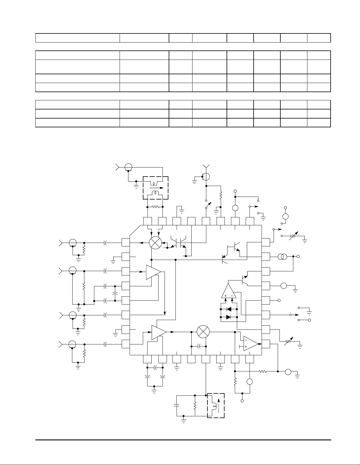
Figure 1. T est Circuit
Osc
Emit
MC13158
Lim
Out
12
LO Input
5.0 p
Base
13
100 MHz
200 mVrms
N/COsc
Data
Slicer
N/CQuad
14
100 k
1.0
µ
H
–3.0 Vdc
50
A
Det
Gain
15
V
EE1
Bias
2532 31 30 29 28 27 26
Enable
RSSI
RSSI
Buf
DS
Gnd
DS
Out
DS
In2
DS
“off”
DS
In1
Det
Out
V
EE2
16
A
51 k
24
23
22
21
20
19
18
17
–2.3 Vdc
A
0 to –3.0 Vdc
100
µ
A
A
–1.5 Vdc
0 to –3.0 Vdc
V
–3.0 Vdc
–3.0 Vdc
Mixer
Output
IF
Input
IF
Output
Limiter
Input
110.7 MHz
330
50
330
50
RF Input
1.0 n
100 n
1.0 n
100 n
1.0 n
100 n
100 n
1
2
3
4
5
6
7
8
1:4
Mix
Out
V
CC1
IF
In
IF
Dec1
IF
Dec2
IF
Out
V
CC2
Lim
In
Mix
In2
Lim
Dec1
9
200
Lim
Dec2
100 n
In1
Lim Amp
N/C
10
1.0 n1.0 n
N/CMix
11
MOTOROLA ANALOG IC DEVICE DATA
200 pF
6.8 k
–3.0 Vdc
3
Page 4
MC13158
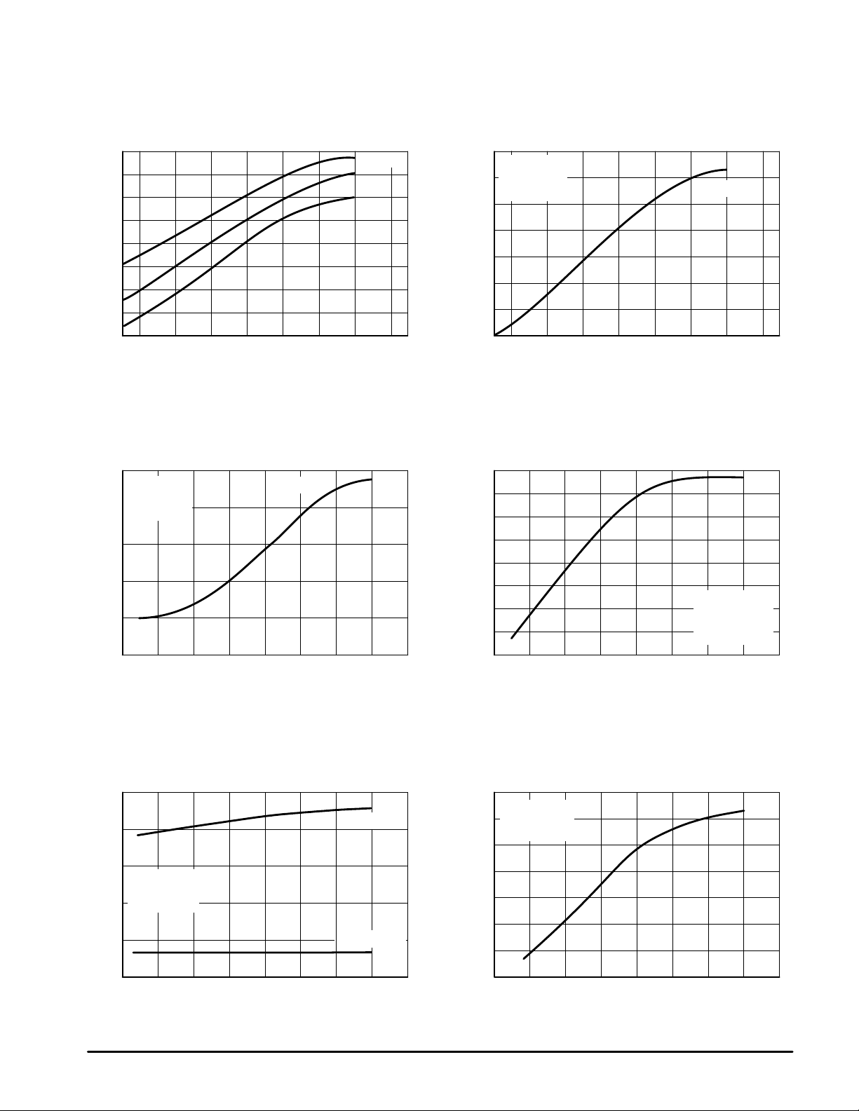
T ypical Performance Over Temperature
(per Figure 1)
6.4
6.2
6.0
5.8
5.6
5.4
5.2
, TOTAL SUPPLY CURRENT (mA)
5.0
TOTAL
I
4.8
0.12
Data Slicer “On”
µ
V19 = V
0.10
V20 = VS/2
0.08
0.06
0.04
DATA SLICER OUTPUT CURRENT ( A)
0.02
–40
Figure 2. T otal Supply Current versus
Ambient T emperature, Supply Voltage
VS = 6.0 V
3.0 V
2.0 V
DATA SLICER OUTPUT CURRENT (mA)
–20
0 20 40 60 80 100 120 0 20 40 60 80 100 120
TA, AMBIENT TEMPERATURE (°C)
Figure 4. Data Slicer On Output Current
versus Ambient T emperature
V18 > V
20
CC
– 0.1
– 0.2
– 0.3
– 0.4
NORMALIZED MIXER GAIN (dB)
– 0.5
– 20 0 20 40 60 80 100 120 – 20 0 20 40 60 80 100 120
TA, AMBIENT TEMPERATURE (°C)
– 0.6
Figure 3. Data Slicer On Output Current
versus Ambient T emperature
8.5
Data Slicer “On”
V19 = V
8.0
7.5
7.0
6.5
6.0
5.5
5.0
EE
V20 = VS/2
–20
TA, AMBIENT TEMPERATURE (°C)
Figure 5. Normalized Mixer Gain
versus Ambient T emperature
0.2
0.1
0
–40
TA, AMBIENT TEMPERATURE (°C)
V18 < V
20
Vin = 1.0 mVrms
VS = 3.0 Vdc
fc = 110.7 MHz
fLO = 100 MHz
Figure 6. Mixer RSSI Output Current versus
Ambient T emperature, Mixer Input Level
7.0
µ
6.0
5.0
VS = 3.0 Vdc
fc = 110.7 MHz
fLO = 100 MHz
4.0
3.0
MIXER RSSI OUTPUT CURRENT ( A)
2.0
– 20 0 20 40 60 80 – 20 0 20 40 60 80 100 120100 120
–40
TA, AMBIENT TEMPERATURE (°C)
4
Vin = 10 mVrms
Vin = 1.0 mVrms
0.6
VS = 3.0 Vdc
0.4
f = 10.7 MHz
Vin = 1.0 mVrms
0.2
0
– 0.2
– 0.4
NORMALIZED IF AMP GAIN (dB)
– 0.6
– 0.8
–40
Figure 7. Normalized IF Amp Gain
versus Ambient T emperature
TA, AMBIENT TEMPERATURE (°C)
MOTOROLA ANALOG IC DEVICE DATA
Page 5

MC13158
tT ypical Performance Over Temperature
(per Figure 1)
Figure 8. IF Amp RSSI Output Current versus
Ambient T emperature, IF Input Level
10
µ
9.0
8.0
7.0
VS = 3.0 Vdc
6.0
f = 10.7 MHz
5.0
4.0
3.0
IF AMP RSSI OUTPUT CURRENT ( A)
2.0
– 20 0 20 40 60 80 – 20 0 20 40 60 80 100 120100 120
–40
TA, AMBIENT TEMPERATURE (°C)
Figure 10. Total RSSI Output Current versus
Ambient T emperature (No Signal)
0.60
VS = 3.0 Vdc
µ
No Input Signal
0.55
0.50
0.45
Vin = 10 mVrms
Vin = 1.0 mVrms
Figure 9. Limiter Amp RSSI Output Current
versus Ambient T emperature, Input Signal Level
8.0
µ
Vin = 100 mVrms
6.0
LIMITER AMP RSSI OUTPUT CURRENT ( A)
4.0
2.0
– 2.0
VS = 3.0 Vdc
f = 10.7 MHz
0
–40
TA, AMBIENT TEMPERATURE (°C)
Vin = 10 mVrms
Vin = 1.0 mVrms
Vin = 100
Figure 11. Demodulator DC Voltage versus
Ambient Temperature
1.20
1.15
1.10
1.05
1.00
µ
Vrms
VS = 3.0 Vdc
R17 = 51 k
R15 = 100 k
0.40
TOTAL RSSI OUTPUT CURRENT ( A)
0.35
SYSTEM LEVEL AC ELECTRICAL CHARACTERISTICS (T
12 dB SINAD Sensitivity: fRF = 112 MHz 1 – dBm
Narrowband Application f
Without Preamp Figure 25 –101
With Preamp Figure 26 –113
Third Order Intercept Point f
1.0 dB Comp. Point VS = 3.5 Vdc 1.0 dB C.Pt. –39
NOTES: 1. Test Circuit & Test Set per Figure 24.
– 20 0 20 40 60 80 100 120
–40
TA, AMBIENT TEMPERATURE (°C)
Characteristic
f
f
RF2
2.Test Circuit & Test Set per Figure 27.
A
Condition Notes Symbol Typ Unit
= 1.0 kHz
mod
= ±125 kHz
dev
SINAD Curve
= 112 MHz 2 IIP3 –32 dBm
RF1
= 112.1 MHz
Figure 28
0.95
DEMODULATOR OUTPUT DC VOLTAGE (Vdc)
0.90
–40
– 20 0 20 40 60 80 100 120
TA, AMBIENT TEMPERATURE (°C)
= 25°C; VS = 3.0 Vdc; fRF = 112 MHz; fLO = 122.7 MHz)
MOTOROLA ANALOG IC DEVICE DATA
5
Page 6

MC13158
CIRCUIT DESCRIPTION
General
The MC13158 is a low power single conversion wideband
FM receiver incorporating a split IF . This device is designated
for use as the backend in digital FM systems such as Digital
European Cordless Telephone (DECT) and wideband data
links with data rates up to 2.0 Mbps. It contains a mixer,
oscillator, Received Signal Strength Indicator (RSSI), IF
amplifier, limiting IF, quadrature detector, power down or
enable function, and a data slicer with output off function.
Further details are covered in the Pin Function Description
which shows the equivalent internal circuit and external
circuit requirements.
Current Regulation/Enable
Temperature compensating voltage independent current
regulators which are controlled by the enable pin (Pin 25)
where “low” powers up and “high” powers down the entire
circuit.
Mixer
The mixer is a double–balanced four quadrant multiplier
and is designed to work up to 500 MHz. It can be used in
differential or in single ended mode by connecting the other
input to the positive supply rail. The linear gain of the mixer is
approximately 22 dB at 100 mVrms LO drive level. The mixer
gain and noise figure have been emphasized at the expense
of intermodulation performance. RSSI measurements are
added in the mixer to extend the range to higher signal levels.
The single–ended parallel equivalent input impedance of the
mixer is Rp ~ 1.0 kΩ and Cp ~ 2.0 pF. The buffered output of
the mixer is internally loaded resulting in an output
impedance of 330 Ω.
Local Oscillator
The on–chip transistor operates with crystal and LC
resonant elements up to 220 MHz. Series resonant, overtone
crystals are used to achieve excellent local oscillator stability .
Third overtone crystals are used through about 65 to 70 MHz.
Operation from 70 MHz up to 180 MHz is feasible using the
on–chip transistor with a 5th or 7th overtone crystal. To
enhance operation using an overtone crystal, the internal
transistor bias is increased by adding an external resistor
from Pin 29 to VEE; however, with an external resistor the
oscillator stays on during power down. Typically, –10 dBm of
local oscillator drive is needed to adequately drive the mixer.
With an external oscillator source, the IC can be operated up
to 500 MHz.
RSSI
The received signal strength indicator (RSSI) output is a
current proportional to the log of the received signal
amplitude. The RSSI current output is derived by summing
the currents from the mixer, IF and limiting amplifier stages.
An increase in RSSI dynamic range, particularly at higher
input signal levels is achieved. The RSSI circuit is designed
to provide typically 85 dB of dynamic range with temperature
compensation.
Linearity of the RSSI is optimized by using external
ceramic bandpass filters which have an insertion loss of
4.0 dB and 330 Ω source and load impedance. For higher
data rates used in DECT and related applications, LC
bandpass filtering is necessary to acquire the desired
bandpass response; however, the RSSI linearity will require
the same insertion loss.
RSSI Buffer
The RSSI output current creates a voltage across an
external resistor. A unity voltage–gain amplifier is used to
buffer this voltage. The output of this buffer has an active
pull–up but no pull–down, so it can also be used as a peak
detector. The negative slew rate is determined by external
capacitance and resistance to the negative supply .
IF Amplifier
The first IF amplifier section is composed of three
differential stages with the second and third stages
contributing to the RSSI. This section has internal DC
feedback and external input decoupling for improved
symmetry and stability. The total gain of the IF amplifier block
is approximately 40 dB at 10.7 MHz.
The fixed internal input impedance is 330 Ω. When using
ceramic filters requiring source and loss impedances of
330 Ω, no external matching is necessary. Overall RSSI
linearity is dependent on having total midband attenuation of
10 dB (4.0 dB insertion loss plus 6.0 dB impedance matching
loss) for the filter. The output of the IF amplifier is buffered
and the impedance is 330 Ω.
Limiter
The limiter section is similar to the IF amplifier section
except that five differential stages are used. The fixed internal
input impedance is 330 Ω. The total gain of the limiting
amplifier section is approximately 70 dB. This IF limiting
amplifier section internally drives the quadrature detector
section and it is also brought out on Pin 12.
Quadrature Detector
The quadrature detector is a doubly balanced four
quadrant multiplier with an internal 5.0 pF quadrature
capacitor between Pins 12 and 13. An external capacitor may
be added between these pins to increase the IF signal to the
external parallel RLC resonant circuit that provides the
90 degree phase shift and drives the quadrature detector. A
single pin (Pin 13) provides for the external LC parallel
resonant network and the internal connection to the
quadrature detector.
Internal low pass filter capacitors have been selected to
control the bandwidth of the detector. The recovered signal is
brought out by the inverting amplifier buffer. An external
feedback resistor from the output (Pin 17) to the input of the
inverting amplifier (Pin 15) controls the output amplitude; it is
combined with another external resistor from the input to the
negative supply (Pin 16) to set the output dc level. For a
resistor ratio of 1, the DC level at the detector output is
2.0 VBE (see Figure 12). A small capacitor C17 across the
first resistor (from Pin 17 to 15) can be used to reduce the
bandwidth.
Data Slicer
The data slicer is a comparator that is designed to square
up the data signal. Across the data slicer inputs (Pins 18
and 20) are back to back diodes.
6
MOTOROLA ANALOG IC DEVICE DATA
Page 7

MC13158
Á
Á
Á
Á
Á
Á
Á
Á
Á
Á
Á
Á
Á
Á
Á
Á
Á
Á
Á
Á
Á
Á
Out
Á
Á
Á
Á
Á
Oscillator, and IF Amplifer. The operating
Á
Á
Á
Á
Á
Á
Á
Á
Á
Á
Á
Á
Á
Á
Á
Á
Á
Á
Á
Á
Á
Á
Á
Á
Á
Á
Á
Á
Á
Á
Á
Á
Á
Á
Á
Á
Á
Á
Á
Á
Á
Á
Á
Á
Á
Á
Á
Á
The recovered data signal from the quadrature detector
can be DC coupled to the data slicer DS IN1 (Pin 18). In the
application circuit shown in Figure 1 it will be centered at
2.0 VBE and allowed to swing ± VBE. A capacitor is placed
from DS IN2 (Pin 20) to VEE. The size of this capacitor and
the nature of the data signal determine how faithfully the data
slicer shapes up the recovered signal. The time constant is
short for large peak to peak voltage swings or when there is
a change in DC level at the detector output. For small signal
or for continuous bits of the same polarity which drift close to
the threshold voltage, the time constant is longer.
PIN FUNCTION DESCRIPTION
Pin
1
ÁÁ
ÁÁ
ÁÁ
2
ÁÁ
ÁÁ
ÁÁ
ÁÁ
ÁÁ
ÁÁ
3
ÁÁ
ÁÁ
ÁÁ
ÁÁ
4
Symbol
Mix
Out
ÁÁÁ
ÁÁÁ
ÁÁÁ
V
CC1
ÁÁÁ
ÁÁÁ
ÁÁÁ
ÁÁÁ
ÁÁÁ
ÁÁÁ
IF
In
ÁÁÁ
ÁÁÁ
ÁÁÁ
ÁÁÁ
IF
Internal Equivalent Circuit
26
2
V
V
CC1
EE1
БББББББББББББ
БББББББББББББ
БББББББББББББ
БББББББББББББ
БББББББББББББ
БББББББББББББ
БББББББББББББ
БББББББББББББ
БББББББББББББ
2
V
БББББББББББББ
CC1
БББББББББББББ
5
БББББББББББББ
IF Dec2
БББББББББББББ
330
Dec1
ÁÁ
5
ÁÁ
ÁÁ
ÁÁ
ÁÁÁ
IF
ÁÁÁ
Dec2
ÁÁÁ
ÁÁÁ
БББББББББББББ
БББББББББББББ
26
БББББББББББББ
V
EE1
БББББББББББББ
IF In
3
IF Dec1
A unique feature of the data slicer is that the inverting
switching stages in the comparator are supplied through the
emitter pin of the output transistor (Pin 22 – DS Gnd) to V
rather than internally to VEE. This is provided in order to
reduce switching feedback to the front end. A control pin is
provided to shut the data slicer output off (DS “off” – Pin 19).
With DS “off” pin at VCC the data slicer output is shut off by
shutting down the base drive to the output transistor. When a
channel is being monitored to make an RSSI measurement,
but not to collect data, the data output may be shut off to save
current.
Description/External Circuit Requirements
Mixer Output
The mixer output impedance is 330 Ω; it
ББББББББББББ
matches to 10.7 MHz ceramic filters with
330 Ω input impedance.
ББББББББББББ
ББББББББББББ
Mix
1
Supply V oltage (V
ББББББББББББ
This pin is the VCC pin for the Mixer, Local
supply voltage range is from 1.8 Vdc to
ББББББББББББ
5.0 Vdc. In the PCB layout, the VCC trace
ББББББББББББ
must be kept as wide as possible to minimize
inductive reactances along the trace; it is best
ББББББББББББ
to have it completely fill around the surface
ББББББББББББ
mount components and traces on the circuit
side of the PCB.
ББББББББББББ
CC1
)
IF Input
The input impedance at Pin 3 is 330 Ω. It
ББББББББББББ
64 k
64 k
matches the 330 Ω load impedance of a
ББББББББББББ
10.7 MHz ceramic filter. Thus, no external
matching is required.
ББББББББББББ
ББББББББББББ
IF DEC1 & DEC2
IF decoupling pins. Decoupling capacitors
should be placed directly at the pins to enhance
ББББББББББББ
stability . Two capacitors are decoupled to the
ББББББББББББ
RF ground V
ББББББББББББ
4
& DEC2.
ББББББББББББ
; one is placed between DEC1
CC1
EE
6
ÁÁ
ÁÁ
ÁÁ
ÁÁ
ÁÁ
ÁÁ
ÁÁ
ÁÁ
MOTOROLA ANALOG IC DEVICE DATA
IF
ÁÁÁ
Out
ÁÁÁ
ÁÁÁ
ÁÁÁ
ÁÁÁ
ÁÁÁ
ÁÁÁ
ÁÁÁ
БББББББББББББ
БББББББББББББ
БББББББББББББ
БББББББББББББ
БББББББББББББ
БББББББББББББ
БББББББББББББ
БББББББББББББ
2
V
CC1
26
V
EE1
IF
Out
IF Output
ББББББББББББ
The output impedance is 330 Ω; it matches
ББББББББББББ
the 330 input resistance of a 10.7 MHz
ceramic filter.
ББББББББББББ
5
ББББББББББББ
ББББББББББББ
ББББББББББББ
ББББББББББББ
ББББББББББББ
7
Page 8

Pin
Á
Á
Á
Á
Á
Á
Á
Á
Á
Á
Á
Á
Á
Á
Á
Á
Á
Á
Á
Á
Á
Á
Á
Á
Limiter Decoupling
Á
Á
Á
Á
Á
Á
Á
Á
Á
Á
Á
Á
Á
Á
Á
Á
Á
Á
Á
Á
Á
Á
Á
Á
Á
Á
Á
Á
Á
Á
Á
Á
Á
Á
Á
Á
Á
Á
Á
Á
Á
Á
Á
Á
Á
Á
Á
Á
Á
Á
Á
Á
Á
Á
Á
Á
Á
Á
Á
Out
Á
Á
Á
Á
7
ÁÁ
ÁÁ
ÁÁ
8
ÁÁ
ÁÁ
9
ÁÁ
ÁÁ
10
ÁÁ
ÁÁ
1 1,14,
27 & 28
ÁÁ
ÁÁ
12
ÁÁ
ÁÁ
13
ÁÁ
ÁÁ
ÁÁ
ÁÁ
ÁÁ
ÁÁ
ÁÁ
15
ÁÁ
ÁÁ
17
ÁÁ
ÁÁ
ÁÁ
ÁÁ
ÁÁ
16
ÁÁ
ÁÁ
ÁÁ
ÁÁ
Symbol
V
CC2
ÁÁÁ
ÁÁÁ
ÁÁÁ
Lim
ÁÁÁ
In
ÁÁÁ
Lim
ÁÁÁ
Dec1
ÁÁÁ
Lim
ÁÁÁ
Dec2
ÁÁÁ
N/C
ÁÁÁ
ÁÁÁ
Lim
Out
ÁÁÁ
ÁÁÁ
Quad
ÁÁÁ
ÁÁÁ
ÁÁÁ
ÁÁÁ
ÁÁÁ
ÁÁÁ
ÁÁÁ
Det
ÁÁÁ
Gain
ÁÁÁ
Det
ÁÁÁ
Out
ÁÁÁ
ÁÁÁ
ÁÁÁ
ÁÁÁ
V
EE2
ÁÁÁ
ÁÁÁ
ÁÁÁ
ÁÁÁ
MC13158
PIN FUNCTION DESCRIPTION (continued)
Internal Equivalent Circuit
БББББББББББББ
7
V
16
7
V
V
CC2
EE2
10
Dec2
16
V
CC2
Lim
EE2
V
15
16
7
CC2
Det
Gain
V
EE2
330 64 k
Lim In
8
Lim Dec1
Lim
Quad
Out
12
13
5.0 p
64 k
9
17
Det
БББББББББББББ
БББББББББББББ
БББББББББББББ
БББББББББББББ
БББББББББББББ
БББББББББББББ
БББББББББББББ
БББББББББББББ
БББББББББББББ
БББББББББББББ
БББББББББББББ
БББББББББББББ
БББББББББББББ
БББББББББББББ
БББББББББББББ
БББББББББББББ
БББББББББББББ
БББББББББББББ
БББББББББББББ
БББББББББББББ
БББББББББББББ
БББББББББББББ
БББББББББББББ
БББББББББББББ
БББББББББББББ
БББББББББББББ
БББББББББББББ
БББББББББББББ
БББББББББББББ
БББББББББББББ
Description/External Circuit Requirements
Supply Voltage (V
ББББББББББББ
This pin is VCC supply for the Limiter,
Quadrature Detector, data slicer and RSSI
ББББББББББББ
buffer circuits. In the application PC board this
ББББББББББББ
pin is tied to a common VCC trace with V
Limiter Input
ББББББББББББ
The limiter input impedance is 330 Ω.
ББББББББББББ
Limiter Decou
ББББББББББББ
Decoupling capacitors are placed directly at
ББББББББББББ
these pins and to VCC (RF ground). Use the
ББББББББББББ
same procedure as in the IF decoupling.
ББББББББББББ
lin
CC2
)
CC1
No Connects
There is no internal connection to these pins;
ББББББББББББ
however it is recommended that these pins be
ББББББББББББ
connected externally to VCC (RF ground).
Limiter Output
The output impedance is low. The limiter
ББББББББББББ
drives a quadrature detector circuit with in–
ББББББББББББ
phase and quadrature phase signals.
Quadrature Detector Circuit
ББББББББББББ
The quadrature detector is a doubly balanced
ББББББББББББ
four–quadrant multiplier with an internal 5.0 pF
capacitor between Pins 12 and 13. An external
ББББББББББББ
capacitor may be added to increase the IF
ББББББББББББ
signal to Pin 13. The quadrature detector pin is
provided to connect the external RLC parallel
ББББББББББББ
resonant network which provides the 90 degree
ББББББББББББ
phase shift and drives the quadrature detector.
ББББББББББББ
Detector Buffer Amplifier
ББББББББББББ
This is an inverting amplifier. An external feed-
ББББББББББББ
back resistor from Pin 17 to 15, (the inverting
input) controls the output amplitude; another
ББББББББББББ
resistor from Pin 15 to the negative supply
ББББББББББББ
(Pin 16) sets the DC output level. A 1:1 resistor
ББББББББББББ
ratio sets the output DC level at two VBE with
respect to VEE. A small capacitor from Pin 17 to
ББББББББББББ
15 can be used to set the bandwidth.
ББББББББББББ
Supply Ground (V
ББББББББББББ
In the PCB layout, the ground pins (also applies
ББББББББББББ
to Pin 26) should be connected directly to
ББББББББББББ
chassis ground. Decoupling capacitors to V
should be placed directly at the ground pins.
ББББББББББББ
EE2
)
CC
.
8
MOTOROLA ANALOG IC DEVICE DATA
Page 9

Á
Á
Á
Á
Á
Á
Á
Á
Á
Á
Á
Á
CC2
Á
Á
Á
Á
Á
Á
Á
Á
Á
Á
Á
Á
Á
Á
Á
Á
Á
Á
Á
Á
Á
Á
Á
Á
Á
Á
Á
Á
Á
Á
Á
Á
Á
Á
Á
Á
Á
Á
Á
Á
Á
Á
Á
Á
Á
Á
Á
Á
Á
Á
Á
Á
Á
Á
Á
Á
Á
Á
Á
Á
Á
Á
Á
Á
Á
Á
Á
Á
Á
Á
Á
Á
Á
Á
Á
Á
Á
Á
Á
Á
Á
Á
Á
Á
Á
Á
Á
Á
Á
Á
Á
Á
Á
Á
Á
Á
Pin
19
ÁÁ
ÁÁ
21
ÁÁ
ÁÁ
ÁÁ
22
ÁÁ
ÁÁ
ÁÁ
ÁÁ
ÁÁ
18
ÁÁ
ÁÁ
20
ÁÁ
ÁÁ
ÁÁ
ÁÁ
ÁÁ
ÁÁ
ÁÁ
ÁÁ
ÁÁ
23
ÁÁ
ÁÁ
24
ÁÁ
ÁÁ
ÁÁ
ÁÁ
ÁÁ
ÁÁ
ÁÁ
ÁÁ
ÁÁ
ÁÁ
ÁÁ
ÁÁ
ÁÁ
ÁÁ
Symbol
DS
ÁÁÁ
“off”
ÁÁÁ
DS
Out
ÁÁÁ
ÁÁÁ
ÁÁÁ
DS
ÁÁÁ
Gnd
ÁÁÁ
ÁÁÁ
ÁÁÁ
ÁÁÁ
DS
ÁÁÁ
In1
ÁÁÁ
DS
ÁÁÁ
In2
ÁÁÁ
ÁÁÁ
ÁÁÁ
ÁÁÁ
ÁÁÁ
ÁÁÁ
ÁÁÁ
ÁÁÁ
RSSI
ÁÁÁ
Buf
ÁÁÁ
RSSI
ÁÁÁ
ÁÁÁ
ÁÁÁ
ÁÁÁ
ÁÁÁ
ÁÁÁ
ÁÁÁ
ÁÁÁ
ÁÁÁ
ÁÁÁ
ÁÁÁ
ÁÁÁ
ÁÁÁ
ÁÁÁ
БББББББББББББ
БББББББББББББ
V
БББББББББББББ
БББББББББББББ
БББББББББББББ
БББББББББББББ
БББББББББББББ
БББББББББББББ
16
БББББББББББББ
БББББББББББББ
7
БББББББББББББ
V
CC2
БББББББББББББ
БББББББББББББ
БББББББББББББ
БББББББББББББ
DS In1
18
БББББББББББББ
БББББББББББББ
БББББББББББББ
БББББББББББББ
БББББББББББББ
16
V
EE2
БББББББББББББ
БББББББББББББ
БББББББББББББ
V
CC1
БББББББББББББ
БББББББББББББ
БББББББББББББ
БББББББББББББ
БББББББББББББ
БББББББББББББ
БББББББББББББ
БББББББББББББ
БББББББББББББ
БББББББББББББ
БББББББББББББ
БББББББББББББ
БББББББББББББ
БББББББББББББ
MOTOROLA ANALOG IC DEVICE DATA
Internal Equivalent Circuit
7
CC2
V
EE2
V
2
24
RSSI
16
V
MC13158
PIN FUNCTION DESCRIPTION (continued)
Description/External Circuit Requirements
Data Slicer Off
ББББББББББББ
The data output may be shut off to save current by placing DS “off” (Pin 19) at VCC.
ББББББББББББ
Data Slicer Output
In the application example a 10 kΩ pull–up
ББББББББББББ
resistor is connected to the collector of the
ББББББББББББ
output transistor at Pin 21.
ББББББББББББ
Data Slicer Ground
ББББББББББББ
All the inverting switching stages in the
ББББББББББББ
comparator are supplied through the emitter
pin of the output transistor (Pin 22) to ground
ББББББББББББ
rather than internally to VEE in order to reduce
ББББББББББББ
switching feedback to the front end.
ББББББББББББ
Data Slicer Inputs
ББББББББББББ
The data slicer has differential inputs with
ББББББББББББ
back to back diodes across them. The
recovered signal is DC coupled to DS IN1
ББББББББББББ
(Pin 18) at nominally V18 with respect to VEE;
ББББББББББББ
thus, it will maintain V18 ± VBE at Pin 18. DS
ББББББББББББ
IN2 (Pin 20) is AC coupled to VEE. The choice
of coupling capacitor is dependent on the
ББББББББББББ
nature of the data signal. For small signal or
ББББББББББББ
continuous bits of the same polarity , the
response time is relatively large. On the other
ББББББББББББ
hand, for large peak to peak voltage swings or
ББББББББББББ
when the DC level at the detector output
ББББББББББББ
changes, the response time is short. See the
discussion in the application section for
ББББББББББББ
external circuit design details.
RSSI Buffer
ББББББББББББ
A unity gain amplifier is used to buffer the
ББББББББББББ
voltage at Pin 24 to 23.The output of the unity
gain buffer (Pin 23) has an active pull up but no
ББББББББББББ
pull down. An external resistor is placed from
ББББББББББББ
Pin 23 to VEE to provide the pull down.
ББББББББББББ
RSSI
ББББББББББББ
The RSSI output current creates a voltage
ББББББББББББ
drop across an external resistor from Pin 24 to
VEE. The maximum RSSI current is 26 µA;
ББББББББББББ
thus, the maximum RSSI voltage using a
ББББББББББББ
100 kΩ resistor is approximately 2.6 Vdc. Fig-
ББББББББББББ
ure 22 shows the RSSI Output Voltage versus
Input Signal Level in the application circuit.
ББББББББББББ
ББББББББББББ
The negative slew rate is determined by an
external capacitor and resistor to V
ББББББББББББ
(negative supply). The RSSI rise and fall times
ББББББББББББ
for various RF input signal levels and R
ББББББББББББ
values without the capacitor, C24 are displayed
in Figure 24. This is the maximum response
ББББББББББББ
time of the RSSI.
CC2
EE2
DS Out
21
7
64 k
22
DS Gnd
19
DS “off”
DS In2
20
RSSI
Buf
23
EE
24
9
Page 10

Pin
Á
Á
Á
Á
Á
Á
Á
Á
Á
Á
Á
Á
Á
Á
Á
Á
Á
Á
Á
Á
Á
Á
Á
Á
Á
Á
Á
Á
Á
Á
Á
Á
Á
Á
Á
Á
Á
Á
Á
Á
Á
Á
Á
Á
Á
Á
Á
Á
Á
Á
Á
Á
Á
Á
Á
Á
Á
Á
Á
Á
Á
Á
Á
Á
Á
Á
Á
Á
Á
p
Á
Á
Á
Á
Á
Á
Á
Á
Á
Á
Á
Á
Á
Á
Á
Á
Á
Á
Á
Á
Á
Á
Á
Á
Á
Á
Á
Á
Á
Á
25
ÁÁ
ÁÁ
Symbol
Enable
ÁÁÁ
ÁÁÁ
MC13158
PIN FUNCTION DESCRIPTION (continued)
Internal Equivalent Circuit
БББББББББББББ
БББББББББББББ
2
V
CC1
Description/External Circuit Requirements
Enable
ББББББББББББ
The IC regulators are enabled by placing this
pin at VEE.
ББББББББББББ
ÁÁ
ÁÁ
ÁÁ
26
ÁÁ
ÁÁ
ÁÁ
ÁÁ
ÁÁ
ÁÁ
ÁÁ
ÁÁ
28
ÁÁ
ÁÁ
29
ÁÁ
ÁÁ
ÁÁ
ÁÁ
ÁÁ
ÁÁ
ÁÁ
ÁÁ
31
ÁÁ
ÁÁ
32
ÁÁ
ÁÁ
ÁÁ
ÁÁ
ÁÁ
ÁÁ
ÁÁ
ÁÁ
10
ÁÁÁ
ÁÁÁ
ÁÁÁ
V
EE1
ÁÁÁ
ÁÁÁ
ÁÁÁ
ÁÁÁ
ÁÁÁ
ÁÁÁ
ÁÁÁ
ÁÁÁ
Osc
Base
ÁÁÁ
ÁÁÁ
Osc
Emitter
ÁÁÁ
ÁÁÁ
ÁÁÁ
ÁÁÁ
ÁÁÁ
ÁÁÁ
ÁÁÁ
ÁÁÁ
Mix
In1
ÁÁÁ
ÁÁÁ
Mix
In2
ÁÁÁ
ÁÁÁ
ÁÁÁ
ÁÁÁ
ÁÁÁ
ÁÁÁ
ÁÁÁ
ÁÁÁ
2
V
CC1
28
Osc
Base
25
Enable
26
V
EE1
V
V
7
CC2
16
EE2
БББББББББББББ
БББББББББББББ
БББББББББББББ
БББББББББББББ
2
V
CC1
БББББББББББББ
БББББББББББББ
БББББББББББББ
БББББББББББББ
БББББББББББББ
БББББББББББББ
26
V
EE1
БББББББББББББ
БББББББББББББ
БББББББББББББ
БББББББББББББ
БББББББББББББ
БББББББББББББ
29
26
V
26
V
EE1
EE1
Osc
Emitter
RF
In2
32
БББББББББББББ
БББББББББББББ
БББББББББББББ
БББББББББББББ
БББББББББББББ
2
БББББББББББББ
V
CC1
БББББББББББББ
БББББББББББББ
БББББББББББББ
31
БББББББББББББ
RF
БББББББББББББ
In1
БББББББББББББ
БББББББББББББ
БББББББББББББ
БББББББББББББ
ББББББББББББ
ББББББББББББ
ББББББББББББ
ББББББББББББ
VCC and VEE ESD Protection
ESD protection diodes exist between the V
ББББББББББББ
and VEE pins. It is important to note that
ББББББББББББ
significant differences in potential (> 0.5 VBE)
between the two VCC pins or between the V
ББББББББББББ
pins can cause these structures to start to
ББББББББББББ
conduct, thus compromising isolation between
the supply busses. V
ББББББББББББ
maintained at the same DC potential, as
ББББББББББББ
should V
ББББББББББББ
EE1
& V
EE2
CC1
.
& V
CC2
should be
CC
Oscillator Base
This pin is connected to the base lead of the
ББББББББББББ
common collector transistor. Since there is no
ББББББББББББ
internal bias resistor to the base, VCC is
applied through an external choke or coil.
ББББББББББББ
ББББББББББББ
Oscillator Emitter
ББББББББББББ
This pin is connected to the emitter lead; the
emitter is connected internally to a current
source of about 200 µA. Additional emitter
ББББББББББББ
current may be obtained by connecting an
ББББББББББББ
external resistor to VEE; IE = V29/R29.
ББББББББББББ
Details of circuits using overtone crystal and
ББББББББББББ
LC varactor controlled oscillators are
discussed in the application section.
ББББББББББББ
Mixer Inputs
The parallel equivalent differential input
ББББББББББББ
impedance of the mixer is approximately 2.0
ББББББББББББ
kΩ in parallel with 1.0 pF. This equates to a
single ended input impedance of 1.0 kΩ in
ББББББББББББ
parallel with 2.0 pF.
ББББББББББББ
ББББББББББББ
The application circuit utilizes a SAW filter
having a differential output that requires a
ББББББББББББ
2.0 kΩ II 2.0 pF load. Therefore, little matching
ББББББББББББ
is required between the SAW filter and the
ББББББББББББ
mixer inputs. This and alternative circuits are
discussed in more detail in the application
ББББББББББББ
section.
ББББББББББББ
MOTOROLA ANALOG IC DEVICE DATA
EE
Page 11

MC13158
APPLICATIONS INFORMATION
Evaluation PC Board
The evaluation PCB is very versatile and is intended to be
used across the entire useful frequency range of this device.
The center section of the board provides an area for
attaching all SMT components to the circuit side and radial
leaded components to the component ground side (see
Figures 29 and 30). Additionally, the peripheral area
surrounding the RF core provides pads to add supporting
and interface circuitry as a particular application dictates.
This evaluation board will be discussed and referenced in
this section.
Component Selection
The evaluation PC board is designed to accommodate
specific components, while also being versatile enough to
use components from various manufacturers and coil types.
Figures 13 and 14 show the placement for the components
specified in the application circuit (Figure 12). The application
circuit schematic specifies particular components that were
used to achieve the results shown in the typical curves and
tables but alternate components should give similar results.
MOTOROLA ANALOG IC DEVICE DATA
11
Page 12

MC13158
Figure 12. Application Circuit
(4) 122.7 MHz
5th OT Crystal
33 p
150
100 n
150
VCC =
2.0 to 5.0 Vdc
RF Input
112 MHz
(2) LCR Filter
680 p
330 nH
1.0 n
1.0 n
330 nH
680 p(2)
SMA
100 n
100 n
100 n
100 n
100 n
(1)
1
2
3
4
5
6
7
8
Saw
Filter
Mixer
V
CC1
V
CC2
IF Amp
100 n
(6) 0.68
Lim Amp
109
1.0 n1.0 n
µ
H
N/C
27 p
33
MC13158
Quad
Detector
5.0 p
1211
39 p
13
(5) 95 nH
4.7 k
N/CN/C
N/C
100 p
EE1
Bias
1514
EnableV
V
2.2 k
10 n
2532 31 30 29 28 27 26
EE2
16
(7)
Enable
24
23
22
21
20
19
18
17
82 k
R
15
C
RSSI
Out
17
10 k
1.0 k
DS In1
100 k
10 n
C
20
R
82 k
1.0 n
17
1.0
DS Out
DS In2
DS “off”
µ
NOTES: 1. Saw Filter – Siemens part number Y6970M(5 pin SIP plastic package).
(3) LCR Quad Tank
2.An LCR filter reduces the broadband noise in the IF; ceramic filters may be used for data rates under 500 kHz. 4.0 dB insertion loss filters
optimize the linearity of RSSI.
3.The quadrature tank components are chosen to optimize linearity of the recovered signal while maintaining adequate recovered
signal level. 1.5 µH 7.0 mm variable shielded inductor: T oko part # 292SNS–T1373Z. The shunt resistor is approximately equal to
Q(2πfL), where Q∼ 18 (3.0 dB BW = 600 kHz).
4.The local oscillator circuit utilizes a 122.7 MHz, 5th overtone, series resonant crystal specified with a frequency tolerance of 25 PPM, ESR
of 120 Ω max. The oscillator configuration is an emitter coupled butler.
5.The 95 NH (Nominal) inductor is a 7.0 mm variable shielded inductor: Coilcraft part # 150–04J08S or equivalent.
6.0.68 µH axial lead chokes (molded inductor ): Coilcraft part # 90–11.
7.To enable the IC, Pin 25 is taken to VEE. The external pull down resistor at Pin 29 could be linked to the enable function; otherwise if it is
taken to VEE as shown, it will keep the oscillator biased at about 500 µA depending on the VCC level.
8.The other resistors and capacitors are surface mount components.
12
1.5
µ
H
MOTOROLA ANALOG IC DEVICE DATA
Page 13

MC13158
MC13158
Figure 13. Circuit Side Component Placement
100n
1n
C17
82k
10n
10k
27p
33p
1.0k
C20
100n
150
150
330nH
100n
100n
330nH
680p
1n
1n
680p
100n
100n
100n
1n
MC13158FB
100n
1n
100p
39p
33
47k
82k
2.2k
+
1µ
100n
V
CC
MOTOROLA ANALOG IC DEVICE DATA
13
Page 14

MC13158
Figure 14. Ground Side Component Placement
V
EE
10.7 P
CERAMIC
FILTER
10.7 P
CERAMIC
FILTER
10.7 S
CERAMIC
FILTER
10.7 S
CERAMIC
FILTER
SAW
FILTER
QUAD
1.5 µH
COIL
XTAL
122.7 MHz
0.68 µH
LO
95 pH
V
CC
DS OFF
DS OPEN/
IN2
DS OUT
RSSI
OUT
14
RF
INPUT
SMA
MC13158
MOTOROLA ANALOG IC DEVICE DATA
Page 15

MC13158
Á
Á
Á
Á
ББББББ
Á
Á
Á
Á
Á
Á
Á
Á
Á
Á
Á
Á
Á
Á
Input Matching/Components
It is desirable to use a SAW filter before the mixer to
provide additional selectivity and adjacent channel rejection.
In a wideband system the primary sensitivity of the receiver
backend may be achieved before the last mixer. Bandpass
filtering in the limiting IF is costly and difficult to achieve for
bandwidths greater than 280 kHz.
The SAW filter should be selected to easily interface with
the mixer differential input impedance of approximately
2.0 kΩ in parallel with 1.0 pF. The PC board is dedicated to
the Siemens SAW filter (part number Y6970M); the part is
designed for DECT at 112 MHz 1st IF frequency. It is
designed for a load impedance of 2.0 kΩ in parallel with
Figure 15. Mixer Input Impedance
(Single–ended)
2.0 pF; thus, no or little input matching is required between
the SAW filter and the mixer.
The Siemens SAW filter has an insertion loss of typically
10 dB and a 3.0 dB bandwidth of 1.0 MHz. The relatively high
insertion loss significantly contributes to the system noise
and a filter having lower insertion loss would be desirable. In
existing low loss SAW filters, the required load impedance is
50 Ω; thus, interface matching between the filter and the
mixer will be required. Figure 15 is a table of the
single–ended mixer input impedance. A careful noise
analysis is necessary to determine the secondary
contribution to system noise.
БББББ
f
(MHz)
50
100
150
200
БББББ
БББББ
БББББ
250
300
400
500
600
Rs
ÁÁÁ
(Ω)
930
480
270
170
130
ÁÁÁ
110
ÁÁÁ
71
ÁÁÁ
63
49
Xs
БББББ
(Ω)
–350
–430
–400
–320
–270
БББББ
–250
БББББ
–190
БББББ
–140
–1 10
System Noise Considerations
The system block diagram in Figure 16 shows the
cascaded noise stages contributing to the system noise; it
represents the application circuit in Figure 12 and a low noise
preamp using a MRF941 transistor (see Figure 17). The
preamp is designed for a conjugately matched input and
output at 2.0 Vdc VCE and 3.0 mAdc Ic. S–parameters at
2.0 V, 3.0 mA and 100 MHz are:
S1 1 = 0.86, –20
S21 = 9.0, 164
S12 = 0.02, 79
S22 = 0.96, –12
The bias network sets VCE at 2.0 V and Ic at 3.0 mA for
VCC = 3.0 to 3.5 Vdc. The preamp operates with 18 dB gain
and 2.7 dB noise figure.
In the cascaded noise analysis the system noise equation
is:
Fsystem+F1
)
(
[
F2–1)ń
G1])
(
[
F3–1
)
]
(
[
ń
G1)(G2
where:
F1 = the Noise Factor of the Preamp
G1 = the Gain of the Preamp
F2 = the Noise factor of the SAW Filter
G2 = the Gain of the SAW Filter
F3 = the Noise factor of the Mixer
Rp
БББББ
(Ω)
1060
865
860
770
690
БББББ
680
БББББ
580
БББББ
370
300
БББББ
БББББ
БББББ
БББББ
Xp
(Ω)
–2820
–966
–580
–410
–330
–300
–220
–170
–130
БББББ
БББББ
БББББ
БББББ
Note: the proceeding terms are defined as linear
relationships and are related to the log form for gain and
noise figure by the following:
F+log–1[(NF in dB)ń10]
and similarly
G+log–1[(Gain in dB)ń10]
The noise figure and gain measured in dB are shown in the
system block diagram. The mixer noise figure is typically
14 dB and the SAW filter adds typically 10 dB insertion loss.
Addition of a low noise preamp having a 18 dB gain and
2.7 dB noise figure not only improves the system noise figure
but it increases the reverse isolation from the local oscillator
to the antenna input at the receiver. Calculating in terms of
gain and noise factor yields the following:
F1+1.86; G1+63.1
F2+10; G2+0.1
)
]
F3+25.12
Thus, substituting in the equation for system noise factor:
Fsystem+5.82; NFsystem+7.7 dB
Cp
(pF)
1.1
1.6
1.8
1.9
1.85
1.8
1.8
1.9
2.0
MOTOROLA ANALOG IC DEVICE DATA
15
Page 16

MC13158
Figure 16. System Block Diagram for Noise Analysis
Noise
Source
fRF = 112 MHz
LNA
G1 = 18 dB
NF1 = 2.7 dB
100 n
15 k
8.2 k
RF
Input
100 p
SAWF
G2 = 10 dB
NF2 = 10 dB
Local Oscillator
fLO = 122.7 MHz
Figure 17. 112 MHz LNA
3.5 Vdc
510
MPS3906
1.0 k
100 nH
1.0 k
100 p
Mixer
fIF = 10.7 MHz
G3 = 18 dB
NF3 = 14 dB
680 nH
FB
MRF941
100 nH
270
100 p
100 p
47
330 nH
NF
Meter
150 p
RF
Output
LOCAL OSCILLATORS
VHF Applications
The on–chip grounded collector transistor may be used for
HF and VHF local oscillator with higher order overtone
crystals. The local oscillator in the application circuit
(Figure 12) shows a 5th overtone oscillator at 122.7 MHz.
This circuit uses a Butler overtone oscillator configuration.
The amplifier is an emitter follower. The crystal is driven from
the emitter and is coupled to the high impedance base
through a capacitive tap network. Operation at the desired
overtone frequency is ensured by the parallel resonant circuit
formed by the variable inductor and the tap capacitors and
parasitic capacitances of the on–chip transistor and PC
board. The variable inductor specified in the schematic could
be replaced with a high tolerance, high Q ceramic or air
wound surface mount component if the other components
have tight enough tolerances. A variable inductor provides an
adjustment for gain and frequency of the resonant tank
ensuring lock up and start–up of the crystal oscillator. The
overtone crystal is chosen with ESR of typically 80 Ω and
120 Ω maximum; if the resistive loss in the crystal is too high
the performance of oscillator may be impacted by lower gain
margins.
A series LC network to ground (which is VCC) is comprised
of the inductance of the base lead of the on–chip transistor
and PC board traces and tap capacitors. Parasitic
oscillations often occur in the 200 to 800 MHz range. A small
resistor is placed in series with the base (Pin 28) to cancel the
negative resistance associated with this undesired mode of
oscillation. Since the base input impedance is so large a
small resistor in the range of 27 to 68 Ω has very little effect
on the desired Butler mode of oscillation.
The crystal parallel capacitance, Co, provides a feedback
path that is low enough in reactance at frequencies of 5th
overtones or higher to cause trouble. Co has little effect near
resonance because of the low impedance of the crystal
motional arm (Rm–Lm–Cm). As the tunable inductor which
forms the resonant tank with the tap capacitors is tuned “off”
the crystal resonant frequency it may be difficult to tell if the
oscillation is under crystal control. Frequency jumps may
occur as the inductor is tuned. In order to eliminate this
behavior an inductor, Lo, is placed in parallel with the crystal.
Lo is chosen to be resonant with the crystal parallel
capacitance, Co, at the desired operation frequency. The
inductor provides a feedback path at frequencies well below
resonance; however, the parallel tank network of the tap
capacitors and tunable inductor prevent oscillation at these
frequencies.
IF Filtering/Matching
In wideband data systems the IF bandpass needed is
greater than can be found in low cost ceramic filters operating
at 10.7 MHz. It is necessary to bandpass limit with LC
networks or series–parallel ceramic filter networks. Murata
offers a series–parallel resonator pair (part number
16
MOTOROLA ANALOG IC DEVICE DATA
Page 17

MC13158
KMFC545) with a 3.0 dB bandwidth of ± 325 kHz and a
maximum insertion loss of 5.0 dB. The application PC board
is laid out to accommodate this filter pair (a filter pair is used
at both locations of the split IF). However, even using a series
parallel ceramic filter network yields only a maximum
bandpass of 650 kHz. In some applications a wider band IF
bandpass is necessary.
A simple LC network yields a bandpass wider than the
SAW filter but it does reduce an appreciable amount of
wideband IF noise. In the application circuit an LC network is
specified using surface mount components. The parallel LC
components are placed from the outputs of the mixer and IF
amplifier to the VCC trace; internal 330 loads are connected
from the mixer and IF amplifier outputs to DEC2 (Pin 5 and 10
respectively).This loads the outputs with the optimal load
impedance but creates a low insertion loss filter. An external
shunt resistor may be used to widen the bandpass and to
acquire the 10 dB composite loss necessary to linearize the
RSSI output. The equivalent circuit is shown in Figure 18.
Figure 18. IF LCR Filter
R
out
1, 6
150
V
330 nH
CC
680 p
DEC1
DEC2
2, 7
3, 8
4, 9
5, 10
The following equations satisfy the 12 dB loss
(1:4 resistive ratio):
(Rext)(330)ń(Rext)330)+Requivalent
Requivalentń(Requivalent)330)+1ń4
Solve for Requivalent:
4(Requivalent)+Requivalent)330
3(Requivalent)+330
Requivalent+110
Substitute for Requivalent and solve for Rext:
330(Rext)+110(Rext))(330)(110)
Rext+(330)(110)ń220
Rext+165
W
The IF is 10.7 MHz although any IF between 10 to 20 MHz
could be used. The value of the coil is lowered from that used
in the quadrature circuit because the unloaded Q must be
maintained in a surface mount component. A standard value
component having an unloaded Q = 100 at 10.7 MHz is
330 nH; therefore the capacitor is 669 pF. Standard values
have been chosen for these components;
Rext+150
W
C+680 pF
L+330 nH
330
V
CC
R
in
330
Computation of the loaded Q of this LCR network is
Q+RequivalentńX
L
where: XL = 2πfL and Requivalent is 103 Ω
Thus, Q+4.65
The total system loss is
20 log (103ń433)+–12.5 dB
Quadrature Detector
The quadrature detector is coupled to the IF with an
internal 5.0 pF capacitor between Pins 12 and 13. For
wideband data applications, the drive to the detector can be
increased with an additional external capacitor between
these pins; thus, the recovered signal level output is
increased for a given bandwidth
The wideband performance of the detector is controlled by
the loaded Q of the LC tank circuit. The following equation
defines the components which set the detector circuit’s
bandwidth:
Q+RTń
X
L
[1]
where RT is the equivalent shunt resistance across the LC
Tank
XL is the reactance of the quadrature inductor at the IF
frequency (XL = 2πfL).
The inductor and capacitor are chosen to form a resonant
LC tank with the PCB and parasitic device capacitance at the
desired IF center frequency as predicted by
fc+[2p(LCp)
1ń2
]
[2]
–1
where L is the parallel tank inductor Cp is the equivalent
parallel capacitance of the parallel resonant tank circuit.
The following is a design example for a wideband detector
at 10.7 MHz and a loaded Q of 18. The loaded Q of the
quadrature detector is chosen somewhat less than the Q of
the IF bandpass. For an IF frequency of 10.7 MHz and an IF
bandpass of 600 kHz, the IF bandpass Q is approximately
6.4.
Example:
Let the external Cext = 139 pF. (The minimum value here
should be much greater than the internal device and PCB
parasitic capacitance, Cint ≈ 3.0 pF). Thus, Cp = Cint +
Cext = 142 pF.
Rewrite equation (2) and solve for L:
L = (0.159)2/(Cpfc2)
L = 1.56 µH; Thus, a standard value is
choosen:
L = 1.56 µH (tunable shielded inductor)
The value of the total damping resistor to obtain the
required loaded Q of 18 can be calculated by rearranging
equation (1):
RT+
Q(2pfL)
RT+
18(2p)(10.7)(1.5)+1815
W
MOTOROLA ANALOG IC DEVICE DATA
17
Page 18

MC13158
The internal resistance, Rint at the quadrature tank Pin 13
is approximately 13 kΩ and is considered in determining the
external resistance, Rext which is calculated from
Rext
+((R
Rext+2110;
Rext+2.2 k
)(
Rint))ń(Rint – R
T
Thus, choose the standard value:
W
It is important to set the DC level of the detector output at
Pin 17 to center the peak to peak swing of the recovered
signal. In the equivalent internal circuit shown in the Pin
Function Description, the reference voltage at the positive
terminal of the inverting op amp buffer amplifier is set at
1.0 VBE. The detector DC level, V17 is determined by the
following equation:
V17+
[((
R15ń
)
R
)
1)ń(R15ń
17
Thus, for a 1:1 ratio of R15/R17, V17 = 2.0 VBE = 1.4 Vdc.
Similarly for a 2:1, V17 = 1.5 VBE = 1.05 Vdc; and for 3:1,
V
= 1.33 VBE = 0.93 Vdc.
17
Figure 19 shows the detector “S–Curves”, in which the
resistor ratio is varied while maintaining a constant gain (R
is held at 62 k). R15 is 62 k for a 1:1 ratio; while R15 = 120 k
and 180 k to produce the 2:1 and 3:1 ratios. The IF signal into
the detector is swept ± 500 kHz about the 10.7 MHz IF center
frequency. The resulting curve show how the resistor ratio
and the supply voltage effects the symmetry of the “S–curve”
(Figure 21 Test Setup). For the 3:1 and 2:1 ratio, symmetry is
maintained with VS from 2.0 to 5.0 Vdc; however, for the 1:1
ratio, symmetry is lost at 2.0 Vdc
)
T
)
R
]V
17
BE
17
.
Data Slicer Circuit
C20 at the input of the data slicer is chosen to maintain a
time constant long enough to hold the charge on the
capacitor for the longest strings of bits at the same polarity.
For a data rate at 576 kHz a bit stream of 15 bits at the same
polarity would equate to an apparent data rate of
approximately 77 kbps or 38 kHz. The time constant would
be approximately 26 µs. The following expression equates
the time constant, t, to the external components:
t+2p(R18)(C20)
Solve for C20:
C20+tń2p
(R18)
where the effective resistance R18 is a complex function of
the demodulator feedback resistance and the data slicer
input circuit. In the data input network the back to back diodes
form a charge and discharge path for the capacitor at Pin 20;
however, the diodes create a non–linear response. This
resistance is loaded by the ß, beta of the detector output
transistor; beta =100 is a typical value (see Figure 21). Thus,
the apparent value of the resistance at Pin 18 (DS IN1) is
approximately equal to:
R18Y
R17ń
100
where R17 is 82 kΩ, the feedback resistor from Pin 17 to 15.
Therefore, substituting for R18 and solving for C20:
C20+
15.9 (t)ńR17+
5.04 nF
Figure 19. Detector Output Voltage versus
Frequency Deviation
2.5
R15:R17 = 1:1
VS = 2.0 Vdc
17
2.0
1.5
R15:R17 = 2:1
VS = 2.0 to 5.0 Vdc
1.0
R15:R17 = 3:1
VS = 2.0 to 5.0 Vdc
0.5
DETECTOR OUTPUT VOLTAGE, V (Vdc)
0
– 600
– 400 – 200 0 200 400 600
FREQUENCY DEVIA TION (kHz)
R15:R17 = 1:1
VS = 3.5 to 5.0 Vdc
fc = 10.7 MHz
R17 = 62 k
Test Setup – Figure 20
Figure 20. Demodulator “S–Curve” Test Setup
Wavetek Signal
Generator
Model 134
Sweep Out
50
Ω
Output
EXT
MOD In
Signal Generator
Fluke 6082A
fc = 10.7 MHz
∆
f = ±500 kHz
RF Out
The closest standard value is 4.7 nF.
Figure 21. Data Slicer Equivalent Input Circuit
R
18
R
17/
β
C
20
V
CC
18
20
18
X Input
Oscilloscope
TEK 475
Y
Input
DET
Out
Lim In
MC13158
MOTOROLA ANALOG IC DEVICE DATA
Page 19

MC13158
SYSTEM PERFORMANCE DATA
RSSI
In Figure 22, the RSSI versus RF Input Level shows the
linear response of RSSI over a 65 dB range but it has
extended capability over 80 dB from – 80 dBm to +10 dBm.
The RSSI is measured in the application circuit (Figure 12) in
which a SAW filter is used before the mixer; thus, the overall
sensitivity is compromised for the sake of selectivity. The
curves are shown for three filters having different
bandwidths:
1) LCR Filter with 2.3 MHz 3.0 dB BW (Circuit and
Component Placement is shown in Figure 12)
2) Series–Parallel Ceramic Filter with 650 kHz 3.0 dB BW
(Murata Part # KMFC–545)
3) Ceramic Filter with 280 kHz 3.0 dB BW.
Figure 22. RSSI Output Voltage versus
Signal Input Level
3.0
VCC = 4.0 Vdc
2.7
fRF = 112 MHz
fLO = 122.7 MHz
2.4
fIF = 10.7 MHz
2.1
See Figure 12 for LCR filter
1.8
Series–Parallel
1.5
Ceramic Filter
1.2
0.9
RSSI OUTPUT VOLTAGE (Vdc)
0.6
0.3
0
–90
LCR; Rext = 150
–80 –70 –60 –50 –40 –30 –20 20–10 100
SIGNAL INPUT LEVEL (dBm)
Ceramic Filter
Ω
Figure 23. RSSI Output Rise and Fall Times
versus RF Input Signal Level
35
µ
30
rf
25
20
15
10
5.0
RSSI RISE AND FALL TIMES, t & t ( s)
0
0 – 20 – 60 – 80
RF INPUT SIGNAL LEVEL (dBm)
–40
tr @ 22 k
tf @ 22 k
tr @ 47 k
tf @ 47 k
tr @ 100 k
tf @ 100 k
SINAD Performance
Figure 24 shows a test setup for a narrowband
demodulator output response in which a C–message filter
and an active de–emphasis filter is used following the
demodulator. The input is matched using a 1:4 impedance
transformer. The SINAD performance is shown in Figure 25
with no preamp and in Figure 26 with a preamp (Preamp –
Figure 16). The 12 dB SINAD sensitivity is –101 dBm with no
preamp and –113 dBm with the preamp.
Figure 24. Test Setup for Narrowband SINAD
HP8657B
fc = 112 MHz
f
= 1.0 kHz
mod
∆
f = ±125 kHz
HP8657B
fc = 122.7 MHz
PLO = –6.0 dBm
LO
Output
Input
Match
LO
HP334
Distortion
Analyzer
N+D N
MC13158 IF 3.0 dB BW = 280 kHz
Detector Out
In
C–Message
Filter
Active
De–emphasis
RF
Voltmeter
MOTOROLA ANALOG IC DEVICE DATA
19
Page 20

MC13158
versus Input Signal Level (without preamp)
10
0
–10
–20
–30
–40
S+N+D, N+D, N (dB)
–50
–60
–70
50
–120
–100 – 80 – 60 – 40 – 20 0
Mini–Circuits ZSFC–4
4 Way Zero Degree
Figure 25. S+N+D, N+D, N
S+N+D
VS = 3.0 Vdc
±
125 kHz
f
=
dev
f
= 1.0 kHz
mod
fRF = 112 MHz
N+D
N
RF INPUT SIGNAL (dBm)
IF 3.0 dB BW = 280 kHz
Figure 27. Input IP3, 1.0 dB Compression Pt. T est Setup
112 MHz
100 p
Combiner
0.8–10 p
Figure 26. S+N+D, N+D, N versus
Input Signal Level (with preamp)
10
0
–10
–20
–30
–40
S+N+D, N+D, N (dB)
–50
–60
100 p
–70
–120
–100 – 80 – 60 – 40 – 20 0
MIXER
G3 = 18 dB
NF3 = 14 dB
S+N+D
VS = 3.0 Vdc
f
=
dev
f
= 1.0 kHz
mod
fRF = 112 MHz
N +D
N
RF INPUT SIGNAL (dBm)
270
47
IF 3.0 dB BW = 280 kHz
±
125 kHz
FET Probe
TEK P6201
To
Spectrum
Analyzer
50
112.1 MHz
–10
–20
–30
–40
–50
S+N+D, N+D, N (dB)
–60
–70
–80
Local
Oscillator
HP8657B
Figure 28. –1.0 dB Compression Pt. and Input
Third Order Intercept
1.0 dB Comp. Pt. = –39 dBm
IP3 = –32 dBm
VS = 3.5 Vdc
f
= 112 kHz
RF1
f
= 112.1 kHz
RF2
fLO = 122.7 MHz
PLO = –6.0 dBm
See Figure 27
–60
–50
RF INPUT SIGNAL LEVEL (dBm)
–40 –30 –20
fLO –
122.7 MHz @ –6.0 dBm
20
MOTOROLA ANALOG IC DEVICE DATA
Page 21

MC13158
MC13158
Figure 29. Circuit Side View
V
CC
3.8
″
MOTOROLA ANALOG IC DEVICE DATA
21
Page 22

MC13158
Figure 30. Ground Side View
V
EE
10.7 P
CERAMIC
FILTER
10.7 P
CERAMIC
FILTER
10.7 S
CERAMIC
FILTER
10.7 S
CERAMIC
FILTER
SAW
FILTER
QUAD
COIL
XTAL
LO
V
CC
DS OFF
DS OPEN/
IN2
DS OUT
RSSI
OUT
22
RF
INPUT
MC13158
MOTOROLA ANALOG IC DEVICE DATA
Page 23

L
24 17
25
MC13158
OUTLINE DIMENSIONS
FTB SUFFIX
PLASTIC PACKAGE
CASE 873–01
(Thin QFP)
16
L
–C–
SEATING
PLANE
–A–
C
S S
S S
–B–
B
V
M
M
B
0.20 (0.008) C A–B D
DETAIL A
32
9
81
0.05 (0.002) A–B
–D–
A
0.20 (0.008) A–B D
0.05 (0.002)
M
A–B
S S
C
S
0.20 (0.008) A–B D
M
E
H
G
S S
H
M
M
DETAIL C
DATUM
–H–
PLANE
0.01 (0.004)
0.20 (0.008) H A–B D
BASE METAL
B
–A–,–B–,–D–
DETAIL A
F
J
N
D
0.20 (0.008) A–B D
M
S S
C
P
SECTION B–B
VIEW ROTATED 90° CLOCKWISE
–H–
DATUM
PLANE
K
X
DETAIL C
MOTOROLA ANALOG IC DEVICE DATA
U
NOTES:
T
R
Q
1. DIMENSIONING AND TOLERANCING PER ANSI
Y14.5M, 1982.
2. CONTROLLING DIMENSION: MILLIMETER.
3. DATUM PLANE –H– IS LOCATED AT BOTTOM OF
LEAD AND IS COINCIDENT WITH THE LEAD WHERE
THE LEAD EXITS THE PLASTIC BODY AT THE
BOTTOM OF THE PARTING LINE.
4. DATUMS –A–, –B– AND –D– TO BE DETERMINED AT
DATUM PLANE –H–.
5. DIMENSIONS S AND V TO BE DETERMINED AT
SEATING PLANE –C–.
6. DIMENSIONS A AND B DO NOT INCLUDE MOLD
PROTRUSION. ALLOWABLE PROTRUSION IS 0.25
(0.010) PER SIDE. DIMENSIONS A AND B DO
INCLUDE MOLD MISMATCH AND ARE DETERMINED
AT DATUM PLANE –H–.
7. DIMENSION D DOES NOT INCLUDE DAMBAR
PROTRUSION. ALLOWABLE DAMBAR PROTRUSION
SHALL BE 0.08 (0.003) TOTAL IN EXCESS OF THE D
DIMENSION AT MAXIMUM MATERIAL CONDITION.
DAMBAR CANNOT BE LOCATED ON THE LOWER
RADIUS OR THE FOOT.
MILLIMETERS INCHES
MIN MINMAX MAX
DIM
A
B
C
D
E
F
G
H
J
K
L
M
N
P
Q
R
S
T
U
V
X
7.10
6.95
7.10
6.95
1.60
1.40
0.373
0.273
1.50
1.30
–
0.273
0.80 BSC
0.20
–
0.197
0.119
0.57
0.33
5.6 REF
8
6
°
0.135
0.119
0.40 BSC
°
10
5
0.25
0.15
9.15
8.85
0.25
0.15
11
5
°
9.15
8.85
1.0 REF 0.039 REF
°
°
°
0.274
0.274
0.055
0.010
0.051
0.010
0.031 BSC
–
0.005
0.013
0.220 REF
6
°
0.005
0.016 BSC
°
5
0.006
0.348
0.006
5
°
0.348
0.280
0.280
0.063
0.015
0.059
–
0.008
0.008
0.022
8
°
0.005
°
10
0.010
0.360
0.010
11
°
0.360
23
Page 24

MC13158
NOTES
Motorola reserves the right to make changes without further notice to any products herein. Motorola makes no warranty , representation or guarantee regarding
the suitability of its products for any particular purpose, nor does Motorola assume any liability arising out of the application or use of any product or circuit, and
specifically disclaims any and all liability, including without limitation consequential or incidental damages. “T ypical” parameters which may be provided in Motorola
data sheets and/or specifications can and do vary in different applications and actual performance may vary over time. All operating parameters, including “Typicals”
must be validated for each customer application by customer’s technical experts. Motorola does not convey any license under its patent rights nor the rights of
others. Motorola products are not designed, intended, or authorized for use as components in systems intended for surgical implant into the body, or other
applications intended to support or sustain life, or for any other application in which the failure of the Motorola product could create a situation where personal injury
or death may occur. Should Buyer purchase or use Motorola products for any such unintended or unauthorized application, Buyer shall indemnify and hold Motorola
and its officers, employees, subsidiaries, affiliates, and distributors harmless against all claims, costs, damages, and expenses, and reasonable attorney fees
arising out of, directly or indirectly, any claim of personal injury or death associated with such unintended or unauthorized use, even if such claim alleges that
Motorola was negligent regarding the design or manufacture of the part. Motorola and are registered trademarks of Motorola, Inc. Motorola, Inc. is an Equal
Opportunity/Affirmative Action Employer.
How to reach us:
USA/EUROPE/Locations Not Listed: Motorola Literature Distribution; JAPAN: Nippon Motorola Ltd.; T atsumi–SPD–JLDC, 6F Seibu–Butsuryu–Center,
P.O. Box 20912; Phoenix, Arizona 85036. 1–800–441–2447 or 602–303–5454 3–14–2 Tatsumi Koto–Ku, Tokyo 135, Japan. 03–81–3521–8315
MFAX: RMF AX0@email.sps.mot.com – TOUCHT ONE 602–244–6609 ASIA/PACIFIC: Motorola Semiconductors H.K. Ltd.; 8B Tai Ping Industrial Park,
INTERNET: http://Design–NET.com 51 Ting Kok Road, Tai Po, N.T., Hong Kong. 852–26629298
24
◊
MOTOROLA ANALOG IC DEVICE DATA
MC13158/D
*MC13158/D*
 Loading...