

Page 1
The MC13156 is a wideband FM IF subsystem targeted at high
performance data and analog applications. Excellent high frequency
performance is achieved at low cost using Motorola’s MOSAIC 1.5 bipolar
process. The MC13156 has an onboard grounded collector VCO transistor
that may be used with a fundamental or overtone crystal in single channel
operation or with a PLL in multichannel operation. The mixer is useful to
500 MHz and may be used in a balanced–differential, or single–ended
configuration. The IF amplifier is split to accommodate two low cost
cascaded filters. RSSI output is derived by summing the output of both IF
sections. A precision data shaper has a hold function to preset the shaper for
fast recovery of new data.
Applications for the MC13156 include CT–2, wideband data links and
other radio systems utilizing GMSK, FSK or FM modulation.
• 2.0 to 6.0 Vdc Operation
• Typical Sensitivity at 200 MHz of 2.0 µV for 12 dB SINAD
• RSSI Dynamic Range Typically 80 dB
• High Performance Data Shaper for Enhanced CT–2 Operation
• Internal 330 Ω and 1.4 kΩ Terminations for 10.7 MHz and 455 kHz Filters
• Split IF for Improved Filtering and Extended RSSI Range
• 3rd Order Intercept (Input) of –25 dBm (Input Matched)
Order this document by MC13156/D
WIDEBAND FM IF
SYSTEM FOR DIGITAL AND
ANALOG APPLICATIONS
SEMICONDUCTOR
TECHNICAL DATA
DW SUFFIX
24
1
FB SUFFIX
PLASTIC QFP PACKAGE
CASE 873
PLASTIC PACKAGE
CASE 751E
(SO–24L)
32
1
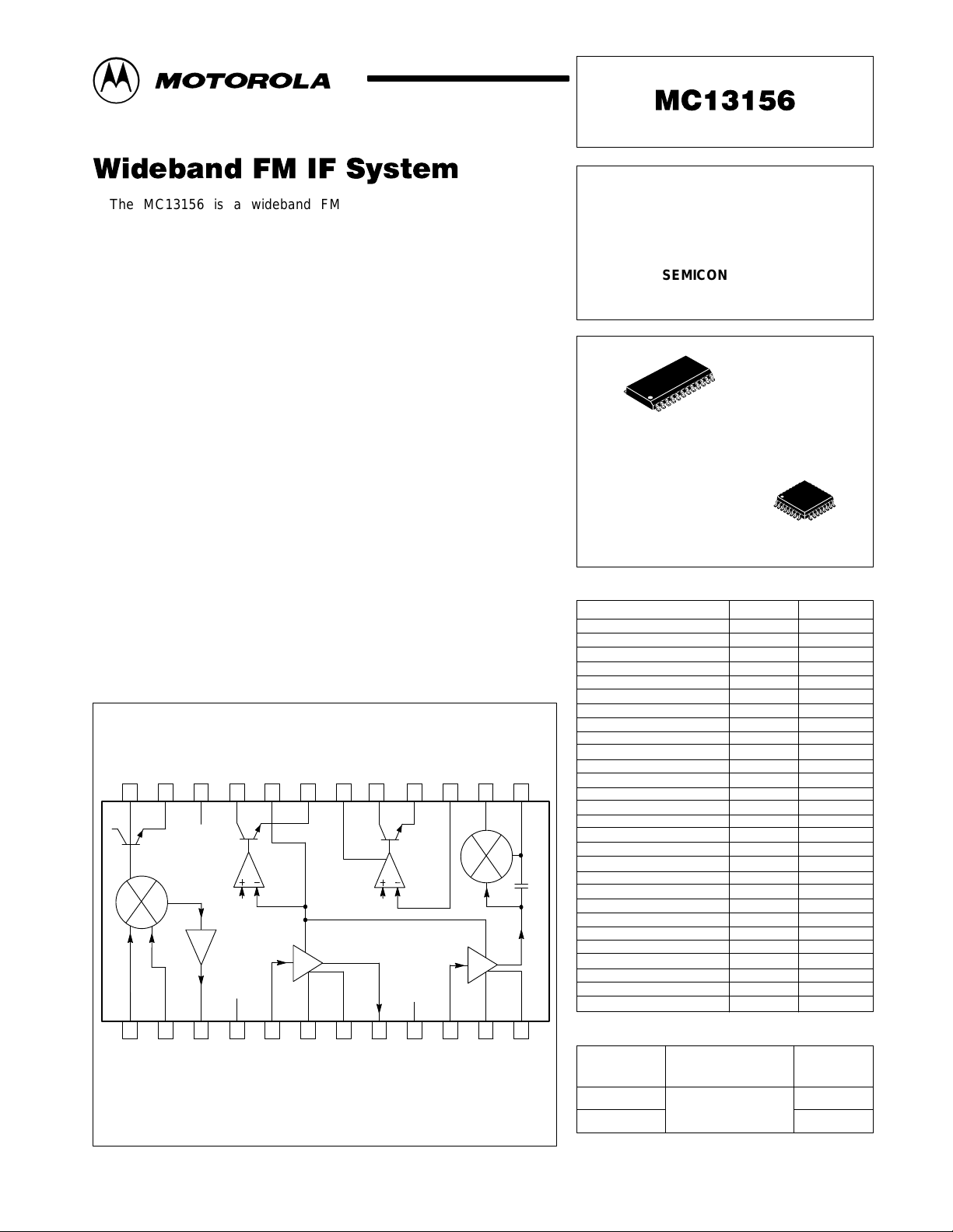
Simplified Block Diagram
DS
DS
Data
V
EE1
Mix
Out
CAR
Det
V
CC1
Bias
RSSI
IF
In
LO
LO
Emit
In
Mixer
RF
RF
In 2
In 1
NOTE: Pin Numbers shown for SOIC package only. Refer to Pin Assignments Table.
This device contains 197 active transistors.
V
EE2
IF
DEC 1
DS
Hold
IF Amp
DEC 2
18192022 1314151617212324
IF
Data
Slicer
Out
Out
Bias
IF
Gnd
V
CC2
In
LIM Amp
LIM
In
Demod
11
LIM
DEC 1
Quad
Coil
1210987654321
LIM
DEC 2
5.0
pF
PIN CONNECTIONS
Function
RF Input 1
RF Input 2
Mixer Output
V
CC1
IF Amp Input
IF Amp Decoupling 1
IF Amp Decoupling 2
VCC Connect (N/C Internal)
IF Amp Output
V
CC2
Limiter IF Input
Limiter Decoupling 1
Limiter Decoupling 2
VCC Connect (N/C Internal)
Quad Coil
Demodulator Output
Data Slicer Input
VCC Connect (N/C Internal)
Data Slicer Ground
Data Slicer Output
Data Slicer Hold
V
EE2
RSSI Output/Carrier Detect In
Carrier Detect Output
V
and Substrate
EE1
LO Emitter
LO Base
VCC Connect (N/C Internal)
ORDERING INFORMATION
Device
MC13156DW
MC13156FB
Temperature Range
TA = –40 to +85°C
SO–24L QFP
Operating
1
2
3
4
5
6
7
–
8
9
10
11
12
–
13
14
15
–
16
17
18
19
20
21
22
23
24
–
31
32
1
2
3
4
5
6
7
8
9
10
11
12, 13, 14
15
16
17
18
19
20
21
22
23
24
25
26
27
28, 29, 30
Package
SO–24L
QFP
MOTOROLA RF/IF DEVICE DATA
Motorola, Inc. 1998 Rev 2.1
1
Page 2
MC13156
MAXIMUM RATINGS
Rating Pin Symbol Value Unit
Power Supply Voltage 16, 19, 22 V
Junction Temperature – T
Storage Temperature Range – T
NOTES: 1. Devices should not be operated at or outside these values. The “Recommended Operating
Conditions” table provides for actual device operation.
2.ESD data available upon request.
EE(max)
J(max)
stg
RECOMMENDED OPERATING CONDITIONS
Rating Pin Symbol Value Unit
Power Supply Voltage @ TA = 25°C 4, 9 V
–40°C ≤ TA ≤ +85°C 16, 19, 22 V
Input Frequency 1, 2 f
Ambient Temperature Range – T
Input Signal Level 1, 2 V
DC ELECTRICAL CHARACTERISTICS (T
Characteristic
Total Drain Current (See Figure 2) 19, 22 I
VEE = –2.0 Vdc – 4.8 –
VEE = –3.0 Vdc 3.0 5.0 8.0
VEE = –5.0 Vdc – 5.2 –
VEE = –6.0 Vdc – 5.4 –
Drain Current, I22 (See Figure 3) 22 I
VEE = –2.0 Vdc – 3.0 –
VEE = –3.0 Vdc – 3.1 –
VEE = –5.0 Vdc – 3.3 –
VEE = –6.0 Vdc – 3.4 –
Drain Current, I19 (See Figure 3) 19 I
VEE = –2.0 Vdc – 1.8 –
VEE = –3.0 Vdc – 1.9 –
VEE = –5.0 Vdc – 1.9 –
VEE = –6.0 Vdc – 2.0 –
DATA SLICER (Input Voltage Referenced to VEE = –3.0 Vdc, no input signal; See Figure 15.)
Input Threshold Voltage (High Vin) 15 V
Output Current (Low Vin) 17 I
Data Slicer Enabled (No Hold)
V15 > 1.1 Vdc
V18 = 0 Vdc
= 25°C, V
A
CC1
= V
–6.5 Vdc
150 °C
–65 to +150 °C
CC
EE
in
A
in
= 0, no input signal.)
CC2
Pin Symbol Min Typ Max Unit
Total
22
19
15
17
1.0 1.1 1.2 Vdc
– 1.7 – mA
0 (Ground) Vdc
–2.0 to –6.0
500 MHz
–40 to +85 °C
200 mVrms
mA
mA
mA
AC ELECTRICAL CHARACTERISTICS (T
circuit, unless otherwise specified.)
Characteristic
12 dB SINAD Sensitivity (See Figures 17, 23) 1, 14 – – –100 – dBm
fin = 144.45 MHz; f
MIXER
Conversion Gain 1, 3 – – 22 – dB
Pin = –37 dBm (Figure 4)
Mixer Input Impedance 1, 2 R
Single–Ended (T able 1) C
Mixer Output Impedance 3 – – 330 – Ω
IF AMPLIFIER SECTION
IF RSSI Slope (Figure 6) 20 – 0.2 0.4 0.6 µA/dB
IF Gain (Figure 5) 5, 8 – – 39 – dB
Input Impedance 5 – – 1.4 – kΩ
Output Impedance 8 – – 290 – Ω
= 1.0 kHz; f
mod
dev
2
= 25°C, VEE = –3.0 Vdc, fRF = 130 MHz, fLO = 140.7 MHz, Figure 1 test
A
Pin Symbol Min Typ Max Unit
= ±75 kHz
p
p
– 1.0 – kΩ
– 4.0 – pF
MOTOROLA RF/IF DEVICE DATA
Page 3
MC13156
AC ELECTRICAL CHARACTERISTICS (continued) (T
circuit, unless otherwise specified.)
Characteristic UnitMaxTypMinSymbolPin
LIMITING AMPLIFIER SECTION
Limiter RSSI Slope (Figure 7) 20 – 0.2 0.4 0.6 µA/dB
Limiter Gain – – – 55 – dB
Input Impedance 10 – – 1.4 – kΩ
CARRIER DETECT
Output Current – Carrier Detect (High Vin) 21 – – 0 – µA
Output Current – Carrier Detect (Low Vin) 21 – – 3.0 – mA
Input Threshold Voltage – Carrier Detect 20 – 0.9 1.2 1.4 Vdc
Input Voltage Referenced to VEE = –3.0 Vdc
= 25°C, VEE = –3.0 Vdc, fRF = 130 MHz, fLO = 140.7 MHz, Figure 1 test
A
RF Input
130MHz
Mixer
Output
IF Input
IF Output
Limiter
Input
SMA
(1)
1:4
TR 1
330
50
1.0 n
330
50
1.0 n
200
1.0 n
1.0 n
1.0 n
10
11
1.0 n
12
1
2
3
4
5
6
7
8
9
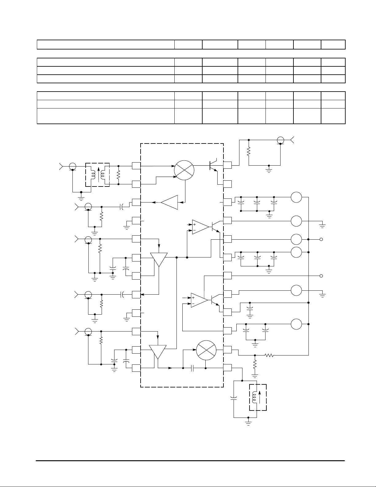
Figure 1. T est Circuit
MC13156
Mixer
V
CC
V
CC
LIM Amp
Bias
IF Amp
Bias
Data
Slicer
5.0 p
Local
Oscillator
1.0
1.0
µ
µ
Input
140.7MHz
200m Vrms
A
A
A
A
A
V
Carrier
Detect
V
EE
Data Slicer
Hold
50
24
23
22
V
EE
V
V
EE
EE
21
20
19
18
17
16
15
14
13
100 n
RSSI
Output
100 n
Data Output
1.0 n
1.0 n
1.0 n
100 k
100 k
+
+
1.0 n100 n
NOTES: 1. TR 1 Coilcraft 1:4 impedance transformer.
2.VCC is DC Ground.
3.1.5 µH variable shielded inductor:
T oko Part # 292SNS–T1373 or Equivalent.
MOTOROLA RF/IF DEVICE DATA
150 p
(3)
1.0 µH
3
Page 4

MC13156
DOCUMENT CONTAINS SCANNED IMAGES WHICH
COULD NOT BE PROCESSED FOR PDF FILES. FOR
COMPLETE DOCUMENT WITH IMAGES PLEASE
ORDER FROM MFAX OR THE LITERATURE
DISTRIBUTION CENTER
4
MOTOROLA RF/IF DEVICE DATA
Page 5
Figure 2. Total Drain Current versus Supply
V oltage and Temperature
6.5
(mA)
6.0
TOTAL
I
5.5
5.0
4.5
4.0
TOTAL DRAIN CURRENT,
3.5
1.0
2.0 3.0 4.0 5.0 6.0 7.0
VEE, SUPPLY VOLTAGE (–Vdc)
Figure 4. Mixer Gain versus Input Signal Level
25.0
TA = 85°C
55°C
25°C
–10°C
–40°C
MC13156
Figure 3. Drain Currents versus Supply V oltage
4.0
TA = 25°C
3.6
3.2
2.8
2.4
DRAIN CURRENTS (mA)
22
I
,
2.0
19
I
1.6
1.0 2.0 3.0 4.0 5.0 6.0 7.0
VEE, SUPPLY VOLTAGE (–Vdc)
I
22
I
19
Figure 5. IF Amplifier Gain versus Input
Signal Level and Ambient T emperature
40
22.5
20.0
TA = 25°C
17.5
15.0
MIXER GAIN (dB)
12.5
10.0
–90
–80 –70 –60 –50 –40 –30 –20 –10
Pin, RF INPUT SIGNAL LEVEL (dBm)
Figure 6. IF Amplifier RSSI Output Current versus
Input Signal Level and Ambient T emperature
µ
IF AMPLIFIER RSSI CURRENT ( A)
20.0
17.5
15.0
12.5
10.0
7.5
5.0
2.5
–50
0
VEE = –5.0 Vdc
f = 10.7 MHz
–40 –30 –20 –10 0 10
Pin, IF INPUT SIGNAL LEVEL (dBm)
TA = 25° to 85°C
–10°C
–40°C
38
36
34
32
30
IF AMPLIFIER GAIN (dB)
VEE = –5.0 Vdc
28
f = 10.7 MHz
26
–65
–60 –55 –50 –45 –40 –35 –30
Pin, IF INPUT SIGNAL LEVEL (dBm)
Figure 7. Limiter Amplifier RSSI Output Current
versus Input Signal Level and T emperature
µ
30
VEE = – 5.0 Vdc
f = 10.7 MHz
25
20
15
10
5.0
0
–70
LIMITER AMPLIFIER RSSI OUTPUT CURRENT ( A)
–60 –50 –40 –30 –20 –10 0 10
Pin, INPUT SIGNAL LEVEL (dBm)
TA = 25° to 85°C
85°C
55°C
25°C
–10°C
–40°C
–10°C
–40°C
MOTOROLA RF/IF DEVICE DATA
5
Page 6
MC13156
32 k
32 k
290
Detect
Carrier
out
IF
8
Figure 8.
Output
21
RSSI
Out
20
µ
400
µ
28
Demod
14
17
DS
Output
in
DS
15
Gnd
DS
16
DSHold
18
64 k64 k
64 k
Data Slicer
16 k
1.4 k
5
7
6
dec1
IF
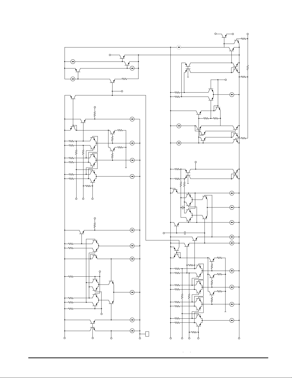
Figure 8. MC13156DW Internal Circuit Schematic
1.0 k 1.0 k
dec2
IF
in
IF
Mix
330
Output
3
in2
RF
in1
RF
2
1
13
coil
Quad
5.0 p
Linear Amplifier Quadrature Detector
4
CC1
V
Local Oscillator Mixer IF Amplifier RSSI Carrier Detect
base
O
24
23
emitter
EE1
V
22
6
CC2
V
9
11
dec1IMdec2
IM
12
10
in
LIM
EE2
V
19
MOTOROLA RF/IF DEVICE DATA
Page 7

MC13156
CIRCUIT DESCRIPTION
General
The MC13156 is a low power single conversion wideband
FM receiver incorporating a split IF . This device is designated
for use as the backend in digital FM systems such as CT–2
and wideband data links with data rates up to 500 kbaud. It
contains a mixer, oscillator, signal strength meter drive, IF
amplifier, limiting IF, quadrature detector and a data slicer
with a hold function (refer to Figure 8, Simplified Internal
Circuit Schematic).
Current Regulation
Temperature compensating voltage independent current
regulators are used throughout.
Mixer
The mixer is a double–balanced four quadrant multiplier
and is designed to work up to 500 MHz. It can be used in
differential or in single–ended mode by connecting the other
input to the positive supply rail.
Figure 4 shows the mixer gain and saturated output
response as a function of input signal drive. The circuit used
to measure this is shown in Figure 1. The linear gain of the
mixer is approximately 22 dB. Figure 9 shows the mixer gain
versus the IF output frequency with the local oscillator of
150 MHz at 100 mVrms LO drive level. The RF frequency is
swept. The sensitivity of the IF output of the mixer is shown in
Figure 10 for an RF input drive of 10 mVrms at 140 MHz and
IF at 10 MHz.
The single–ended parallel equivalent input impedance of
the mixer is Rp ~ 1.0 kΩ and Cp ~ 4.0 pF (see Table 1 for
details). The buffered output of the mixer is internally loaded
resulting in an output impedance of 330 Ω.
Local Oscillator
The on–chip transistor operates with crystal and LC
resonant elements up to 220 MHz. Series resonant, overtone
crystals are used to achieve excellent local oscillator stability .
3rd overtone crystals are used through about 65 to 70 MHz.
Operation from 70 MHz up to 180 MHz is feasible using the
on–chip transistor with a 5th or 7th overtone crystal. To
enhance operation using an overtone crystal, the internal
transistor’s bias is increased by adding an external resistor
from Pin 23 to VEE. –10 dBm of local oscillator drive is
needed to adequately drive the mixer (Figure 10).
The oscillator configurations specified above, and two
others using an external transistor, are described in the
application section:
1) A 133 MHz oscillator multiplier using a 3rd overtone
1) crystal, and
2) A 307.8 to 309.3 MHz manually tuned, varactor controlled
2) local oscillator.
RSSI
The Received Signal Strength Indicator (RSSI) output is a
current proportional to the log of the received signal
amplitude. The RSSI current output is derived by summing
the currents from the IF and limiting amplifier stages. An
external resistor at Pin 20 sets the voltage range or swing of
the RSSI output voltage. Linearity of the RSSI is optimized by
using external ceramic or crystal bandpass filters which have
an insertion loss of 8.0 dB. The RSSI circuit is designed to
provide 70+ dB of dynamic range with temperature
compensation (see Figures 6 and 7 which show RSSI
responses of the IF and Limiter amplifiers). Variation in the
RSSI output current with supply voltage is small (see
Figure 1 1).
Carrier Detect
When the meter current flowing through the meter load
resistance reaches 1.2 Vdc above ground, the comparator
flips, causing the carrier detect output to go high. Hysteresis
can be accomplished by adding a very large resistor for
positive feedback between the output and the input of the
comparator.
IF Amplifier
The first IF amplifier section is composed of three
differential stages with the second and third stages
contributing to the RSSI. This section has internal dc
feedback and external input decoupling for improved
symmetry and stability. The total gain of the IF amplifier block
is approximately 39 dB at 10.7 MHz. Figure 5 shows the gain
and saturated output response of the IF amplifier over
temperature, while Figure 12 shows the IF amplifier gain as a
function of the IF frequency.
The fixed internal input impedance is 1.4 kΩ. It is designed
for applications where a 455 kHz ceramic filter is used and no
external output matching is necessary since the filter requires
a 1.4 kΩ source and load impedance.
For 10.7 MHz ceramic filter applications, an external
430 Ω resistor must be added in parallel to provide the
equivalent load impedance of 330 Ω that is required by the
filter; however, no external matching is necessary at the input
since the mixer output matches the 330 Ω source impedance
of the filter. For 455 kHz applications, an external 1.1 kΩ
resistor must be added in series with the mixer output to
obtain the required matching impedance of 1.4 kΩ of the filter
input resistance. Overall RSSI linearity is dependent on
having total midband attenuation of 12 dB (6.0 dB insertion
loss plus 6.0 dB impedance matching loss) for the filter. The
output of the IF amplifier is buffered and the impedance is
290 Ω.
Limiter
The limiter section is similar to the IF amplifier section
except that four stages are used with the last three
contributing to the RSSI. The fixed internal input impedance
is 1.4 kΩ. The total gain of the limiting amplifier section is
approximately 55 dB. This IF limiting amplifier section
internally drives the quadrature detector section.
MOTOROLA RF/IF DEVICE DATA
7
Page 8

Figure 9. Mixer Gain versus IF Frequency
20
15
VEE = –3.0 Vdc
Vin = 1.0 mVrms (–47 dBm)
10
RO = 330
Rin = 50
BW(3.0 dB) = 21.7 MHz
5.0
fIF = fLO – f
–5.0
0
0.1
fLO = 150 MHz
VLO = 100 mVrms
MIXER GAIN (dB)
Figure 11. RSSI Output Current versus
Supply V oltage and RF Input Signal Level
40
Vin =
35
µ
–20 dBm
30
–40 dBm
25
–60 dBm
20
15
–80 dBm
10
RSSI OUTPUT CURRENT ( A)
–100 dBm
,
5.0
20
I
0
1.0
2.0 3.0 4.0 5.0 6.0 7.0
Ω
Ω
RF
1.0 10 100
fIF, IF FREQUENCY (MHz)
VEE, SUPPLY VOLTAGE (–Vdc)
TA = 25°C
MC13156
Figure 10. Mixer IF Output Level versus
Local Oscillator Input Level
–5.0
–10
–15
–20
–25
–30
–35
MIXER IF OUTPUT LEVEL (dBm)
–40
–45
–50 –40 –30 –20 –10 0 10
VEE = –3.0 Vdc
°
C
TA = 25
fRF = 140 MHz; fLO = 150 MHz
RF Input Level = –27 dBm
(10 mVrms)
Ω
Rin = 50
LO DRIVE (dBm)
; RO = 330
Ω
Figure 12. IF Amplifier Gain versus IF Frequency
60
50
40
30
Vin = 100 µV
Ω
20
IF AMPLIFIER GAIN (dB)
10
0
0.1
Rin = 50
RO = 330
BW(3.0 dB) = 26.8 MHz
TA = 25
1.0 10 100
f, FREQUENCY (MHz)
Ω
°
C
Figure 13. Recovered Audio Output Voltage
versus Supply V oltage
400
300
200
f
= 1.0 kHz
mod
±
75 kHz
f
=
dev
100
RECOVERED AUDIO OUTPUT (mVrms)V
,
14
0
1.0
2.0 3.0 4.0 5.0 6.0 7.0
VEE, SUPPLY VOLTAGE (–Vdc)
8
fRF = 140 MHz
RF Input Level = 1.0 mVrms
°
C
TA = 25
MOTOROLA RF/IF DEVICE DATA
Page 9

MC13156
Quadrature Detector
The quadrature detector is a doubly balanced four
quadrant multiplier with an internal 5.0 pF quadrature
capacitor to couple the IF signal to the external parallel RLC
resonant circuit that provides the 90 degree phase shift and
drives the quadrature detector. A single pin (Pin 13) provides
for the external LC parallel resonant network and the internal
connection to the quadrature detector.
The bandwidth of the detector allows for recovery of
relatively high data rate modulation. The recovered signal is
converted from differential to single ended through a
push–pull NPN/PNP output stage. Variation in recovered
audio output voltage with supply voltage is very small (see
Figure 13). The output drive capability is approximately
±9.0 µA for a frequency deviation of ±75 kHz and 1.0 kHz
modulating frequency (see Application Circuit).
Data Slicer
The data slicer input (Pin 15) is self centering around 1.1 V
with clamping occurring at 1.1 ± 0.5 Vbe Vdc. It is designed to
square up the data signal. Figure 14 shows a detailed
schematic of the data slicer.
The Voltage Regulator
Q12,
the Differential Input Amplifier. There is a potential of
1.0 Vbe on the base–collector of transistor diode Q11 and
2.0 Vbe on the base–collector of Q10. This sets up a 1.5 V
(~ 1.1 Vdc) on the node between the 36 kΩ resistors which is
connected to the base of Q12. The differential output of the
data slicer Q12 and Q13 is converted to a single–ended
output by the Driver Circuit. Additional circuitry, not shown in
Figure 14, tends to keep the data slicer input centered at
1.1 Vdc as input signal levels vary.
The Input Diode Clamp Circuit provides the clamping at
1.0 Vbe (0.75 Vdc) and 2.0 Vbe (1.45 Vdc). Transistor diodes
Q7 and Q8 are on, thus, providing a 2.0 Vbe potential at the
base of Q1. Also, the voltage regulator circuit provides a
potential of 2.0 Vbe on the base of Q3 and 1.0 Vbe on the
emitter of Q3 and Q2. When the data slicer input (Pin 15) is
sets up 1.1 Vdc on the base of
be
pulled up, Q1 turns off; Q2 turns on, thereby clamping the
input at 2.0 Vbe. On the other hand, when Pin 15 is pulled
down, Q1 turns on; Q2 turns off, thereby clamping the input at
1.0 Vbe.
The recovered data signal from the quadrature detector is
ac coupled to the data slicer via an input coupling capacitor.
The size of this capacitor and the nature of the data signal
determine how faithfully the data slicer shapes up the
recovered signal. The time constant is short for large peak to
peak voltage swings or when there is a change in dc level at
the detector output. For small signal or for continuous bits of
the same polarity which drift close to the threshold voltage,
the time constant is longer. When centered there is no input
current allowed, which is to say, that the input looks high in
impedance.
Another unique feature of the data slicer is that it responds
to various logic levels applied to the Data Slicer Hold Control
pin (Pin 18). Figure 15 illustrates how the input and output
currents under “no hold” condition relate to the input voltage.
Figure 16 shows how the input current and input voltage
relate for both the “no hold” and “hold” condition.
The hold control (Pin18) does three separate tasks:
1) With Pin 18 at 1.0 Vbe or greater, the output is shut off
(sets high). Q19 turns on which shunts the base drive
from Q20, thereby turning the output off.
2) With Pin 18 at 2.0 Vbe or greater, internal clamping diodes
are open circuited and the comparator input is shut off and
effectively open circuited. This is accomplished by turning
off the current source to emitters of the input differential
amplifier, thus, the input differential amplifier is shut off.
3) When the input is shut off, it allows the input capacitor to
hold its charge during transmit to improve recovery at the
beginning of the next receive period. When it is turned on,
it allows for very fast charging of the input capacitor for
quick recovery of new tuning or data average. The above
features are very desirable in a TDD digital FM system.
MOTOROLA RF/IF DEVICE DATA
9
Page 10

MC13156
Figure 14. Data Slicer Circuit
DS In
15
Q1
Q2
Q3
Q4
Q5
32 k
Q6
Q8
Q7
Q9
Q10
Q11
36 k
36 k
9
V
CC
Q12 Q13
8.0 k8.0 k
Q14
Q16
Q15
Q17
Data Out
17
Q20
16
DS Gnd
Q18
Q19
V
EE
19
Input Diode
Clamp Circuit
(Q1 to Q9)
16 k16 k
Voltage
Regulator
(Q10, Q11)
Figure 15. Data Slicer Input/Output Currents
versus Input V oltage
0.5
0.3
0.1
–0.1
INPUT CURRENT (mA)I
,
15
–0.3
–0.5
0.6
Output Current
(I17)
Input Current
(I15)
0.8 1.0 1.2
V15, INPUT VOLTAGE (Vdc)
VEE = –3.0 Vdc
V18 = 0 Vdc
(No Hold)
1.4 1.6 1.8
2.5
1.5
0.5
–0.5
–1.5
–2.5
OUTPUT CURRENT (mA)I
,
17
64 k
Differential
Input Amplifier
(Q12, Q13)
64 k
Driver and
Output Circuit
(Q14, Q20)
Figure 16. Data Slicer Input Current
versus Input V oltage
150
VEE = –3.0 Vdc
100
µ
50
0
INPUT CURRENT ( A)I
,
15
–50
–100
Hold
–1.0 –0.5 0 0.5 1.0 1.5 2.0
V15, INPUT VOLTAGE (Vdc)
No Hold
64 k
No Hold
V18 = 0 Vdc
18
DS Hold
Hold
V
≥ 1O
18
2.5 3.0
10
MOTOROLA RF/IF DEVICE DATA
Page 11

MC13156
Figure 17. MC13156DW Application Circuit
144.455 MHz
RF Input
V
CC
SMA
(2) 10.7 MHz
Ceramic
Filter
10 n
430
(2) 10.7 MHz
Ceramic
Filter
10 n
430
50 p7.5 p
(1)
0.1
µ
10 n
10 n
10 n
10
11
12
1
2
3
4
5
6
7
8
9
V
CC
V
CC
LIM Amp
Mixer
IF Amp
MC13156
Bias
Data
Slicer
Bias
5.0 p
(6)
0.146
µ
24
470
23
10 n
22
V
EE
21
20
47 k
19
V
EE
18
17
16
V
EE
100 n
15
180 p
14
13
+
1.0
MMBR5179
68 p
43 p
133.755 MHz
Osc/Tripler
100 k
10 n
10 n
10 k
100 k
100 k
µ
15 k
100 p
5.6 k
(5) 0.82
1.0 k
Carrier
Detect
RSSI
Output
Data Slicer
Hold
Data
Output
µ
(4) 3rd O.T.
XTAL
NOTES: 1. 0.1 µH V ariable Shielded Inductor: Coilcraft part # M1283–A or equivalent.
2.10.7 MHz Ceramic Filter: T oko part # SK107M5–A0–10X or Murata Erie part # SFE10.7MHY–A.
3.1.5 µH Variable Shielded Inductor: Toko part # 292SNS–T1373.
4.3rd Overtone, Series Resonant, 25 PPM Crystal at 44.585 MHz.
5.0.814 µH Variable Shielded Inductor: Coilcraft part # 143–18J12S.
6.0.146 µH Variable Inductor: Coilcraft part # 146–04J08.
MOTOROLA RF/IF DEVICE DATA
150 p
+
1.0
(3)
1.5
10 k
µ
µ
V
CC
11
Page 12

MC13156
APPLICATIONS INFORMATION
Component Selection
The evaluation PC board is designed to accommodate
specific components, while also being versatile enough to
use components from various manufacturers and coil types.
Figures NO TAG and NO TAG show the placement for the
components specified in the application circuit (Figure 17).
The applications circuit schematic specifies particular
components that were used to achieve the results shown in
the typical curves and tables but equivalent components
should give similar results.
Input Matching Networks/Components
The input matching circuit shown in the application circuit
schematic is passive high pass network which offers effective
image rejection when the local oscillator is below the RF input
frequency. Silver mica capacitors are used for their high Q
and tight tolerance. The PC board is not dedicated to any
particular input matching network topology; space is provided
for the designer to breadboard as desired.
Alternate matching networks using 4:1 surface mount
transformers or BALUN
S provide satisfactory performance.
The 12 dB SINAD sensitivity using the above matching
networks is typically –100 dBm for f
f
= ±75 kHz at fIN = 144.45 MHz and f
dev
= 1.0 kHz and
mod
= 133.75 MHz
OSC
(see Figure 23).
It is desirable to use a SAW filter before the mixer to
provide additional selectivity and adjacent channel rejection
and improved sensitivity. The SAW filter should be designed
to interface with the mixer input impedance of approximately
1.0 kΩ. Table 1 displays the series equivalent single–ended
mixer input impedance.
Local Oscillators
VHF Applications – The local oscillator circuit shown in the
application schematic utilizes a third overtone crystal and an
RF transistor. Selecting a transistor having good phase noise
performance is important; a mandatory criteria is for the
device to have good linearity of beta over several decades of
collector current. In other words, if the low current beta is
suppressed, it will not offer good 1/f noise performance. A
third overtone series resonant crystal having at least 25 ppm
tolerance over the operating temperature is recommended.
The local oscillator is an impedance inversion third overtone
Colpitts network and harmonic generator. In this circuit a 560
to 1.0 kΩ resistor shunts the crystal to ensure that it operates
in its overtone mode; thus, a blocking capacitor is needed to
eliminate the dc path to ground. The resulting parallel LC
network should “free–run” near the crystal frequency if a
short to ground is placed across the crystal. To provide
sufficient output loading at the collector, a high Q variable
inductor is used that is tuned to self resonate at the 3rd
harmonic of the overtone crystal frequency.
The on–chip grounded collector transistor may be used for
HF and VHF local oscillator with higher order overtone
crystals. Figure 18 shows a 5th overtone oscillator at
93.3 MHz and Figure 19 shows a 7th overtone oscillator at
148.3 MHz. Both circuits use a Butler overtone oscillator
configuration. The amplifier is an emitter follower . The crystal
is driven from the emitter and is coupled to the high
impedance base through a capacitive tap network. Operation
at the desired overtone frequency is ensured by the parallel
resonant circuit formed by the variable inductor and the tap
capacitors and parasitic capacitances of the on–chip
transistor and PC board. The variable inductor specified in
the schematic could be replaced with a high tolerance, high Q
ceramic or air wound surface mount component if the other
components have good tolerances. A variable inductor
provides an adjustment for gain and frequency of the
resonant tank ensuring lock up and startup of the crystal
oscillator. The overtone crystal is chosen with ESR of
typically 80 Ω and 120 Ω maximum; if the resistive loss in the
crystal is too high, the performance of the oscillator may be
impacted by lower gain margins.
12
T able 1. Mixer Input Impedance Data
(Single–ended configuration, VCC = 3.0 Vdc, local oscillator drive = 100 mVrms)
Series Equivalent
Frequency
(MHz)
90 190 – j380 950 4.7
100 160 – j360 970 4.4
110 130 – j340 1020 4.2
120 110 – j320 1040 4.2
130 97 – j300 1030 4.0
140 82 – j280 1040 4.0
150 71 – j270 1100 4.0
160 59 – j260 1200 3.9
170 52 – j240 1160 3.9
180 44 – j230 1250 3.8
190 38 – j220 1300 3.8
Complex Impedance
(R + jX)
(Ω)
Parallel
Resistance
Rp
(Ω)
Parallel
Capacitance
Cp
(pF)
MOTOROLA RF/IF DEVICE DATA
Page 13

MC13156
A series LC network to ground (which is VCC) is comprised
of the inductance of the base lead of the on–chip transistor
and PC board traces and tap capacitors. Parasitic
oscillations often occur in the 200 to 800 MHz range. A small
resistor is placed in series with the base (Pin 24) to cancel the
negative resistance associated with this undesired mode of
oscillation. Since the base input impedance is so large a
small resistor in the range of 27 to 68 Ω has very little effect
on the desired Butler mode of oscillation.
The crystal parallel capacitance, Co, provides a feedback
path that is low enough in reactance at frequencies of 5th
overtone or higher to cause trouble. Co has little effect near
resonance because of the low impedance of the crystal
motional arm (Rm–Lm–Cm). As the tunable inductor which
forms the resonant tank with the tap capacitors is tuned off
the crystal resonant frequency, it may be difficult to tell if the
oscillation is under crystal control. Frequency jumps may
occur as the inductor is tuned. In order to eliminate this
behavior an inductor (Lo) is placed in parallel with the crystal.
Lo is chosen to resonant with the crystal parallel capacitance
(Co) at the desired operation frequency. The inductor
provides a feedback path at frequencies well below
resonance; however, the parallel tank network of the tap
capacitors and tunable inductor prevent oscillation at these
frequencies.
UHF Application
Figure 20 shows a 318.5 to 320 MHz receiver which drives
the mixer with an external varactor controlled (307.8 to
309.3 MHz) LC oscillator using an MPS901 (RF low power
transistor in a TO–92 plastic package; also MMBR901 is
available in a SOT–23 surface mount package). With the
50 kΩ 10 turn potentiometer this oscillator is tunable over a
range of approximately 1.5 MHz. The MMBV909L is a low
voltage varactor suitable for UHF applications; it is a dual
back–to–back varactor in a SOT–23 package. The input
matching network uses a 1:4 impedance matching
transformer (Recommended sources are Mini–Circuits and
Coilcraft).
Using the same IF ceramic filters and quadrature detector
circuit as specified in the applications circuit in Figure 17, the
12 dB SINAD performance is –95 dBm for a f
sinusoidal waveform and f
±40 kHz.
dev
mod
= 1.0 kHz
This circuit is breadboarded using the evaluation PC board
shown in Figures NO TAG and NO TAG. The RF ground is
VCC and path lengths are minimized. High quality surface
mount components were used except where specified. The
absolute values of the components used will vary with layout
placement and component parasitics.
RSSI Response
Figure 24 shows the full RSSI response in the application
circuit. The 10.7 MHz, 1 10 kHz wide bandpass ceramic filters
(recommended sources are TOKO part # SK107M5–AO–10X
or Murata Erie SFE10.7MHY–A) provide the correct
bandpass insertion loss to linearize the curve between the
limiter and IF portions of RSSI. Figure 23 shows that limiting
occurs at an input of –100 dBm. As shown in Figure 24, the
RSSI output linear from –100 dBm to –30 dBm.
The RSSI rise and fall times for various RF input signal
levels and R20 values are measured at Pin 20 without 10 nF
filter capacitor. A 10 kHz square wave pulses the RF input
signal on and off. Figure 25 shows that the rise and fall times
are short enough to recover greater than 10 kHz ASK data;
with a wider IF bandpass filters data rates up to 50 kHz may
be achieved. The circuit used is the application circuit in
Figure 17 with no RSSI output filter capacitor.
104 MHz
RF Input
Figure 18. MC13156DW Application Circuit
fRF = 104 MHz; fLO = 93.30 MHz
5th Overtone Crystal Oscillator
(2)
10 p
SMA
3.0 p
NOTES: 1. 0.1 µH V ariable Shielded Inductor: Coilcraft part # M1283–A or equivalent.
2.Capacitors are Silver Mica.
3.5th Overtone, Series Resonant, 25 PPM Crystal at 93.300 MHz.
4.0.135 µH Variable Shielded Inductor: Coilcraft part # 146–05J08S or equivalent.
(1)
0.1
To Filter
120 p
1
µ
2
10 n
3
Mixer
V
EE
24
23
4.7 k
22
33
µ
1.0
(3)
5th OT
XTAL
(4)
µ
H
0.135
+
1.0
µ
27 p
H
30 p
10 n
V
CC
MOTOROLA RF/IF DEVICE DATA
13
Page 14

MC13156
Figure 19. MC13156DW Application Circuit
fRF = 159 MHz; fLO = 148.30 MHz
7th Overtone Crystal Oscillator
33
(4)
76 nH
+
1.0
µ
159 MHz
RF Input
SMA
(2)
5.0 p
50 p
1
Mixer
24
(1)
µ
H
0.08
470
2
10 n
3
23
4.7 k
22
V
EE
To IF Filter
NOTES: 1. 0.08 µH Variable Shielded Inductor: Toko part # 292SNS–T1365Z or equivalent.
2.Capacitors are Silver Mica.
3.7th Overtone, Series Resonant, 25 PPM Crystal at 148.300 MHz.
4.76 nH Variable Shielded Inductor: Coilcraft part # 150–03J08S or equivalent.
Figure 20. MC13156DW Varactor Controlled LC Oscillator
0.22
(3)
7th OT
XTAL
27 p
µ
H
47 p
10 n
V
CC
(2)
47 k
50 k
318.5 to
320 MHz
RF Input
SMA
(1)
1:4 Transformer
Mixer
1
2
3
NOTES: 1. 1:4 Impedance T ransformer: Mini–Circuits.
2.50 k Potentiometer, 10 turns.
3. Spring Coil; Coilcraft A05T .
4.Dual Varactor in SOT–23 Package.
5. All other components are surface mount components.
6.Ferrite beads through loop of 24 AWG wire.
1.0 M
V
VCO
0.1
(4)
µ
24
(6)
4.7 k
MPS901
20 p
+
6.8 p
24 p
1.0
µ
MMBV909L
23
22
V
EE
1.8 k
12 k
24 p
(3)
18.5 nH
1.0 n
307.8–309.3 MHz
LC Varactor
Controlled Oscillator
VCC = 3.3 Vdc (Reg)
14
MOTOROLA RF/IF DEVICE DATA
Page 15

MC13156
45 MHz Narrowband Receiver
The above application examples utilize a 10.7 MHz IF. In
this section a narrowband receiver with a 455 kHz IF will be
described. Figure 21 shows a full schematic of a 45 MHz
receiver that uses a 3rd overtone crystal with the on–chip
oscillator transistor. The oscillator configuration is similar to
the one used in Figure 17; it is called an impedance inversion
Colpitts. A 44.545 MHz 3rd overtone, series resonant crystal
is used to achieve an IF frequency at 455 kHz. The ceramic
IF filters selected are Murata Erie part # SFG455A3. 1.2 kΩ
chip resistors are used in series with the filters to achieve the
terminating resistance of 1.4 kΩ to the filter. The IF
decoupling is very important; 0.1 µF chip capacitors are used
at Pins 6, 7, 11 and 12. The quadrature detector tank circuit
uses a 455 kHz quadrature tank from Toko.
Figure 21. MC13156DW Application Circuit at 45 MHz
The 12 dB SINAD performance is –109 dBm for a f
1.0 kHz and a f
= ±4.0 kHz. The RSSI dynamic range is
dev
mod
approximately 80 dB of linear range (see Figure 22).
Receiver Design Considerations
The curves of signal levels at various portions of the
application receiver with respect to RF input level are shown
in Figure 26. This information helps determine the network
topology and gain blocks required ahead of the MC13156 to
achieve the desired sensitivity and dynamic range of the
receiver system. In the application circuit the input third order
intercept (IP3) performance of the system is approximately
–25 dBm (see Figure 27).
µ
H
1.8
(6)
+
1.0
µ
=
45 Hz
RF Input
SMA
V
CC
180 p
(2) 455 kHz
(2) 455 kHz
33 p
10 n
Ceramic
Filter
µ
0.1
Ceramic
Filter
0.1
µ
(1)
0.33
1.2 k
0.1
1.2 k
0.1
56 p
39 p
47 k
100 n
10 n
100 k
10 k
(5) 0.416
10 k
10 n
100 k
100 k
10 n
10 n
µ
H
470 k
Carrier
Detect
RSSI
Output
Data Slicer
Hold
Data
Output
Audio To
C–Message
Filter and
Amp.
(4) 3rd OT
XTAL
44.545
MHz
µ
H
1
2
3
4
5
6
µ
7
8
9
10
11
µ
12
V
V
CC
CC
Mixer
IF Amp
LIM Amp
Bias
Bias
Data
Slicer
5.0 p
24
23
22
V
EE
21
20
19
V
EE
18
17
16
V
EE
15
14
1.0 n
13
NOTES: 1. 0.33 µH Variable Shielded Inductor: Coilcraft part # 7M3–331 or equivalent.
2.455 kHz Ceramic Filter: Murata Erie part # SFG455A3.
3.455 kHz Quadrature Tank: Toko part # 7MC8128Z.
4.3rd Overtone, Series Resonant, 25 PPM Crystal at 44.540 MHz.
5. 0.416 µH Variable Shielded Inductor: Coilcraft part # 143–10J12S.
6. 1.8 µH Molded Inductor.
MOTOROLA RF/IF DEVICE DATA
(3)
180 p
27 k
+
1.0
µ
680 µH
VCC = 2.0 to 5.0 Vdc
15
Page 16

É
É
1.8
Ç
Ç
1.6
1.4
1.2
1.0
0.8
RSSI OUTPUT VOLTAGE (Vdc)
0.6
0.4
–120
Figure 22. RSSI Output Voltage
versus Input Signal Level
fRF = 45.00 MHz
VCC = 2.0 Vdc
12 dB SINAD @ –109 dBm
µ
Vrms)
(0.8
(See Figure 21)
–100 –80
–60 –40 20
SIGNAL INPUT LEVEL (dBm)
–20 0
MC13156
Figure 23. S + N/N versus RF Input Signal Level
10
0
–10
–20
S + N, N (dB)
–30
–40
–50
–110
–100
–90 –80 –70
RF INPUT SIGNAL (dBm)
S+N
VCC = 5.0 Vdc
f
dev
f
mod
fin = 144.45 MHz
(See Figure 17)
N
–60 –50 –40 –30 –20
±
75 kHz
=
= 1.0 kHz
Figure 24. RSSI Output Voltage
versus Input Signal Level
1.4
1.2
1.0
0.8
VCC = 5.0 Vdc
0.6
0.4
RSSI OUTPUT VOLTAGE (Vdc)
fc = 144.455 MHz
fLO = 133.755 MHz
Low Loss 10.7 MHz
Ceramic Filter
(See Figure 17)
0.2
–120 –100 –80 –60 –40 –20 0
SIGNAL INPUT LEVEL (dBm)
Figure 26. Signal Levels versus
RF Input Signal Level
0
LO Level = –2.0 dBm
–10
(See Figure 17)
–20
–30
–40
POWER (dBm)
–50
–60
–70
–100
–90 –80 –70 –60 –50 –40
IF Output
Limiter Input
–30
Figure 25. RSSI Output Rise and Fall Times
versus RF Input Signal Level
35
µ
30
25
20
15
10
RSSI RISE AND FALL TIMES ( s)t
5.0
rf
t , ,
0
0 –20
–40 –60 –80
RF INPUT SIGNAL LEVEL (dBm)
Figure 27. 1.0 dB Compression Pt. and Input
Third Order Intercept Pt. versus Input Power
10
VCC = 5.0 Vdc
–10
–20
–30
–40
–50
MIXER IF OUTPUT LEVEL (dBm)
–60
–70
0
f
= 144.4 MHz
RF1
f
= 144.5 MHz
RF2
fLO = 133.75 MHz
PLO = –2.0 dBm
(See Figure 17)
–100
–80 –60 –40
1.0 dB Comp. Pt.
= –37 dBm
RF INPUT POWER (dBm)RF INPUT SIGNAL LEVEL (dBm)
tr@ 22 k
tf @ 22 k
tr@ 47 k
tf @ 47 k
tr@ 100 k
tf@ 100 k
IP3 = –25 dBm
–20 0
16
MOTOROLA RF/IF DEVICE DATA
Page 17

MC13156
BER TESTING AND PERFORMANCE
Description
The test setup shown in Figure 29 is configured so that the
function generator supplies a 100 kHz clock source to the bit
error rate tester. This device generates and receives a
repeating data pattern and drives a 5 pole baseband data
filter. The filter effectively reduces harmonic content of the
baseband data which is used to modulate the RF generator
which is running at 144.45 MHz. Following processing of the
signal by the receiver (MC13156), the recovered baseband
sinewave (data) is AC coupled to the data slicer. The data
slicer is essentially an auto–threshold comparator which
tracks the zero crossing of the incoming sinewave and
provides logic level data at its ouput. Data errors associated
with the recovered data are collected by the bit error rate
receiver and displayed.
Bit error rate versus RF signal input level and IF filter
bandwidth are shown in Figure 28. The bit error rate data was
taken under the following test conditions:
• Data rate = 100 kbps
• Filter cutoff frequency set to 39% of the data rate or 39 kHz.
• Filter type is a 5 pole equal–ripple with 0.5° phase error.
• VCC = 4.0 Vdc
• Frequency deviation = ±32 kHz.
Figure 28. Bit Error Rate versus RF
Input Signal Level and IF Bandpass Filter
–1
10
VCC = 4.0 Vdc
Data Pattern = 2E09 Prbs NRZ
Baseband Filter fc = 50 kHz
±
32 kHz
f
=
dev
IF Filter BW
230 kHz
BER, BIT ERROR RA TE
10
10
10
–3
–5
–7
–90
IF Filter BW
110 kHz
–85 –80 –75 –70
RF INPUT SIGNAL LEVEL (dBm)
Evaluation PC Board
The evaluation PCB is very versatile and is intended to be
used across the entire useful frequency range of this device.
The center section of the board provides an area for
attaching all SMT components to the circuit side and radial
leaded components to the component ground side (see
Figures NO TAG and NO TAG). Additionally, the peripheral
area surrounding the RF core provides pads to add
supporting and interface circuitry as a particular application
dictates.
MOTOROLA RF/IF DEVICE DATA
17
Page 18

MC13156
Figure 29. Bit Error Rate Test Setup
Function Generator
Wavetek Model No. 164 HP3780A or Equivalent HP8640B
Gen
Clock
Out
Clock
Input
Bit Error Rate Tester RF Generator
Rcr
Clock
Input
Rcr
Data
Input
Generator
Input
Modulation
Input
5 Pole
Bandpass
Filter
Data Slicer
Output
Mixer
Input
MC13156
UUT
RF
Output
18
MOTOROLA RF/IF DEVICE DATA
Page 19

MC13156
OUTLINE DIMENSIONS
FB SUFFIX
PLASTIC QFP PACKAGE
CASE 873–01
L
ISSUE A
24
25
–A–
L
17
16
–B–
S
S
A–B
C
M
B
S
S
A–B
H
A–B0.05 (0.002)
V
M
B
0.20 (0.008) D
DETAIL A
32
18
9
0.20 (0.008) D
B
P
–A–, –B–, –D–
–D–
DETAIL A
A
0.20 (0.008) D
M
S
A–B
C
S
A–B0.05 (0.002)
S
0.20 (0.008) D
M
S
A–B
H
S
M
DETAIL C
BASE
METAL
J
F
N
–C–
SEATING
PLANE
–H–
DATUM
PLANE
E
C
H
G
M
–H–
DATUM
PLANE
0.01 (0.004)
D
0.20 (0.008) D
M
S
A–B
C
S
SECTION B–B
DETAIL C
VIEW ROTATED 90 CLOCKWISE
U
T
R
K
Q
X
NOTES:
1. DIMENSIONING AND TOLERANCING PER ANSI
Y14.5M, 1982.
2. CONTROLLING DIMENSION: MILLIMETER.
3. DATUM PLANE –H– IS LOCATED AT BOTTOM OF
LEAD AND IS COINCIDENT WITH THE LEAD WHERE
THE LEAD EXITS THE PLASTIC BODY AT THE
BOTTOM OF THE PARTING LINE.
4. DATUMS –A–, –B– AND –D– TO BE DETERMINED AT
DATUM PLANE –H–.
5. DIMENSIONS S AND V TO BE DETERMINED AT
SEATING PLANE –C–.
6. DIMENSIONS A AND B DO NOT INCLUDE MOLD
PROTRUSION. ALLOWABLE PROTRUSION IS 0.25
(0.010) PER SIDE. DIMENSIONS A AND B DO
INCLUDE MOLD MISMATCH AND ARE DETERMINED
AT DATUM PLANE –H–.
7. DIMENSION D DOES NOT INCLUDE DAMBAR
PROTRUSION. ALLOWABLE DAMBAR PROTRUSION
SHALL BE 0.08 (0.003) TOTAL IN EXCESS OF THE D
DIMENSION AT MAXIMUM MATERIAL CONDITION.
DAMBAR CANNOT BE LOCATED ON THE LOWER
RADIUS OR THE FOOT.
DIM MIN MAX MIN MAX
A 6.95 0.274 0.280
B 6.95 7.10 0.274 0.280
C 1.40 1.60 0.055 0.063
D 0.273 0.373 0.010 0.015
E 1.30 1.50 0.051 0.059
F 0.273 ––– 0.010 –––
G 0.80 BSC 0.031 BSC
H ––– 0.20 ––– 0.008
J 0.119 0.197 0.005 0.008
K 0.33 0.57 0.013 0.022
L 5.6 REF 0.220 REF
M 6 8 6 8
N 0.119 0.135 0.005 0.005
P 0.40 BSC 0.016 BSC
Q 5 10 5 10
R 0.15 0.25 0.006 0.010
S 8.85 9.15 0.348 0.360
T 0.15 0.25 0.006 0.010
U 5 11 5 11
V 8.85 9.15 0.348 0.360
X 1.00 REF 0.039 REF
_
INCHESMILLIMETERS
7.10
____
__ __
__ __
MOTOROLA RF/IF DEVICE DATA
19
Page 20

–T–
SEATING
PLANE
MC13156
OUTLINE DIMENSIONS
DW SUFFIX
PLASTIC PACKAGE
CASE 751E–04
(SO–24L)
ISSUE E
–A–
1324
–B– P12X
M
0.010 (0.25) B
1
D24X
0.010 (0.25) B
M
T
12
J
S
A
S
M
F
R
C
M
22X
G
K
NOTES:
1. DIMENSIONING AND TOLERANCING PER ANSI
Y14.5M, 1982.
2. CONTROLLING DIMENSION: MILLIMETER.
3. DIMENSIONS A AND B DO NOT INCLUDE
MOLD PROTRUSION.
4. MAXIMUM MOLD PROTRUSION 0.15 (0.006)
PER SIDE.
5. DIMENSION D DOES NOT INCLUDE DAMBAR
PROTRUSION. ALLOWABLE DAMBAR
PROTRUSION SHALL BE 0.13 (0.005) TOTAL IN
EXCESS OF D DIMENSION AT MAXIMUM
MATERIAL CONDITION.
DIM MIN MAX MIN MAX
A 15.25 15.54 0.601 0.612
B 7.40 7.60 0.292 0.299
C 2.35 2.65 0.093 0.104
X 45
D 0.35 0.49 0.014 0.019
_
F 0.41 0.90 0.016 0.035
G 1.27 BSC 0.050 BSC
J 0.23 0.32 0.009 0.013
K 0.13 0.29 0.005 0.01 1
M 0 8 0 8
P 10.05 10.55 0.395 0.415
R 0.25 0.75 0.010 0.029
INCHESMILLIMETERS
____
Motorola reserves the right to make changes without further notice to any products herein. Motorola makes no warranty , representation or guarantee regarding
the suitability of its products for any particular purpose, nor does Motorola assume any liability arising out of the application or use of any product or circuit, and
specifically disclaims any and all liability, including without limitation consequential or incidental damages. “T ypical” parameters which may be provided in Motorola
data sheets and/or specifications can and do vary in different applications and actual performance may vary over time. All operating parameters, including “Typicals”
must be validated for each customer application by customer’s technical experts. Motorola does not convey any license under its patent rights nor the rights of
others. Motorola products are not designed, intended, or authorized for use as components in systems intended for surgical implant into the body, or other
applications intended to support or sustain life, or for any other application in which the failure of the Motorola product could create a situation where personal injury
or death may occur. Should Buyer purchase or use Motorola products for any such unintended or unauthorized application, Buyer shall indemnify and hold Motorola
and its officers, employees, subsidiaries, affiliates, and distributors harmless against all claims, costs, damages, and expenses, and reasonable attorney fees
arising out of, directly or indirectly, any claim of personal injury or death associated with such unintended or unauthorized use, even if such claim alleges that
Motorola was negligent regarding the design or manufacture of the part. Motorola and are registered trademarks of Motorola, Inc. Motorola, Inc. is an Equal
Opportunity/Affirmative Action Employer.
How to reach us:
USA/EUROPE/ Locations Not Listed: Motorola Literature Distribution; JAPAN: Nippon Motorola Ltd.: SPD, Strategic Planning Office, 141,
P.O. Box 5405, Denver, Colorado 80217. 1–303–675–2140 or 1–800–441–2447 4–32–1 Nishi–Gotanda, Shagawa–ku, Tokyo, Japan. 03–5487–8488
Customer Focus Center: 1–800–521–6274
Mfax: RMFAX0@email.sps.mot.com – TOUCHT ONE 1–602–244–6609 ASIA/PACIFIC: Motorola Semiconductors H.K. Ltd.; 8B Tai Ping Industrial Park,
Moto rola Fax Back Sys tem – US & Canada ONLY 1–800–774–1848 51 Ting Kok Road, Tai Po, N.T., Hong Kong. 852–26629298
HOME PAGE: http://motorola.com/sps/
20
– http://sps.motorola.com/mfax/
◊
Mfax is a trademark of Motorola, Inc.
MOTOROLA RF/IF DEVICE DATA
MC13156/D
 Loading...